ICGOO在线商城 > SN74LV32ADBR

 Datasheet下载
- 型号: SN74LV32ADBR
- 制造商: Texas Instruments
- 库位|库存: xxxx|xxxx
- 要求:
| 数量阶梯 | 香港交货 | 国内含税 |
| +xxxx | $xxxx | ¥xxxx |
查看当月历史价格
查看今年历史价格
SN74LV32ADBR产品简介:
ICGOO电子元器件商城为您提供SN74LV32ADBR由Texas Instruments设计生产,在icgoo商城现货销售,并且可以通过原厂、代理商等渠道进行代购。 提供SN74LV32ADBR价格参考以及Texas InstrumentsSN74LV32ADBR封装/规格参数等产品信息。 你可以下载SN74LV32ADBR参考资料、Datasheet数据手册功能说明书, 资料中有SN74LV32ADBR详细功能的应用电路图电压和使用方法及教程。
| 参数 | 数值 |
| 产品目录 | 集成电路 (IC)半导体 |
| 描述 | IC GATE OR 4CH 2-INP 14-SSOP逻辑门 Quad 2-Input Pos |
| 产品分类 | |
| 品牌 | Texas Instruments |
| 产品手册 | |
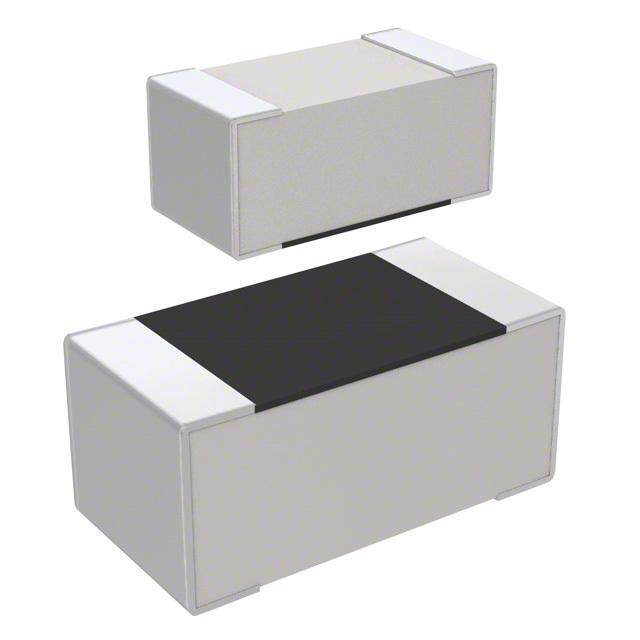
| 产品图片 |
|
| rohs | 符合RoHS无铅 / 符合限制有害物质指令(RoHS)规范要求 |
| 产品系列 | 逻辑集成电路,逻辑门,Texas Instruments SN74LV32ADBR74LV |
| 数据手册 | |
| 产品型号 | SN74LV32ADBR |
| 不同V、最大CL时的最大传播延迟 | 7.5ns @ 5V,50pF |
| 产品 | OR |
| 产品目录页面 | |
| 产品种类 | 逻辑门 |
| 传播延迟时间 | 13 ns |
| 低电平输出电流 | 12 mA |
| 供应商器件封装 | 14-SSOP |
| 其它名称 | 296-3817-1 |
| 包装 | 剪切带 (CT) |
| 单位重量 | 121.800 mg |
| 商标 | Texas Instruments |
| 安装类型 | 表面贴装 |
| 安装风格 | SMD/SMT |
| 封装 | Reel |
| 封装/外壳 | 14-SSOP(0.209",5.30mm 宽) |
| 封装/箱体 | SSOP-14 |
| 工作温度 | -40°C ~ 85°C |
| 工作温度范围 | - 40 C to + 85 C |
| 工厂包装数量 | 2000 |
| 最大工作温度 | + 85 C |
| 最小工作温度 | - 40 C |
| 栅极数量 | 4 Gate |
| 标准包装 | 1 |
| 特性 | - |
| 电压-电源 | 2 V ~ 5.5 V |
| 电流-输出高,低 | 12mA,12mA |
| 电流-静态(最大值) | 20µA |
| 电源电压-最大 | 5.5 V |
| 电源电压-最小 | 2 V |
| 电路数 | 4 |
| 系列 | SN74LV32A |
| 输入/输出线数量 | 2 / 1 |
| 输入数 | 2 |
| 输入线路数量 | 2 |
| 输出线路数量 | 1 |
| 逻辑电平-低 | 0.5V |
| 逻辑电平-高 | 1.5V |
| 逻辑类型 | 或门 |
| 逻辑系列 | LV-A |
| 高电平输出电流 | - 12 mA |


PDF Datasheet 数据手册内容提取
Product Sample & Technical Tools & Support & Folder Buy Documents Software Community SN74LV32A SCLS385K–SEPTEMBER1997–REVISEDDECEMBER2014 SN74LV32A Quadruple 2-Input Positive-Or Gates 1 Features 2 Applications • 2-Vto5.5-VV Operation • Printers 1 CC • Maxt of6.5nsat5V • E-Meters pd • TypicalV (OutputGroundBounce) • MotorControls:PermanentMagnets OLP <0.8VatVCC=3.3V,TA=25°C • ServersandHighPerformanceComputing • TypicalVOHV(OutputVOH Undershoot) • AutomotiveInfotainment >2.3VatV =3.3V,T =25°C CC A • SupportMixed-ModeVoltageOperationon 3 Description AllPorts This quadruple 2-input positive-OR gates is designed • IoffSupportsPartial-Power-DownModeOperation for2-Vto5.5-VVCCoperation. • Latch-UpPerformanceExceeds250mAPer The SN74LV32A device performs the Boolean JESD17 functionY(cid:2)A(cid:1)BorY(cid:2)A•Binpositivelogic. • ESDProtectionExceedsJESD22 DeviceInformation(1) – 2000-VHuman-BodyModel PARTNUMBER PACKAGE BODYSIZE(NOM) – 200-VMachineModel TVSOP(14) 3.60mmx4.40mm – 1000-VCharged-DeviceModel SOIC(14) 8.65mm×3.91mm SN74LV32A VQFN(14) 3.50mmx3.50mm SSOP(14) 6.20mmx5.30mm TSSOP(14) 5.00mmx4.40mm (1) For all available packages, see the orderable addendum at theendofthedatasheet. 4 Simplified Schematic A Y B 1 An IMPORTANT NOTICE at the end of this data sheet addresses availability, warranty, changes, use in safety-critical applications, intellectualpropertymattersandotherimportantdisclaimers.PRODUCTIONDATA.
SN74LV32A SCLS385K–SEPTEMBER1997–REVISEDDECEMBER2014 www.ti.com Table of Contents 1 Features.................................................................. 1 9 DetailedDescription.............................................. 9 2 Applications........................................................... 1 9.1 Overview...................................................................9 3 Description............................................................. 1 9.2 FunctionalBlockDiagram.........................................9 4 SimplifiedSchematic............................................. 1 9.3 FeatureDescription...................................................9 9.4 DeviceFunctionalModes..........................................9 5 RevisionHistory..................................................... 2 10 ApplicationandImplementation........................ 10 6 PinConfigurationandFunctions......................... 3 10.1 ApplicationInformation..........................................10 7 Specifications......................................................... 4 10.2 TypicalApplication ...............................................10 7.1 AbsoluteMaximumRatings......................................4 11 PowerSupplyRecommendations..................... 11 7.2 ESDRatings..............................................................4 12 Layout................................................................... 12 7.3 RecommendedOperatingConditions.......................5 7.4 ThermalInformation..................................................5 12.1 LayoutGuidelines.................................................12 7.5 ElectricalCharacteristics...........................................6 12.2 LayoutExample....................................................12 7.6 SwitchingCharacteristics,V =2.5V±0.2V........6 13 DeviceandDocumentationSupport................. 12 CC 7.7 SwitchingCharacteristics,V =3.3V±0.3V........6 13.1 RelatedLinks........................................................12 CC 7.8 SwitchingCharacteristics,V =5V±0.5V...........6 13.2 Trademarks...........................................................12 CC 7.9 NoiseCharacteristics................................................7 13.3 ElectrostaticDischargeCaution............................12 7.10 OperatingCharacteristics........................................7 13.4 Glossary................................................................12 7.11 TypicalCharacteristics............................................7 14 Mechanical,Packaging,andOrderable Information........................................................... 12 8 ParameterMeasurementInformation..................8 5 Revision History ChangesfromRevisionJ(April2005)toRevisionK Page • AddedApplications,DeviceInformationtable,PinFunctionstable,ESDRatingstable,ThermalInformationtable, TypicalCharacteristics,FeatureDescriptionsection,DeviceFunctionalModes,ApplicationandImplementation section,PowerSupplyRecommendationssection,Layoutsection,DeviceandDocumentationSupportsection,and Mechanical,Packaging,andOrderableInformationsection.................................................................................................. 1 • DeletedOrderingInformationtable........................................................................................................................................ 1 • ChangedMAXoperatingtemperatureto125°CinRecommendedOperatingConditionstable. ......................................... 5 2 SubmitDocumentationFeedback Copyright©1997–2014,TexasInstrumentsIncorporated ProductFolderLinks:SN74LV32A
SN74LV32A www.ti.com SCLS385K–SEPTEMBER1997–REVISEDDECEMBER2014 6 Pin Configuration and Functions SN74LV32A...D,DB,DGV,NS, SN74LV32A...RGYPACKAGE ORPWPACKAGE (TOPVIEW) (TOPVIEW) C A C 1 V 1A 1 14 VCC 1 14 1B 2 13 4B 1B 2 13 4B 1Y 3 12 4A 1Y 3 12 4A 2A 4 11 4Y 2A 4 11 4Y 2B 5 10 3B 2B 5 10 3B 2Y 6 9 3A 2Y 6 9 3A GND 7 8 3Y 7 8 D Y N 3 G PinFunctions PIN SN74LV32A TYPE DESCRIPTION NAME D,DB,DGV, RGY NS,PW 1A 1 1 I 1AInput 1B 2 2 I 1BInput 1Y 3 3 O 1YOutput 2A 4 4 I 2AInput 2B 5 5 I 2BInput 2Y 6 6 O 2YOutput 3Y 8 8 O 3YOutput 3A 9 9 I 3AInput 3B 10 10 I 3BInput 4Y 11 11 O 4YOutput 4A 12 12 I 4AInput 4B 13 13 I 4BInput GND 7 7 — GroundPin V 14 14 — PowerPin CC Copyright©1997–2014,TexasInstrumentsIncorporated SubmitDocumentationFeedback 3 ProductFolderLinks:SN74LV32A
SN74LV32A SCLS385K–SEPTEMBER1997–REVISEDDECEMBER2014 www.ti.com 7 Specifications 7.1 Absolute Maximum Ratings(1) overoperatingfree-airtemperaturerange(unlessotherwisenoted) MIN MAX UNIT V Supplyvoltagerange –0.5 7 V CC V Inputvoltagerange(2) –0.5 7 V I V Voltagerangeappliedtoanyoutputinthehigh-impedanceorpower-offstate(2) –0.5 7 V O V Outputvoltagerange(2)(3) –0.5 V +0.5 V O CC I Inputclampcurrent V <0orV >V –20 mA IK I I CC I Outputclampcurrent V <0orV >V –50 mA OK O O CC I Continuousoutputcurrent V =0toV ±25 mA O O CC ContinuouschannelcurrentthroughV orGND ±50 mA CC T Storagetemperaturerange –65 150 °C stg (1) StressesbeyondthoselistedunderAbsoluteMaximumRatingsmaycausepermanentdamagetothedevice.Thesearestressratings only,andfunctionaloperationofthedeviceattheseoranyotherconditionsbeyondthoseindicatedunderRecommendedOperating Conditionsisnotimplied.Exposuretoabsolute-maximum-ratedconditionsforextendedperiodsmayaffectdevicereliability. (2) Theinputandoutputnegative-voltageratingsmaybeexceedediftheinputandoutputcurrentratingsareobserved.2.Thisvalueis limitedto5.5Vmaximum. (3) Thisvalueislimitedto5.5-Vmaximum. 7.2 ESD Ratings VALUE UNIT Humanbodymodel(HBM),perANSI/ESDA/JEDECJS-001,allpins(1) 2000 V(ESD) Electrostaticdischarge Chargeddevicemodel(CDM),perJEDECspecificationJESD22-C101, V allpins(2) 1000 (1) JEDECdocumentJEP155statesthat500-VHBMallowssafemanufacturingwithastandardESDcontrolprocess. (2) JEDECdocumentJEP157statesthat250-VCDMallowssafemanufacturingwithastandardESDcontrolprocess. 4 SubmitDocumentationFeedback Copyright©1997–2014,TexasInstrumentsIncorporated ProductFolderLinks:SN74LV32A
SN74LV32A www.ti.com SCLS385K–SEPTEMBER1997–REVISEDDECEMBER2014 7.3 Recommended Operating Conditions overoperatingfree-airtemperaturerange(unlessotherwisenoted)(1) MIN MAX UNIT V Supplyvoltage 2 5.5 V CC V =2V 1.5 CC V =2.3to2.7V V ×0.7 CC CC V High-levelinputvoltage V IH V =3Vto3.6V V ×0.7 CC CC V =4.5Vto5.5V V ×0.7 CC CC V =2V 0.5 CC V =2.3to2.7V V ×0.3 CC CC V Low-levelinputvoltage V IL V =3Vto3.6V V ×0.3 CC CC V =4.5Vto5.5V V ×0.3 CC CC V Inputvoltage 0 5.5 V I V Outputvoltage 0 V V O CC V =2V –50 µA CC V =2.3to2.7V –2 CC I High-leveloutputcurrent OH V =3Vto3.6V –6 mA CC V =4.5Vto5.5V –12 CC V =2V 50 µA CC V =2.3to2.7V 2 CC I Low-leveloutputcurrent OL V =3Vto3.6V 6 mA CC V =4.5Vto5.5V 12 CC V =2.3to2.7V 200 CC ∆t/∆v Inputtransitionriseorfallrate V =3Vto3.6V 100 ns/V CC V =4.5Vto5.5V 20 CC T Operatingfree-airtemperature –40 125 °C A (1) AllunusedinputsofthedevicemustbeheldatV orGNDtoensureproperdeviceoperation.RefertotheTIapplicationreport, CC ImplicationsofSloworFloatingCMOSInputs(SCBA004). 7.4 Thermal Information SN74LV32A THERMALMETRIC(1) D DBV DVG NS PW RGY UNIT 14PINS R Junction-to-ambientthermalresistance 90.6 107.1 129.0 90.7 122.6 57.5 θJA R Junction-to-case(top)thermalresistance 50.9 59.6 52.1 48.3 51.4 70.8 θJC(top) R Junction-to-boardthermalresistance 44.8 54.4 62.0 49.4 64.4 33.6 θJB Junction-to-topcharacterization ψJT parameter 14.7 20.5 6.5 14.6 6.7 3.4 °C/W Junction-to-boardcharacterization ψ 44.5 53.8 61.3 49.1 63.8 33.7 JB parameter Junction-to-case(bottom)thermal R — — — — — 13.9 θJC(bot) resistance (1) Formoreinformationabouttraditionalandnewthermalmetrics,seetheICPackageThermalMetricsapplicationreport(SPRA953). Copyright©1997–2014,TexasInstrumentsIncorporated SubmitDocumentationFeedback 5 ProductFolderLinks:SN74LV32A
SN74LV32A SCLS385K–SEPTEMBER1997–REVISEDDECEMBER2014 www.ti.com 7.5 Electrical Characteristics overrecommendedoperatingfree-airtemperaturerange(unlessotherwisenoted) T =25°C –40°Cto85°C –40°Cto125°C A PARAMETER TESTCONDITIONS V UNIT CC MIN TYP MAX MIN MAX MIN MAX 2Vto I =–50µA V –0.1 V –0.1 V –0.1 OH 5.5V CC CC CC VOH IOH=–2mA 2.3V 2 2 2 V I =–6mA 3V 2.48 2.48 2.48 OH I =–12mA 4.5V 3.8 3.8 3.8 OH 2Vto I =50µA 0.1 0.1 0.1 OL 5.5V VOL IOL=2mA 2.3V 0.4 0.4 0.4 V I =6mA 3V 0.44 0.44 0.44 OL I =12mA 4.5V 0.55 0.55 0.55 OL 0to I V =5.5VorGND ±1 ±1 ±1 µA I I 5.5V I V =V orGND, I =0 5.5V 20 20 20 µA CC I CC O I V orV =0to5.5V 0 5 5 5 µA off I O 3.3V 3.3 C V =V orGND pF i I CC 5V 3.3 7.6 Switching Characteristics, V = 2.5 V ± 0.2 V CC overrecommendedoperatingfree-airtemperaturerange(unlessotherwisenoted)(seeFigure3) FROM TO LOAD TA=25°C –40°Cto85°C –40°Cto125°C PARAMETER UNIT (INPUT) (OUTPUT) CAPACITANCE MIN TYP MAX MIN MAX MIN MAX C =15pF 7.1(1) 12.8(1) 1(1) 15(1) 1 16 L t AorB Y ns pd C =50pF 9.6 16.2 1 19 1 20 L (1) OnproductscomplianttoMIL-PRF-38535,thisparameterisnotproductiontested. 7.7 Switching Characteristics, V = 3.3 V ± 0.3 V CC overrecommendedoperatingfree-airtemperaturerange(unlessotherwisenoted)(seeFigure3) FROM TO LOAD TA=25°C –40°Cto85°C –40°Cto125°C PARAMETER UNIT (INPUT) (OUTPUT) CAPACITANCE MIN TYP MAX MIN MAX MIN MAX C =15pF 5(1) 7.9(1) 1(1) 9.5(1) 1 10.5 L t AorB Y ns pd C =50pF 6.9 11.4 1 13 1 14 L (1) OnproductscomplianttoMIL-PRF-38535,thisparameterisnotproductiontested. 7.8 Switching Characteristics, V = 5 V ± 0.5 V CC overrecommendedoperatingfree-airtemperaturerange(unlessotherwisenoted)(seeFigure3) FROM TO LOAD TA=25°C –40°Cto85°C –40°Cto125°C PARAMETER UNIT (INPUT) (OUTPUT) CAPACITANCE MIN TYP MAX MIN MAX MIN MAX C =15pF 3.6(1) 5.5(1) 1(1) 6.5(1) 1 7.5 L t AorB Y ns pd C =50pF 4.9 7.5 1 8.5 1 9.5 L (1) OnproductscomplianttoMIL-PRF-38535,thisparameterisnotproductiontested. 6 SubmitDocumentationFeedback Copyright©1997–2014,TexasInstrumentsIncorporated ProductFolderLinks:SN74LV32A
SN74LV32A www.ti.com SCLS385K–SEPTEMBER1997–REVISEDDECEMBER2014 7.9 Noise Characteristics(1) V =3.3V,C =50pF,T =25°C CC L A SN74LV32A PARAMETER UNIT MIN TYP MAX V Quietoutput,maximumdynamicV 0.2 0.8 V OL(P) OL V Quietoutput,minimumdynamicV –0.1 –0.8 V OL(V) OL V Quietoutput,minimumdynamicV 3.0 V OH(V) OH V High-leveldynamicinputvoltage 2.31 V IH(D) V Low-leveldynamicinputvoltage 0.99 V IL(D) (1) Characteristicsareforsurface-mountpackagesonly. 7.10 Operating Characteristics T =25°C A PARAMETER TESTCONDITIONS V TYP UNIT CC 3.3V 9.5 C Powerdissipationcapacitance C =50pF, f=10MHz pF pd L 5V 11.5 7.11 Typical Characteristics 4.5 7 4 6 3.5 5 3 ns) 2.5 ns) 4 D ( D ( TP 2 TP 3 1.5 2 1 1 0.5 TPD in ns TPD in ns 0 0 -150 -100 -50 0 50 100 150 0 1 2 3 4 5 6 Temperature (qC) D001 VCC D002 Figure1.TPDvsTemperatureat5V Figure2.TPDvsV at25°C CC Copyright©1997–2014,TexasInstrumentsIncorporated SubmitDocumentationFeedback 7 ProductFolderLinks:SN74LV32A
SN74LV32A SCLS385K–SEPTEMBER1997–REVISEDDECEMBER2014 www.ti.com 8 Parameter Measurement Information VCC From Output Test From Output RL= 1 kΩ S1 Open TEST S1 UnderTest Point UnderTest GND tPLH/tPHL Open CL CL tPLZ/tPZL VCC (see NoteA) (see NoteA) tPHZ/tPZH GND Open Drain VCC LOAD CIRCUIT FOR LOAD CIRCUIT FOR TOTEM-POLE OUTPUTS 3-STATEAND OPEN-DRAIN OUTPUTS VCC Timing Input 50% VCC tw 0 V th VCC tsu VCC Input 50% VCC 50% VCC Data Input 50% VCC 50% VCC 0 V 0 V VOLTAGEWAVEFORMS VOLTAGEWAVEFORMS PULSEDURATION SETUPAND HOLD TIMES VCC Output VCC Input 50% VCC 50% VCC Control 50% VCC 50% VCC 0 V 0 V tPLH tPHL tPZL tPLZ VOH Output ≈VCC InO-Puhtapsuet 50%VCC 50% VCVCOL WaSv1e faot rVmC C1 50% VCC VOL+0.3V VOL (see Note B) tPHL tPLH tPZH tPHZ Output Out-ofO-Puhtapsuet 50% VCC 50% VCVVCOOHL (WseSae1v eNaftoo GtremN B D2) 50% VCC VOH−0.3VV≈0O HV VOLTAGEWAVEFORMS VOLTAGEWAVEFORMS PROPAGATIONDELAYTIMES ENABLEAND DISABLE TIMES INVERTINGAND NONINVERTING OUTPUTS LOW-AND HIGH-LEVELENABLING NOTES: A. CLincludes probe and jig capacitance. B. Waveform 1 is for an output with internal conditions such that the output is low, except when disabled by the output control. Waveform 2 is for an output with internal conditions such that the output is high, except when disabled by the output control. C. Allinputpulsesaresuppliedbygeneratorshavingthefollowingcharacteristics: PRR≤1 MHz, ZO= 50Ω, tr≤3ns,tf≤3 ns. D. Theoutputsaremeasuredoneatatime,withoneinputtransitionpermeasurement. E. tPLZandtPHZarethesameastdis. F. tPZLandtPZHarethesameasten. G. tPHLandtPLHare the same as tpd. H. Allparametersandwaveformsarenotapplicabletoalldevices. Figure3. LoadCircuitAndVoltageWaveforms 8 SubmitDocumentationFeedback Copyright©1997–2014,TexasInstrumentsIncorporated ProductFolderLinks:SN74LV32A
SN74LV32A www.ti.com SCLS385K–SEPTEMBER1997–REVISEDDECEMBER2014 9 Detailed Description 9.1 Overview Thisquadruple2-inputpositive-ORgateisdesignedfor2-Vto5.5-VV operation. CC TheSN74LV32AdeviceperformstheBooleanfunctionY(cid:2)A(cid:1)BorY(cid:2)A•Binpositivelogic. This part has low drive which produces slower rise and fall times that will reduce ringing on the output signal. TheinputsandoutputsareofhighimpedancewhenV =0V. CC 9.2 Functional Block Diagram A Y B Figure4. LogicDiagram,EachGate(PositiveLogic) 9.3 Feature Description • Wideoperatingvoltagerange – Operatesfrom2Vto5.5V • Allowsdown-voltagetranslation – Inputsacceptvoltagesto5.5V • I feature off – SupportsLiveInsertion,PartialPowerDownMode,andBackDriveProtection 9.4 Device Functional Modes Table1.FunctionTable (EachGate) INPUTS OUTPUT A B Y H X H X H H L L L Copyright©1997–2014,TexasInstrumentsIncorporated SubmitDocumentationFeedback 9 ProductFolderLinks:SN74LV32A
SN74LV32A SCLS385K–SEPTEMBER1997–REVISEDDECEMBER2014 www.ti.com 10 Application and Implementation NOTE Information in the following applications sections is not part of the TI component specification, and TI does not warrant its accuracy or completeness. TI’s customers are responsible for determining suitability of components for their purposes. Customers should validateandtesttheirdesignimplementationtoconfirmsystemfunctionality. 10.1 Application Information SN74LV04A is a low-drive CMOS device that can be used for a multitude of bus interface type applications where output ringing is a concern. The low drive and slow edge rates will minimize overshoot and undershoot on theoutputs.Theinputscanacceptvoltagesto5.5VatanyvalidV makingitIdealfordowntranslation. CC 10.2 Typical Application 5-V regulated 3.3-V or 5-V accessory 0.1µF Figure5. TypicalApplicationSchematic 10.2.1 DesignRequirements This device uses CMOS technology and has balanced output drive. Care should be taken to avoid bus contention because it can drive currents that would exceed maximum limits. The high drive will also create fast edgesintolightloads,soroutingandloadconditionsshouldbeconsideredtopreventringing. 10.2.2 DetailedDesignProcedure 1. RecommendedInputConditions – Forrisetimeandfalltimespecifications,see Δt/ΔVintheRecommendedOperatingConditions table. – ForspecifiedHighandlowlevels,seeV andV intheRecommendedOperatingConditions table. IH IL – Inputsareovervoltagetolerantallowingthemtogoashighas5.5VatanyvalidV . CC 2. RecommendOutputConditions – Loadcurrentsshouldnotexceed25mAperoutputand50mAtotalforthepart. – OutputsshouldnotbepulledaboveV . CC 10 SubmitDocumentationFeedback Copyright©1997–2014,TexasInstrumentsIncorporated ProductFolderLinks:SN74LV32A
SN74LV32A www.ti.com SCLS385K–SEPTEMBER1997–REVISEDDECEMBER2014 Typical Application (continued) 10.2.3 ApplicationCurves Figure6.TypicalApplicationCurve 11 Power Supply Recommendations The power supply can be any voltage between the MIN and MAX supply voltage rating located in the RecommendedOperatingConditionstable. Each V pin should have a good bypass capacitor to prevent power disturbance. For devices with a single CC supply, 0.1 μF is recommended. If there are multiple V pins, 0.01 μF or 0.022 μF is recommended for each CC power pin. It is acceptable to parallel multiple bypass caps to reject different frequencies of noise. A 0.1 μF and 1 μF are commonly used in parallel. The bypass capacitor should be installed as close to the power pin as possibleforbestresults. Copyright©1997–2014,TexasInstrumentsIncorporated SubmitDocumentationFeedback 11 ProductFolderLinks:SN74LV32A
SN74LV32A SCLS385K–SEPTEMBER1997–REVISEDDECEMBER2014 www.ti.com 12 Layout 12.1 Layout Guidelines When using multiple bit logic devices, inputs should not float. In many cases, functions or parts of functions of digital logic devices are unused. Some examples are when only two inputs of a triple-input AND gate are used, or when only 3 of the 4-buffer gates are used. Such input pins should not be left unconnected because the undefinedvoltagesattheoutsideconnectionsresultinundefinedoperationalstates. Specified in Figure 7 are rules that must be observed under all circumstances. All unused inputs of digital logic devices must be connected to a high or low bias to prevent them from floating. The logic level that should be applied to any particular unused input depends on the function of the device. Generally they will be tied to GND or V , whichever makes more sense or is more convenient. It is acceptable to float outputs unless the part is a CC transceiver. If the transceiver has an output enable pin, it will disable the outputs section of the part when asserted.ThiswillnotdisabletheinputsectionoftheI/Ossotheyalsocannotfloatwhendisabled. 12.2 Layout Example Vcc Input Unused Input Output Unused Input Output Input Figure7. LayoutDiagram 13 Device and Documentation Support 13.1 Related Links The table below lists quick access links. Categories include technical documents, support and community resources,toolsandsoftware,andquickaccesstosampleorbuy. Table2.RelatedLinks TECHNICAL TOOLS& SUPPORT& PARTS PRODUCTFOLDER SAMPLE&BUY DOCUMENTS SOFTWARE COMMUNITY SN74LV32A Clickhere Clickhere Clickhere Clickhere Clickhere 13.2 Trademarks Alltrademarksarethepropertyoftheirrespectiveowners. 13.3 Electrostatic Discharge Caution Thesedeviceshavelimitedbuilt-inESDprotection.Theleadsshouldbeshortedtogetherorthedeviceplacedinconductivefoam duringstorageorhandlingtopreventelectrostaticdamagetotheMOSgates. 13.4 Glossary SLYZ022—TIGlossary. Thisglossarylistsandexplainsterms,acronyms,anddefinitions. 14 Mechanical, Packaging, and Orderable Information The following pages include mechanical, packaging, and orderable information. This information is the most current data available for the designated devices. This data is subject to change without notice and revision of thisdocument.Forbrowser-basedversionsofthisdatasheet,refertotheleft-handnavigation. 12 SubmitDocumentationFeedback Copyright©1997–2014,TexasInstrumentsIncorporated ProductFolderLinks:SN74LV32A
PACKAGE OPTION ADDENDUM www.ti.com 6-Feb-2020 PACKAGING INFORMATION Orderable Device Status Package Type Package Pins Package Eco Plan Lead/Ball Finish MSL Peak Temp Op Temp (°C) Device Marking Samples (1) Drawing Qty (2) (6) (3) (4/5) SN74LV32AD ACTIVE SOIC D 14 50 Green (RoHS NIPDAU Level-1-260C-UNLIM -40 to 125 LV32A & no Sb/Br) SN74LV32ADBR ACTIVE SSOP DB 14 2000 Green (RoHS NIPDAU Level-1-260C-UNLIM -40 to 125 LV32A & no Sb/Br) SN74LV32ADE4 ACTIVE SOIC D 14 50 Green (RoHS NIPDAU Level-1-260C-UNLIM -40 to 125 LV32A & no Sb/Br) SN74LV32ADGVR ACTIVE TVSOP DGV 14 2000 Green (RoHS NIPDAU Level-1-260C-UNLIM -40 to 125 LV32A & no Sb/Br) SN74LV32ADR ACTIVE SOIC D 14 2500 Green (RoHS NIPDAU Level-1-260C-UNLIM -40 to 125 LV32A & no Sb/Br) SN74LV32ADRE4 ACTIVE SOIC D 14 2500 Green (RoHS NIPDAU Level-1-260C-UNLIM -40 to 125 LV32A & no Sb/Br) SN74LV32ANSR ACTIVE SO NS 14 2000 Green (RoHS NIPDAU Level-1-260C-UNLIM -40 to 125 74LV32A & no Sb/Br) SN74LV32APW ACTIVE TSSOP PW 14 90 Green (RoHS NIPDAU Level-1-260C-UNLIM -40 to 125 LV32A & no Sb/Br) SN74LV32APWR ACTIVE TSSOP PW 14 2000 Green (RoHS NIPDAU | SN Level-1-260C-UNLIM -40 to 125 LV32A & no Sb/Br) SN74LV32APWRG4 ACTIVE TSSOP PW 14 2000 Green (RoHS NIPDAU Level-1-260C-UNLIM -40 to 125 LV32A & no Sb/Br) SN74LV32APWT ACTIVE TSSOP PW 14 250 Green (RoHS NIPDAU Level-1-260C-UNLIM -40 to 125 LV32A & no Sb/Br) SN74LV32ARGYR ACTIVE VQFN RGY 14 3000 Green (RoHS NIPDAU Level-2-260C-1 YEAR -40 to 125 LV32A & no Sb/Br) (1) The marketing status values are defined as follows: ACTIVE: Product device recommended for new designs. LIFEBUY: TI has announced that the device will be discontinued, and a lifetime-buy period is in effect. NRND: Not recommended for new designs. Device is in production to support existing customers, but TI does not recommend using this part in a new design. PREVIEW: Device has been announced but is not in production. Samples may or may not be available. OBSOLETE: TI has discontinued the production of the device. (2) RoHS: TI defines "RoHS" to mean semiconductor products that are compliant with the current EU RoHS requirements for all 10 RoHS substances, including the requirement that RoHS substance do not exceed 0.1% by weight in homogeneous materials. Where designed to be soldered at high temperatures, "RoHS" products are suitable for use in specified lead-free processes. TI may reference these types of products as "Pb-Free". RoHS Exempt: TI defines "RoHS Exempt" to mean products that contain lead but are compliant with EU RoHS pursuant to a specific EU RoHS exemption. Addendum-Page 1
PACKAGE OPTION ADDENDUM www.ti.com 6-Feb-2020 Green: TI defines "Green" to mean the content of Chlorine (Cl) and Bromine (Br) based flame retardants meet JS709B low halogen requirements of <=1000ppm threshold. Antimony trioxide based flame retardants must also meet the <=1000ppm threshold requirement. (3) MSL, Peak Temp. - The Moisture Sensitivity Level rating according to the JEDEC industry standard classifications, and peak solder temperature. (4) There may be additional marking, which relates to the logo, the lot trace code information, or the environmental category on the device. (5) Multiple Device Markings will be inside parentheses. Only one Device Marking contained in parentheses and separated by a "~" will appear on a device. If a line is indented then it is a continuation of the previous line and the two combined represent the entire Device Marking for that device. (6) Lead/Ball Finish - Orderable Devices may have multiple material finish options. Finish options are separated by a vertical ruled line. Lead/Ball Finish values may wrap to two lines if the finish value exceeds the maximum column width. Important Information and Disclaimer:The information provided on this page represents TI's knowledge and belief as of the date that it is provided. TI bases its knowledge and belief on information provided by third parties, and makes no representation or warranty as to the accuracy of such information. Efforts are underway to better integrate information from third parties. TI has taken and continues to take reasonable steps to provide representative and accurate information but may not have conducted destructive testing or chemical analysis on incoming materials and chemicals. TI and TI suppliers consider certain information to be proprietary, and thus CAS numbers and other limited information may not be available for release. In no event shall TI's liability arising out of such information exceed the total purchase price of the TI part(s) at issue in this document sold by TI to Customer on an annual basis. OTHER QUALIFIED VERSIONS OF SN74LV32A : •Automotive: SN74LV32A-Q1 •Enhanced Product: SN74LV32A-EP NOTE: Qualified Version Definitions: •Automotive - Q100 devices qualified for high-reliability automotive applications targeting zero defects •Enhanced Product - Supports Defense, Aerospace and Medical Applications Addendum-Page 2
PACKAGE MATERIALS INFORMATION www.ti.com 16-Oct-2019 TAPE AND REEL INFORMATION *Alldimensionsarenominal Device Package Package Pins SPQ Reel Reel A0 B0 K0 P1 W Pin1 Type Drawing Diameter Width (mm) (mm) (mm) (mm) (mm) Quadrant (mm) W1(mm) SN74LV32ADGVR TVSOP DGV 14 2000 330.0 12.4 6.8 4.0 1.6 8.0 12.0 Q1 SN74LV32ADR SOIC D 14 2500 330.0 16.4 6.5 9.0 2.1 8.0 16.0 Q1 SN74LV32ANSR SO NS 14 2000 330.0 16.4 8.2 10.5 2.5 12.0 16.0 Q1 SN74LV32APWR TSSOP PW 14 2000 330.0 12.4 6.9 5.6 1.6 8.0 12.0 Q1 SN74LV32APWR TSSOP PW 14 2000 330.0 12.4 6.9 5.6 1.6 8.0 12.0 Q1 SN74LV32APWRG4 TSSOP PW 14 2000 330.0 12.4 6.9 5.6 1.6 8.0 12.0 Q1 SN74LV32APWT TSSOP PW 14 250 330.0 12.4 6.9 5.6 1.6 8.0 12.0 Q1 SN74LV32ARGYR VQFN RGY 14 3000 330.0 12.4 3.75 3.75 1.15 8.0 12.0 Q1 PackMaterials-Page1
PACKAGE MATERIALS INFORMATION www.ti.com 16-Oct-2019 *Alldimensionsarenominal Device PackageType PackageDrawing Pins SPQ Length(mm) Width(mm) Height(mm) SN74LV32ADGVR TVSOP DGV 14 2000 367.0 367.0 35.0 SN74LV32ADR SOIC D 14 2500 367.0 367.0 38.0 SN74LV32ANSR SO NS 14 2000 367.0 367.0 38.0 SN74LV32APWR TSSOP PW 14 2000 367.0 367.0 35.0 SN74LV32APWR TSSOP PW 14 2000 364.0 364.0 27.0 SN74LV32APWRG4 TSSOP PW 14 2000 367.0 367.0 35.0 SN74LV32APWT TSSOP PW 14 250 367.0 367.0 35.0 SN74LV32ARGYR VQFN RGY 14 3000 367.0 367.0 35.0 PackMaterials-Page2
None
None
None
None
MECHANICAL DATA MPDS006C – FEBRUARY 1996 – REVISED AUGUST 2000 DGV (R-PDSO-G**) PLASTIC SMALL-OUTLINE 24 PINS SHOWN 0,23 0,40 0,07 M 0,13 24 13 0,16 NOM 4,50 6,60 4,30 6,20 Gage Plane 0,25 0°–(cid:1)8° 0,75 1 12 0,50 A Seating Plane 0,15 1,20 MAX 0,08 0,05 PINS ** 14 16 20 24 38 48 56 DIM A MAX 3,70 3,70 5,10 5,10 7,90 9,80 11,40 A MIN 3,50 3,50 4,90 4,90 7,70 9,60 11,20 4073251/E 08/00 NOTES: A. All linear dimensions are in millimeters. B. This drawing is subject to change without notice. C. Body dimensions do not include mold flash or protrusion, not to exceed 0,15 per side. D. Falls within JEDEC: 24/48 Pins – MO-153 14/16/20/56 Pins – MO-194 • POST OFFICE BOX 655303 DALLAS, TEXAS 75265
None
None
None
None
MECHANICAL DATA MSSO002E – JANUARY 1995 – REVISED DECEMBER 2001 DB (R-PDSO-G**) PLASTIC SMALL-OUTLINE 28 PINS SHOWN 0,38 0,65 0,15 M 0,22 28 15 0,25 0,09 5,60 8,20 5,00 7,40 Gage Plane 1 14 0,25 A 0°–(cid:1)8° 0,95 0,55 Seating Plane 2,00 MAX 0,05 MIN 0,10 PINS ** 14 16 20 24 28 30 38 DIM A MAX 6,50 6,50 7,50 8,50 10,50 10,50 12,90 A MIN 5,90 5,90 6,90 7,90 9,90 9,90 12,30 4040065/E 12/01 NOTES: A. All linear dimensions are in millimeters. B. This drawing is subject to change without notice. C. Body dimensions do not include mold flash or protrusion not to exceed 0,15. D. Falls within JEDEC MO-150 • POST OFFICE BOX 655303 DALLAS, TEXAS 75265
IMPORTANTNOTICEANDDISCLAIMER TI PROVIDES TECHNICAL AND RELIABILITY DATA (INCLUDING DATASHEETS), DESIGN RESOURCES (INCLUDING REFERENCE DESIGNS), APPLICATION OR OTHER DESIGN ADVICE, WEB TOOLS, SAFETY INFORMATION, AND OTHER RESOURCES “AS IS” AND WITH ALL FAULTS, AND DISCLAIMS ALL WARRANTIES, EXPRESS AND IMPLIED, INCLUDING WITHOUT LIMITATION ANY IMPLIED WARRANTIES OF MERCHANTABILITY, FITNESS FOR A PARTICULAR PURPOSE OR NON-INFRINGEMENT OF THIRD PARTY INTELLECTUAL PROPERTY RIGHTS. These resources are intended for skilled developers designing with TI products. You are solely responsible for (1) selecting the appropriate TI products for your application, (2) designing, validating and testing your application, and (3) ensuring your application meets applicable standards, and any other safety, security, or other requirements. These resources are subject to change without notice. TI grants you permission to use these resources only for development of an application that uses the TI products described in the resource. Other reproduction and display of these resources is prohibited. No license is granted to any other TI intellectual property right or to any third party intellectual property right. TI disclaims responsibility for, and you will fully indemnify TI and its representatives against, any claims, damages, costs, losses, and liabilities arising out of your use of these resources. TI’s products are provided subject to TI’s Terms of Sale (www.ti.com/legal/termsofsale.html) or other applicable terms available either on ti.com or provided in conjunction with such TI products. TI’s provision of these resources does not expand or otherwise alter TI’s applicable warranties or warranty disclaimers for TI products. Mailing Address: Texas Instruments, Post Office Box 655303, Dallas, Texas 75265 Copyright © 2020, Texas Instruments Incorporated