ICGOO在线商城 > 集成电路(IC) > 逻辑 - 缓冲器,驱动器,接收器,收发器 > SN74LV245ANSR
 Datasheet下载
- 型号: SN74LV245ANSR
- 制造商: Texas Instruments
- 库位|库存: xxxx|xxxx
- 要求:
| 数量阶梯 | 香港交货 | 国内含税 |
| +xxxx | $xxxx | ¥xxxx |
查看当月历史价格
查看今年历史价格
SN74LV245ANSR产品简介:
ICGOO电子元器件商城为您提供SN74LV245ANSR由Texas Instruments设计生产,在icgoo商城现货销售,并且可以通过原厂、代理商等渠道进行代购。 SN74LV245ANSR价格参考¥1.65-¥4.75。Texas InstrumentsSN74LV245ANSR封装/规格:逻辑 - 缓冲器,驱动器,接收器,收发器, Transceiver, Non-Inverting 1 Element 8 Bit per Element 3-State Output 20-SO。您可以下载SN74LV245ANSR参考资料、Datasheet数据手册功能说明书,资料中有SN74LV245ANSR 详细功能的应用电路图电压和使用方法及教程。
SN74LV245ANSR 是由 Texas Instruments(德州仪器)生产的一款逻辑器件,属于缓冲器/驱动器/接收器/收发器类别。以下是该型号的应用场景:

 1. 数据总线切换
SN74LV245ANSR 可用于在不同设备之间切换数据总线。它支持 8 位双向数据传输,适用于需要动态切换数据路径的系统,例如多处理器或外设共享同一总线的情况。

 2. 信号电平转换
该器件能够在不同的电压电平之间进行信号转换。其输入和输出可以分别连接到不同的电源电压(VCC),从而实现低电压和高电压设备之间的通信,例如在 3.3V 和 5V 系统之间的接口。

 3. 驱动能力增强
SN74LV245ANSR 提供较高的驱动能力,能够驱动多个负载设备。这使得它非常适合用于驱动长距离信号线或多个接收器的场景,例如工业控制、测试设备或多点通信网络。

 4. 计算机与外设接口
在计算机系统中,SN74LV245ANSR 可用作主机与外设之间的接口芯片。它能够管理数据流方向,并确保信号完整性,适用于打印机接口、存储设备接口等场景。

 5. 嵌入式系统扩展
在嵌入式系统中,该器件可用于扩展 GPIO(通用输入输出)端口的功能。通过双向数据传输特性,它可以灵活地控制外部设备或读取外部传感器的数据。

 6. 通信协议支持
SN74LV245ANSR 可用于实现简单的通信协议,例如 I2C 或 SPI 的扩展。它能够帮助管理多路信号的传输方向,减少主控芯片的负担。

 7. 工业自动化
在工业自动化领域,该器件可用于 PLC(可编程逻辑控制器)、数据采集系统和分布式控制系统中,以实现高效的数据交换和信号处理。

 总结
SN74LV245ANSR 的主要应用场景包括数据总线切换、信号电平转换、驱动能力增强、计算机与外设接口、嵌入式系统扩展、通信协议支持以及工业自动化等领域。其双向传输能力和高驱动能力使其成为许多电子系统中的关键组件。
| 参数 | 数值 |
| 产品目录 | 集成电路 (IC)半导体 |
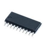
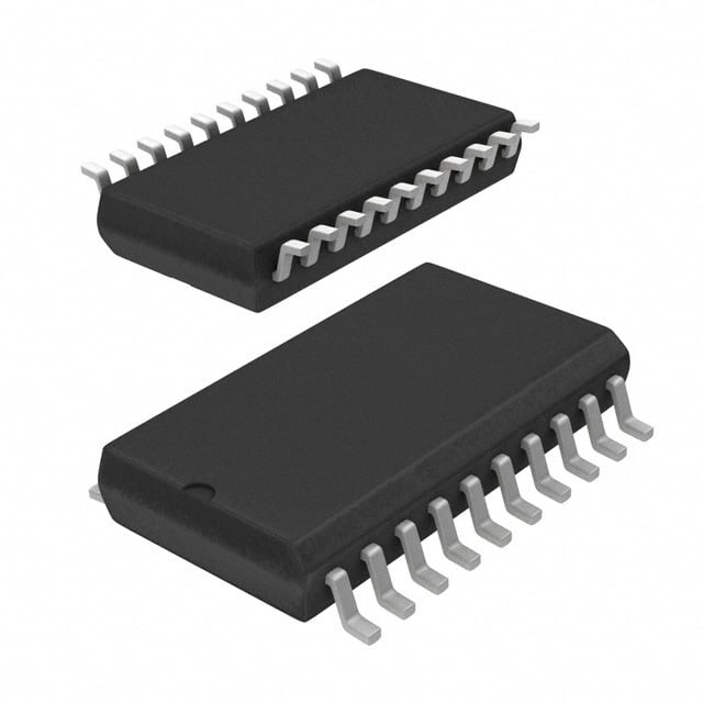
| 描述 | IC BUS TRANSCEIVER 8BIT 20SO总线收发器 Tri-State Octal Bus |
| 产品分类 | |
| 品牌 | Texas Instruments |
| 产品手册 | |
| 产品图片 |
|
| rohs | 符合RoHS无铅 / 符合限制有害物质指令(RoHS)规范要求 |
| 产品系列 | 逻辑集成电路,总线收发器,Texas Instruments SN74LV245ANSR74LV |
| 数据手册 | |
| 产品型号 | SN74LV245ANSR |
| 产品目录页面 | |
| 产品种类 | 总线收发器 |
| 传播延迟时间 | 15.9 ns |
| 低电平输出电流 | 16 mA |
| 供应商器件封装 | 20-SO |
| 元件数 | 1 |
| 其它名称 | 296-13231-1 |
| 功能 | Tri-State Octal Bus |
| 包装 | 剪切带 (CT) |
| 单位重量 | 266.700 mg |
| 商标 | Texas Instruments |
| 安装类型 | 表面贴装 |
| 安装风格 | SMD/SMT |
| 封装 | Reel |
| 封装/外壳 | 20-SOIC(0.209",5.30mm 宽) |
| 封装/箱体 | SOP-20 |
| 工作温度 | -40°C ~ 85°C |
| 工厂包装数量 | 2000 |
| 最大工作温度 | + 85 C |
| 最小工作温度 | - 40 C |
| 极性 | Non-Inverting |
| 标准包装 | 1 |
| 每元件位数 | 8 |
| 每芯片的通道数量 | 8 |
| 电压-电源 | 2 V ~ 5.5 V |
| 电流-输出高,低 | 16mA,16mA |
| 电源电压-最大 | 5.5 V |
| 电源电压-最小 | 2 V |
| 电路数量 | 8 |
| 系列 | SN74LV245A |
| 输入电平 | LVTTL |
| 输出电平 | LVTTL |
| 输出类型 | 3-State |
| 逻辑类型 | 收发器,非反相 |
| 逻辑系列 | LV-A |
| 高电平输出电流 | - 16 mA |


- 商务部:美国ITC正式对集成电路等产品启动337调查
- 曝三星4nm工艺存在良率问题 高通将骁龙8 Gen1或转产台积电
- 太阳诱电将投资9.5亿元在常州建新厂生产MLCC 预计2023年完工
- 英特尔发布欧洲新工厂建设计划 深化IDM 2.0 战略
- 台积电先进制程称霸业界 有大客户加持明年业绩稳了
- 达到5530亿美元!SIA预计今年全球半导体销售额将创下新高
- 英特尔拟将自动驾驶子公司Mobileye上市 估值或超500亿美元
- 三星加码芯片和SET,合并消费电子和移动部门,撤换高东真等 CEO
- 三星电子宣布重大人事变动 还合并消费电子和移动部门
- 海关总署:前11个月进口集成电路产品价值2.52万亿元 增长14.8%


PDF Datasheet 数据手册内容提取
Product Sample & Technical Tools & Support & Folder Buy Documents Software Community SN54LV245A,SN74LV245A SCLS382O–SEPTEMBER1997–REVISEDSEPTEMBER2014 SNx4LV245A Octal Bus Transceivers With 3-State Outputs 1 Features 2 Applications • 2-Vto5.5-VV Operation • Servers 1 CC • Maxt of6.5nsat5V • LEDDisplays pd • TypicalV (OutputGroundBounce) • NetworkSwitches OLP <0.8VatVCC=3.3V,TA=25°C • TelecomInfrastructure • TypicalVOHV(OutputVOH Undershoot) • MotorDrivers >2.3VatV =3.3V,T =25°C CC A • I/OExpanders • SupportMixed-ModeVoltageOperationonAll Ports 3 Description • I SupportsPartial-Power-DownModeOperation These octal bus transceivers are designed for 2-V to off • Latch-UpPerformanceExceeds250mAPer 5.5-VVCCoperation. JESD17 DeviceInformation • ESDProtectionExceedsJESD22 PARTNUMBER PACKAGE BODYSIZE(NOM) – 2000-VHuman-BodyModel(A114-A) SSOP(20) 7.20mm×5.30mm – 200-VMachineModel(A115-A) TVSOP(20) 5.00mm×4.40mm – 1000-VCharged-DeviceModel(C101) SNx4LV245A TSSOP(20) 6.50mm×4.40mm VQFN(20) 4.50mm×3.50mm SOIC(20) 12.80mm×7.50mm 4 Simplified Schematic DIR OE A1 B1 ToSevenOtherChannels 1 An IMPORTANT NOTICE at the end of this data sheet addresses availability, warranty, changes, use in safety-critical applications, intellectualpropertymattersandotherimportantdisclaimers.UNLESSOTHERWISENOTED,thisdocumentcontainsPRODUCTION DATA.
SN54LV245A,SN74LV245A SCLS382O–SEPTEMBER1997–REVISEDSEPTEMBER2014 www.ti.com Table of Contents 1 Features.................................................................. 1 9 DetailedDescription............................................ 11 2 Applications........................................................... 1 9.1 Overview.................................................................11 3 Description............................................................. 1 9.2 FunctionalBlockDiagram.......................................11 4 SimplifiedSchematic............................................. 1 9.3 FeatureDescription.................................................11 9.4 DeviceFunctionalModes........................................11 5 RevisionHistory..................................................... 2 10 ApplicationandImplementation........................ 12 6 PinConfigurationandFunctions......................... 3 10.1 ApplicationInformation..........................................12 7 Specifications......................................................... 5 10.2 TypicalApplication ...............................................12 7.1 AbsoluteMaximumRatings......................................5 11 PowerSupplyRecommendations..................... 13 7.2 HandlingRatings.......................................................5 12 Layout................................................................... 13 7.3 RecommendedOperatingConditions.......................6 7.4 ThermalInformation..................................................6 12.1 LayoutGuidelines.................................................13 7.5 ElectricalCharacteristics...........................................7 12.2 LayoutExample....................................................13 7.6 SwitchingCharacteristics,V =2.5V±0.2V........7 13 DeviceandDocumentationSupport................. 14 CC 7.7 SwitchingCharacteristics,V =3.3V±0.3V........8 13.1 RelatedLinks........................................................14 CC 7.8 SwitchingCharacteristics,V =5V±0.5V...........8 13.2 Trademarks...........................................................14 CC 7.9 NoiseCharacteristics................................................8 13.3 ElectrostaticDischargeCaution............................14 7.10 OperatingCharacteristics........................................8 13.4 Glossary................................................................14 7.11 TypicalCharacteristics............................................9 14 Mechanical,Packaging,andOrderable Information........................................................... 14 8 ParameterMeasurementInformation................10 5 Revision History ChangesfromRevisionN(August2012)toRevisionO Page • UpdateddocumenttonewTIdatasheetformat.................................................................................................................... 1 • DeletedOrderingInformationtable........................................................................................................................................ 1 • AddedApplications................................................................................................................................................................. 1 • AddedDeviceInformationtable............................................................................................................................................. 1 • AddedPinFunctionstable...................................................................................................................................................... 3 • AddedHandlingRatingstable................................................................................................................................................ 5 • ChangedMAXoperatingtemperatureto125°CinRecommendedOperatingConditionstable. ......................................... 6 • Added–40°Cto125°CforSN74LV245AinElectricalCharacteristicstable.......................................................................... 7 • Added–40°Cto125°CforSN74LV245AinallthreeSwitchingCharacteristicstables......................................................... 7 • AddedTypicalCharacteristics................................................................................................................................................ 9 • AddedDetailedDescriptionsection...................................................................................................................................... 11 • AddedApplicationandImplementationsection.................................................................................................................... 12 • AddedPowerSupplyRecommendationsandLayoutsections............................................................................................ 13 2 SubmitDocumentationFeedback Copyright©1997–2014,TexasInstrumentsIncorporated ProductFolderLinks:SN54LV245A SN74LV245A
SN54LV245A,SN74LV245A www.ti.com SCLS382O–SEPTEMBER1997–REVISEDSEPTEMBER2014 6 Pin Configuration and Functions SN54LV245A...JORWPACKAGE SN74LV245A...RGYPACKAGE SN54LV245A...FKPACKAGE SN74LV245A...DB,DGV,DW,NS, (TOPVIEW) (TOPVIEW) OR(PTOWPPVAICEKWA)GE DIR VCC A2 A1 DIRVCCOE DAIR1 12 2109 VOCEC A1 2 1 20 19 OE A3 4 3 2 1 20 1918 B1 A2 3 18 B1 A2 3 18 B1 A4 5 17 B2 A3 4 17 B2 A3 4 17 B2 A5 6 16 B3 A4 5 16 B3 A4 5 16 B3 A6 7 15 B4 A5 6 15 B4 A5 6 15 B4 A7 8 9 10 11 12 1314 B5 A6 7 14 B5 A6 7 14 B5 A7 8 13 B6 A7 8 13 B6 8 D 87 6 A N BB B A8 9 12 B7 A8 9 12 B7 G GND 10 11 B8 10 11 D 8 N B G PinFunctions PIN I/O DESCRIPTION NO. NAME 1 DIR I DirectionPin 2 A1 I/O A1I/O 3 A2 I/O A2I/O 4 A3 I/O A3I/O 5 A4 I/O A4I/O 6 A5 I/O A5I/O 7 A6 I/O A6I/O 8 A7 I/O A7I/O 9 A8 I/O A8I/O 10 GND — GroundPin 11 B8 I/O B8I/O 12 B7 I/O B7I/O 13 B6 I/O B6I/O 14 B5 I/O B5I/O 15 B4 I/O B4I/O 16 B3 I/O B3I/O 17 B2 I/O B2I/O 18 B1 I/O B1I/O 19 OE I OutputEnable 20 V — PowerPin CC Copyright©1997–2014,TexasInstrumentsIncorporated SubmitDocumentationFeedback 3 ProductFolderLinks:SN54LV245A SN74LV245A
SN54LV245A,SN74LV245A SCLS382O–SEPTEMBER1997–REVISEDSEPTEMBER2014 www.ti.com GQNPACKAGE (TOPVIEW) Pin Assignments 1 2 3 4 1 2 3 4 A A A1 DIR VCC OE B B A3 B2 A2 B1 C C A5 A4 B4 B3 D A7 B6 A6 B5 D E GND A8 B8 B7 E 4 SubmitDocumentationFeedback Copyright©1997–2014,TexasInstrumentsIncorporated ProductFolderLinks:SN54LV245A SN74LV245A
SN54LV245A,SN74LV245A www.ti.com SCLS382O–SEPTEMBER1997–REVISEDSEPTEMBER2014 7 Specifications 7.1 Absolute Maximum Ratings overoperatingfree-airtemperaturerange(unlessotherwisenoted)(1) MIN MAX UNIT V Supplyvoltagerange –0.5 7 V CC ExceptI/Oports(2) –0.5 7 V Inputvoltagerange V I I/Oports(2)(3) –0.5 7 V Voltagerangeappliedtoanyoutputinthehigh-impedanceorpower-offstate(2) –0.5 7 V O V Outputvoltagerangeappliedinthehighorlowstate(2)(3) –0.5 V +0.5 V O CC I Inputclampcurrent V <0 –20 mA IK I I Outputclampcurrent V <0 –50 mA OK O I Continuousoutputcurrent V =0toV ±35 mA O O CC ContinuouscurrentthroughV orGND ±70 mA CC (1) StressesbeyondthoselistedunderAbsoluteMaximumRatingsmaycausepermanentdamagetothedevice.Thesearestressratings only,andfunctionaloperationofthedeviceattheseoranyotherconditionsbeyondthoseindicatedunderRecommendedOperating Conditionsisnotimplied.Exposuretoabsolute-maximum-ratedconditionsforextendedperiodsmayaffectdevicereliability. (2) Theinputandoutputnegative-voltageratingsmaybeexceedediftheinputandoutputcurrentratingsareobserved. (3) Thisvalueislimitedto5.5-Vmaximum. 7.2 Handling Ratings MIN MAX UNIT T Storagetemperaturerange –65 150 °C stg Humanbodymodel(HBM),perANSI/ESDA/JEDECJS-001,all pins(1) 0 2000 V Electrostaticdischarge V (ESD) Chargeddevicemodel(CDM),perJEDECspecification JESD22-C101,allpins(2) 0 1000 (1) JEDECdocumentJEP155statesthat500-VHBMallowssafemanufacturingwithastandardESDcontrolprocess. (2) JEDECdocumentJEP157statesthat250-VCDMallowssafemanufacturingwithastandardESDcontrolprocess. Copyright©1997–2014,TexasInstrumentsIncorporated SubmitDocumentationFeedback 5 ProductFolderLinks:SN54LV245A SN74LV245A
SN54LV245A,SN74LV245A SCLS382O–SEPTEMBER1997–REVISEDSEPTEMBER2014 www.ti.com 7.3 Recommended Operating Conditions overoperatingfree-airtemperaturerange(unlessotherwisenoted)(1) SN54LV245A(2) SN74LV245A UNIT MIN MAX MIN MAX V Supplyvoltage 2 5.5 2 5.5 V CC V =2V 1.5 1.5 CC V =2.3Vto2.7V V ×0.7 V ×0.7 CC CC CC V High-levelinputvoltage V IH V =3Vto3.6V V ×0.7 V ×0.7 CC CC CC V =4.5Vto5.5V V ×0.7 V ×0.7 CC CC CC V =2V 0.5 0.5 CC V =2.3Vto2.7V V ×0.3 V ×0.3 CC CC CC V Low-levelinputvoltage V IL V =3Vto3.6V V ×0.3 V ×0.3 CC CC CC V =4.5Vto5.5V V ×0.3 V ×0.3 CC CC CC V Inputvoltage 0 5.5 0 5.5 V I Highorlowstate 0 V 0 V CC CC V Outputvoltage V O 3-state 0 5.5 0 5.5 V =2V –50 –50 µA CC V =2.3Vto2.7V –2 –2 CC I High-leveloutputcurrent OH V =3Vto3.6V –8 –8 mA CC V =4.5Vto5.5V –16 –16 CC V =2V 50 50 µA CC V =2.3Vto2.7V 2 2 CC I Low-leveloutputcurrent OL V =3Vto3.6V 8 8 mA CC V =4.5Vto5.5V 16 16 CC V =2.3Vto2.7V 200 200 CC Δt/Δv Inputtransitionriseorfallrate V =3Vto3.6V 100 100 ns/V CC V =4.5Vto5.5V 20 20 CC T Operatingfree-airtemperature –55 125 –40 125 °C A (1) AllunusedinputsofthedevicemustbeheldatV orGNDtoensureproperdeviceoperation.RefertotheTIapplicationreport, CC ImplicationsofSloworFloatingCMOSInputs(SCBA004). (2) ProductPreview 7.4 Thermal Information SN74LV245A THERMALMETRIC(1) DB DGV DW NS PW RGY UNIT 20PINS R Junction-to-ambientthermalresistance 94.6 114.8 77.5 76.6 101.5 34.1 θJA R Junction-to-case(top)thermalresistance 56.3 30.1 43.7 43.0 35.6 38.4 θJC(top) R Junction-to-boardthermalresistance 49.8 56.3 45.1 44.1 52.5 12.0 θJB ψJT Junction-to-topcharacterizationparameter 18.3 0.9 16.9 16.7 2.2 0.8 °C/W ψ Junction-to-boardcharacterization JB 49.4 55.6 44.7 43.7 52.0 12.0 parameter R Junction-to-case(bottom)thermal θJC(bot) — — — — — 7.1 resistance (1) Formoreinformationabouttraditionalandnewthermalmetrics,seetheICPackageThermalMetricsapplicationreport(SPRA953). 6 SubmitDocumentationFeedback Copyright©1997–2014,TexasInstrumentsIncorporated ProductFolderLinks:SN54LV245A SN74LV245A
SN54LV245A,SN74LV245A www.ti.com SCLS382O–SEPTEMBER1997–REVISEDSEPTEMBER2014 7.5 Electrical Characteristics overrecommendedoperatingfree-airtemperaturerange(unlessotherwisenoted) SN54LV245A(1) –40°Cto85°C –40°Cto125°C PARAMETER TESTCONDITIONS VCC SN74LV245A SN74LV245A UNIT MIN TYP MAX MIN TYP MAX MIN TYP MAX 2Vto IOH=–50µA 5.5V VCC–0.1 VCC–0.1 VCC–0.1 VOH IOH=–2mA 2.3V 2 2 2 V IOH=–8mA 3V 2.48 2.48 2.48 IOH=–16mA 4.5V 3.8 3.8 3.8 2Vto IOL=50µA 5.5V 0.1 0.1 0.1 VOL IOL=2mA 2.3V 0.4 0.4 0.4 V IOL=8mA 3V 0.44 0.44 0.44 IOL=16mA 4.5V 0.55 0.55 0.55 0to II Controlinputs VI=5.5VorGND 5.5V ±1 ±1 ±1 µA IOZ AorBport VO=VCCorGND 5.5V ±5 ±5 ±5 µA ICC VI=VCCorGND, IO=0 5.5V 20 20 20 µA Ioff VIorVO=0to5.5V 0 5 5 5 µA 3.3V 3 3 Ci Controlinputs VI=VCCorGND pF 5V 3 3 3.3V 5.5 5.5 Cio AorBport VO=VCCorGND pF 5V 5.5 5.5 (1) ProductPreview 7.6 Switching Characteristics, V = 2.5 V ± 0.2 V CC overrecommendedoperatingfree-airtemperaturerange(unlessotherwisenoted)(seeFigure3) PARAMETER FROM TO LOAD TA=25°C SN54LV245A(1) SN74LV245A –S40N°7C4LtoV214255A°C UNIT (INPUT) (OUTPUT) CAPACITANCE MIN TYP MAX MIN MAX MIN MAX MIN MAX tpd AorB BorA 8.3(2) 13(2) 1(2) 15(2) 1 15 1 17 ten OE AorB CL=15pF 11.8(2) 19.9(2) 1(2) 22(2) 1 22 1 24 ns tdis OE AorB 11.8(2) 18.1(2) 1(2) 20(2) 1 20 1 22 tpd AorB BorA 11.2 15.9 1 18 1 18 1 21 ten OE AorB 14.1 22.7 1 26 1 26 1 28 CL=50pF ns tdis OE AorB 17.6 23.1 1 25 1 25 1 27 tsk(o) 2 2 (1) ProductPreview (2) OnproductscomplianttoMIL-PRF-38535,thisparameterisnotproductiontested. Copyright©1997–2014,TexasInstrumentsIncorporated SubmitDocumentationFeedback 7 ProductFolderLinks:SN54LV245A SN74LV245A
SN54LV245A,SN74LV245A SCLS382O–SEPTEMBER1997–REVISEDSEPTEMBER2014 www.ti.com 7.7 Switching Characteristics, V = 3.3 V ± 0.3 V CC overrecommendedoperatingfree-airtemperaturerange(unlessotherwisenoted)(seeFigure3) PARAMETER FROM TO LOAD TA=25°C SN54LV245A(1) SN74LV245A –S40N°7C4LtoV214255A°C UNIT (INPUT) (OUTPUT) CAPACITANCE MIN TYP MAX MIN MAX MIN MAX MIN MAX tpd AorB BorA 5.9(2) 8.4(2) 1(2) 10(2) 1 10 1 11 ten OE AorB CL=15pF 8.2(2) 13.2(2) 1(2) 15.5(2) 1 15.5 1 16.5 ns tdis OE AorB 9.6(2) 16.5(2) 1(2) 19.5(2) 1 19.5 1 20.5 tpd AorB BorA 7.9 11.9 1 13.5 1 13.5 1 14.5 ten OE AorB 9.9 16.7 1 19 1 19 1 20 CL=50pF ns tdis OE AorB 13.9 19.8 1 22 1 22 1 23 tsk(o) 1.5 1.5 (1) ProductPreview (2) OnproductscomplianttoMIL-PRF-38535,thisparameterisnotproductiontested. 7.8 Switching Characteristics, V = 5 V ± 0.5 V CC overrecommendedoperatingfree-airtemperaturerange(unlessotherwisenoted)(seeFigure3) PARAMETER FROM TO LOAD TA=25°C SN54LV245A(1) SN74LV245A –S40N°7C4LtoV214255A°C UNIT (INPUT) (OUTPUT) CAPACITANCE MIN TYP MAX MIN MAX MIN MAX MIN MAX tpd AorB BorA 4.3(2) 5.5(2) 1(2) 6.5(2) 1 6.5 1 7 ten OE AorB CL=15pF 5.7(2) 8.5(2) 1(2) 10.6(2) 1 10 1 10.5 ns tdis OE AorB 7.8(2) 12.8(2) 1(2) 14.7(2) 1 14.2 1 14.7 tpd AorB BorA 5.6 7.5 1 8.5 1 8.5 1 9 ten OE AorB 7 10.6 1 12 1 12 1 12.5 CL=50pF ns tdis OE AorB 10.9 14.7 1 16 1 16 1 16.5 tsk(o) 1 1 (1) ProductPreview (2) OnproductscomplianttoMIL-PRF-38535,thisparameterisnotproductiontested. 7.9 Noise Characteristics(1) V =3.3V,C =50pF,T =25°C CC L A SN74LV245A PARAMETER UNIT MIN TYP MAX V Quietoutput,maximumdynamicV 0.5 0.8 V OL(P) OL V Quietoutput,minimumdynamicV –0.4 –0.8 V OL(V) OL V Quietoutput,minimumdynamicV 2.9 V OH(V) OH V High-leveldynamicinputvoltage 2.31 V IH(D) V Low-leveldynamicinputvoltage 0.99 V IL(D) (1) Characteristicsareforsurface-mountpackagesonly. 7.10 Operating Characteristics T =25°C A PARAMETER TESTCONDITIONS V TYP UNIT CC 3.3V 20 C Powerdissipationcapacitance Outputsenabled C =50pF, f=10MHz pF pd L 5V 25 8 SubmitDocumentationFeedback Copyright©1997–2014,TexasInstrumentsIncorporated ProductFolderLinks:SN54LV245A SN74LV245A
SN54LV245A,SN74LV245A www.ti.com SCLS382O–SEPTEMBER1997–REVISEDSEPTEMBER2014 7.11 Typical Characteristics 10 14 TPD in ns TPD in ns 12 8 10 s) 6 s) 8 n n D ( D ( P P 6 T 4 T 4 2 2 0 0 -100 -50 0 50 100 150 0 1 2 3 4 5 6 Temperature qC) D001 VCC D001 Figure1.TPDvsTemperatureat3.3V Figure2.TPDvsV CC Copyright©1997–2014,TexasInstrumentsIncorporated SubmitDocumentationFeedback 9 ProductFolderLinks:SN54LV245A SN74LV245A
SN54LV245A,SN74LV245A SCLS382O–SEPTEMBER1997–REVISEDSEPTEMBER2014 www.ti.com 8 Parameter Measurement Information VCC FromOutput Test FromOutput RL=1kΩ S1 Open TEST S1 UnderTest Point UnderTest GND tPLH/tPHL Open CL CL tPLZ/tPZL VCC (seeNoteA) (seeNoteA) tPHZ/tPZH GND OpenDrain VCC LOADCIRCUITFOR LOADCIRCUITFOR TOTEM-POLEOUTPUTS 3-STATEANDOPEN-DRAINOUTPUTS VCC TimingInput 50%VCC tw th 0V VCC tsu VCC Input 50%VCC 50%VCC DataInput 50%VCC 50%VCC 0V 0 V VOLTAGEWAVEFORMS VOLTAGEWAVEFORMS PULSEDURATION SETUPANDHOLDTIMES VCC Output VCC Input 50%VCC 50%VCC Control 50%VCC 50%VCC 0 V 0 V tPLH tPHL tPZL tPLZ Output In-Phase VOH Waveform1 ≈VCC Output 50%VCC 50%VCVCOL (seSe1NaotteVCBC) 50%VCC VOL+0.3VVOL tPHL tPLH tPZH tPHZ Output Out-of-OPuhtapsuet 50%VCC 50%VCVCOH WSa1veaftoGrmND2 50%VCC VOH–0.3VVOH VOL (seeNoteB) ≈0V VOLTAGEWAVEFORMS VOLTAGEWAVEFORMS PROPAGATIONDELAYTIMES ENABLEANDDISABLETIMES INVERTINGANDNONINVERTINGOUTPUTS LOW-ANDHIGH-LEVELENABLING NOTES: A. CLincludesprobeandjigcapacitance. B. Waveform1isforanoutputwithinternalconditionssuchthattheoutputislow,exceptwhendisabledbytheoutputcontrol. Waveform2isforanoutputwithinternalconditionssuchthattheoutputishigh,exceptwhendisabledbytheoutputcontrol. C. Allinputpulsesaresuppliedbygeneratorshavingthefollowingcharacteristics: PRR≤1MHz,ZO=50Ω,tr≤3ns,tf≤3ns. D. Theoutputsaremeasuredoneatatime,withoneinputtransitionpermeasurement. E. tPLZandtPHZarethesameastdis. F. tPZLandtPZHarethesameasten. G. tPHLandtPLHarethesameastpd. H. Allparametersandwaveformsarenotapplicabletoalldevices. Figure3. LoadCircuitandVoltageWaveforms 10 SubmitDocumentationFeedback Copyright©1997–2014,TexasInstrumentsIncorporated ProductFolderLinks:SN54LV245A SN74LV245A
SN54LV245A,SN74LV245A www.ti.com SCLS382O–SEPTEMBER1997–REVISEDSEPTEMBER2014 9 Detailed Description 9.1 Overview The SNx4LV245A devices are designed for asynchronous communication between data buses. The device transmits data from the A bus to the B bus or from the B bus to the A bus, depending on the logic level at the direction-control (DIR) input. The output-enable (OE) input can be used to disable the device so the buses are effectivelyisolated. To ensure the high-impedance state during power up or power down, OE should be tied to V through a pullup CC resistor;theminimumvalueoftheresistorisdeterminedbythecurrent-sinkingcapabilityofthedriver. These devices are fully specified for partial-power-down applications using I . The I circuitry disables the off off outputs,preventingdamagingcurrentbackflowthroughthedeviceswhentheyarepowereddown. 9.2 Functional Block Diagram DIR OE A1 B1 ToSevenOtherChannels Figure4. LogicDiagram(PositiveLogic) 9.3 Feature Description • Allowsdownvoltagetranslationfrom5Vto3.3V – Inputsacceptvoltagelevelsupto5.5V • Slowedgeratesminimizeoutputringing 9.4 Device Functional Modes Table1.FunctionTable INPUTS OPERATION OE DIR L L BdatatoAbus L H AdatatoBbus H X Isolation Copyright©1997–2014,TexasInstrumentsIncorporated SubmitDocumentationFeedback 11 ProductFolderLinks:SN54LV245A SN74LV245A
SN54LV245A,SN74LV245A SCLS382O–SEPTEMBER1997–REVISEDSEPTEMBER2014 www.ti.com 10 Application and Implementation 10.1 Application Information The SNx4LV245A is a low-drive CMOS device that can be used for a multitude of bus-interface type applications where output ringing is a concern. The low drive and slow edge rates will minimize overshoot and undershoot on the outputs. The inputs can accept voltages to 5.5 V at any valid V making the device ideal for down CC translation. 10.2 Typical Application Regulated 5 V Regulated 5 V OE VCC OE VCC DIR DIR A1 B1 A1 B1 µC 5-sVy sLtoEermD os tb,h oreearlradyss, A8 B8 3o.r3 -oVth µeCr 5s-Vys LtoeErm Do tsbh,o erarerladyss A8 B8 5-V LoEr DµoCtsh, errelays GND system boards GND system boards Figure5. TypicalApplicationSchematic 10.2.1 DesignRequirements This device uses CMOS technology and has balanced output drive. Care should be taken to avoid bus contention, because it can drive currents that would exceed maximum limits. Outputs can be combined to produce higher drive, but the high drive will also create faster edges into light loads; therefore, routing and load conditionsshouldbeconsideredtopreventringing. 10.2.2 DetailedDesignProcedure 1. RecommendedInputConditions: – Risetimeandfalltimespecifications,see(Δt/ΔV)inRecommendedOperatingConditions table. – Specifiedhighandlowlevels,see(V andV )inRecommendedOperatingConditions table. IH IL – Inputsareovervoltagetolerant,allowingthemtogoashighas5.5VatanyvalidV . CC 2. RecommendOutputConditions: – Loadcurrentsshouldnotexceed35mAperoutputand70mAtotalforthepart. – OutputsshouldnotbepulledaboveV . CC 12 SubmitDocumentationFeedback Copyright©1997–2014,TexasInstrumentsIncorporated ProductFolderLinks:SN54LV245A SN74LV245A
SN54LV245A,SN74LV245A www.ti.com SCLS382O–SEPTEMBER1997–REVISEDSEPTEMBER2014 Typical Application (continued) 10.2.3 ApplicationCurves AC245 HC245 LV245 LV Figure6.SwitchingCharacteristicsComparison 11 Power Supply Recommendations The power supply can be any voltage between the Min and Max supply voltage rating located in the RecommendedOperatingConditionstable. Each V terminal should have a good bypass capacitor to prevent power disturbance. For devices with a single CC supply,0.1μFisrecommendedandiftherearemultipleV terminalsthen0.01 μFor0.022 μFisrecommended CC for each power terminal. It is acceptable to parallel multiple bypass caps to reject different frequencies of noise. A 0.1 μF and 1 μF are commonly used in parallel. The bypass capacitor should be installed as close to the powerterminalaspossibleforbestresults. 12 Layout 12.1 Layout Guidelines Whenusingmultiplebitlogicdevicesinputsshouldnoteverfloat. In many cases, functions or parts of functions of digital logic devices are unused, for example, when only two inputs of a triple-input AND gate are used or only 3 of the 4 buffer gates are used. Such input pins should not be left unconnected because the undefined voltages at the outside connections result in undefined operational states. Specified in Figure 7 are the rules that must be observed under all circumstances. All unused inputs of digital logic devices must be connected to a high or low bias to prevent them from floating. The logic level that should be applied to any particular unused input depends on the function of the device. Generally they will be tied to GND or V , whichever makes more sense or is more convenient. It is generally acceptable to float CC outputs unless the part is a transceiver. If the transceiver has an output enable pin, it will disable the outputs section of the part when asserted. This will not disable the input section of the I/Os so they cannot float when disabled. 12.2 Layout Example V cc Input Unused Input Output Unused Input Output Input Figure7. LayoutDiagram Copyright©1997–2014,TexasInstrumentsIncorporated SubmitDocumentationFeedback 13 ProductFolderLinks:SN54LV245A SN74LV245A
SN54LV245A,SN74LV245A SCLS382O–SEPTEMBER1997–REVISEDSEPTEMBER2014 www.ti.com 13 Device and Documentation Support 13.1 Related Links The table below lists quick access links. Categories include technical documents, support and community resources,toolsandsoftware,andquickaccesstosampleorbuy. Table2.RelatedLinks TECHNICAL TOOLS& SUPPORT& PARTS PRODUCTFOLDER SAMPLE&BUY DOCUMENTS SOFTWARE COMMUNITY SN54LV245A Clickhere Clickhere Clickhere Clickhere Clickhere SN74LV245A Clickhere Clickhere Clickhere Clickhere Clickhere 13.2 Trademarks Alltrademarksarethepropertyoftheirrespectiveowners. 13.3 Electrostatic Discharge Caution Thesedeviceshavelimitedbuilt-inESDprotection.Theleadsshouldbeshortedtogetherorthedeviceplacedinconductivefoam duringstorageorhandlingtopreventelectrostaticdamagetotheMOSgates. 13.4 Glossary SLYZ022—TIGlossary. Thisglossarylistsandexplainsterms,acronyms,anddefinitions. 14 Mechanical, Packaging, and Orderable Information The following pages include mechanical, packaging, and orderable information. This information is the most current data available for the designated devices. This data is subject to change without notice and revision of thisdocument.Forbrowser-basedversionsofthisdatasheet,refertotheleft-handnavigation. 14 SubmitDocumentationFeedback Copyright©1997–2014,TexasInstrumentsIncorporated ProductFolderLinks:SN54LV245A SN74LV245A
PACKAGE OPTION ADDENDUM www.ti.com 24-Aug-2018 PACKAGING INFORMATION Orderable Device Status Package Type Package Pins Package Eco Plan Lead/Ball Finish MSL Peak Temp Op Temp (°C) Device Marking Samples (1) Drawing Qty (2) (6) (3) (4/5) SN74LV245ADBR ACTIVE SSOP DB 20 2000 Green (RoHS CU NIPDAU Level-1-260C-UNLIM -40 to 125 LV245A & no Sb/Br) SN74LV245ADGVR ACTIVE TVSOP DGV 20 2000 Green (RoHS CU NIPDAU Level-1-260C-UNLIM -40 to 125 LV245A & no Sb/Br) SN74LV245ADW ACTIVE SOIC DW 20 25 Green (RoHS CU NIPDAU Level-1-260C-UNLIM -40 to 125 LV245A & no Sb/Br) SN74LV245ADWE4 ACTIVE SOIC DW 20 25 Green (RoHS CU NIPDAU Level-1-260C-UNLIM -40 to 125 LV245A & no Sb/Br) SN74LV245ADWR ACTIVE SOIC DW 20 2000 Green (RoHS CU NIPDAU Level-1-260C-UNLIM -40 to 125 LV245A & no Sb/Br) SN74LV245ANSR ACTIVE SO NS 20 2000 Green (RoHS CU NIPDAU Level-1-260C-UNLIM -40 to 125 74LV245A & no Sb/Br) SN74LV245ANSRG4 ACTIVE SO NS 20 2000 Green (RoHS CU NIPDAU Level-1-260C-UNLIM -40 to 125 74LV245A & no Sb/Br) SN74LV245APW ACTIVE TSSOP PW 20 70 Green (RoHS CU NIPDAU Level-1-260C-UNLIM -40 to 125 LV245A & no Sb/Br) SN74LV245APWG4 ACTIVE TSSOP PW 20 70 Green (RoHS CU NIPDAU Level-1-260C-UNLIM -40 to 125 LV245A & no Sb/Br) SN74LV245APWR ACTIVE TSSOP PW 20 2000 Green (RoHS CU NIPDAU | CU SN Level-1-260C-UNLIM -40 to 125 LV245A & no Sb/Br) SN74LV245APWRE4 ACTIVE TSSOP PW 20 2000 Green (RoHS CU NIPDAU Level-1-260C-UNLIM -40 to 125 LV245A & no Sb/Br) SN74LV245APWRG3 ACTIVE TSSOP PW 20 2000 Green (RoHS CU SN Level-1-260C-UNLIM -40 to 125 LV245A & no Sb/Br) SN74LV245APWRG4 ACTIVE TSSOP PW 20 2000 Green (RoHS CU NIPDAU Level-1-260C-UNLIM -40 to 125 LV245A & no Sb/Br) SN74LV245ARGYR ACTIVE VQFN RGY 20 3000 Green (RoHS CU NIPDAU Level-2-260C-1 YEAR -40 to 125 LV245A & no Sb/Br) SN74LV245AZQNR ACTIVE BGA ZQN 20 1000 Green (RoHS SNAGCU Level-1-260C-UNLIM -40 to 85 LV245A MICROSTAR & no Sb/Br) JUNIOR (1) The marketing status values are defined as follows: ACTIVE: Product device recommended for new designs. LIFEBUY: TI has announced that the device will be discontinued, and a lifetime-buy period is in effect. Addendum-Page 1
PACKAGE OPTION ADDENDUM www.ti.com 24-Aug-2018 NRND: Not recommended for new designs. Device is in production to support existing customers, but TI does not recommend using this part in a new design. PREVIEW: Device has been announced but is not in production. Samples may or may not be available. OBSOLETE: TI has discontinued the production of the device. (2) RoHS: TI defines "RoHS" to mean semiconductor products that are compliant with the current EU RoHS requirements for all 10 RoHS substances, including the requirement that RoHS substance do not exceed 0.1% by weight in homogeneous materials. Where designed to be soldered at high temperatures, "RoHS" products are suitable for use in specified lead-free processes. TI may reference these types of products as "Pb-Free". RoHS Exempt: TI defines "RoHS Exempt" to mean products that contain lead but are compliant with EU RoHS pursuant to a specific EU RoHS exemption. Green: TI defines "Green" to mean the content of Chlorine (Cl) and Bromine (Br) based flame retardants meet JS709B low halogen requirements of <=1000ppm threshold. Antimony trioxide based flame retardants must also meet the <=1000ppm threshold requirement. (3) MSL, Peak Temp. - The Moisture Sensitivity Level rating according to the JEDEC industry standard classifications, and peak solder temperature. (4) There may be additional marking, which relates to the logo, the lot trace code information, or the environmental category on the device. (5) Multiple Device Markings will be inside parentheses. Only one Device Marking contained in parentheses and separated by a "~" will appear on a device. If a line is indented then it is a continuation of the previous line and the two combined represent the entire Device Marking for that device. (6) Lead/Ball Finish - Orderable Devices may have multiple material finish options. Finish options are separated by a vertical ruled line. Lead/Ball Finish values may wrap to two lines if the finish value exceeds the maximum column width. Important Information and Disclaimer:The information provided on this page represents TI's knowledge and belief as of the date that it is provided. TI bases its knowledge and belief on information provided by third parties, and makes no representation or warranty as to the accuracy of such information. Efforts are underway to better integrate information from third parties. TI has taken and continues to take reasonable steps to provide representative and accurate information but may not have conducted destructive testing or chemical analysis on incoming materials and chemicals. TI and TI suppliers consider certain information to be proprietary, and thus CAS numbers and other limited information may not be available for release. In no event shall TI's liability arising out of such information exceed the total purchase price of the TI part(s) at issue in this document sold by TI to Customer on an annual basis. Addendum-Page 2
PACKAGE MATERIALS INFORMATION www.ti.com 12-Feb-2019 TAPE AND REEL INFORMATION *Alldimensionsarenominal Device Package Package Pins SPQ Reel Reel A0 B0 K0 P1 W Pin1 Type Drawing Diameter Width (mm) (mm) (mm) (mm) (mm) Quadrant (mm) W1(mm) SN74LV245ADBR SSOP DB 20 2000 330.0 16.4 8.2 7.5 2.5 12.0 16.0 Q1 SN74LV245ADGVR TVSOP DGV 20 2000 330.0 12.4 6.9 5.6 1.6 8.0 12.0 Q1 SN74LV245ADWR SOIC DW 20 2000 330.0 24.4 10.8 13.3 2.7 12.0 24.0 Q1 SN74LV245ANSR SO NS 20 2000 330.0 24.4 8.4 13.0 2.5 12.0 24.0 Q1 SN74LV245APWR TSSOP PW 20 2000 330.0 16.4 6.95 7.1 1.6 8.0 16.0 Q1 SN74LV245APWRG3 TSSOP PW 20 2000 330.0 16.4 6.95 7.1 1.6 8.0 16.0 Q1 SN74LV245ARGYR VQFN RGY 20 3000 330.0 12.4 3.8 4.8 1.6 8.0 12.0 Q1 SN74LV245AZQNR BGAMI ZQN 20 1000 330.0 12.4 3.3 4.3 1.6 8.0 12.0 Q1 CROSTA RJUNI OR PackMaterials-Page1
PACKAGE MATERIALS INFORMATION www.ti.com 12-Feb-2019 *Alldimensionsarenominal Device PackageType PackageDrawing Pins SPQ Length(mm) Width(mm) Height(mm) SN74LV245ADBR SSOP DB 20 2000 367.0 367.0 38.0 SN74LV245ADGVR TVSOP DGV 20 2000 367.0 367.0 35.0 SN74LV245ADWR SOIC DW 20 2000 367.0 367.0 45.0 SN74LV245ANSR SO NS 20 2000 367.0 367.0 45.0 SN74LV245APWR TSSOP PW 20 2000 364.0 364.0 27.0 SN74LV245APWRG3 TSSOP PW 20 2000 364.0 364.0 27.0 SN74LV245ARGYR VQFN RGY 20 3000 367.0 367.0 35.0 SN74LV245AZQNR BGAMICROSTAR ZQN 20 1000 350.0 350.0 43.0 JUNIOR PackMaterials-Page2
None
None
None
None
None
MECHANICAL DATA MPDS006C – FEBRUARY 1996 – REVISED AUGUST 2000 DGV (R-PDSO-G**) PLASTIC SMALL-OUTLINE 24 PINS SHOWN 0,23 0,40 0,07 M 0,13 24 13 0,16 NOM 4,50 6,60 4,30 6,20 Gage Plane 0,25 0°–(cid:1)8° 0,75 1 12 0,50 A Seating Plane 0,15 1,20 MAX 0,08 0,05 PINS ** 14 16 20 24 38 48 56 DIM A MAX 3,70 3,70 5,10 5,10 7,90 9,80 11,40 A MIN 3,50 3,50 4,90 4,90 7,70 9,60 11,20 4073251/E 08/00 NOTES: A. All linear dimensions are in millimeters. B. This drawing is subject to change without notice. C. Body dimensions do not include mold flash or protrusion, not to exceed 0,15 per side. D. Falls within JEDEC: 24/48 Pins – MO-153 14/16/20/56 Pins – MO-194 • POST OFFICE BOX 655303 DALLAS, TEXAS 75265
None
None
PACKAGE OUTLINE DB0020A TSSOP - 2 mm max height SCALE 2.000 SMALL OUTLINE PACKAGE C 8.2 TYP 7.4 A 0.1 C PIN 1 INDEX AREA SEATING PLANE 18X 0.65 20 1 2X 7.5 5.85 6.9 NOTE 3 10 11 0.38 20X 0.22 5.6 B 0.1 C A B 5.0 NOTE 4 2 MAX (0.15) TYP 0.25 SEE DETAIL A GAGE PLANE 0 -8 0.95 0.05 MIN 0.55 DETA 15AIL A TYPICAL 4214851/A 12/2017 NOTES: 1. All linear dimensions are in millimeters. Any dimensions in parenthesis are for reference only. Dimensioning and tolerancing per ASME Y14.5M. 2. This drawing is subject to change without notice. 3. This dimension does not include mold flash, protrusions, or gate burrs. Mold flash, protrusions, or gate burrs shall not exceed 0.15 mm per side. 4. This dimension does not include interlead flash. Interlead flash shall not exceed 0.25 mm per side. 5. Reference JEDEC registration MO-150. www.ti.com
EXAMPLE BOARD LAYOUT DB0020A TSSOP - 2 mm max height SMALL OUTLINE PACKAGE 20X (1.85) SYMM (R0.05) TYP 1 20X (0.45) 20 SYMM 18X (0.65) 10 11 (7) LAND PATTERN EXAMPLE EXPOSED METAL SHOWN SCALE: 10X SOLDER MASK METAL METAL UNDER SOLDER MASK OPENING SOLDER MASK OPENING EXPOSED METAL EXPOSED METAL 0.07 MAX 0.07 MIN ALL AROUND ALL AROUND NON-SOLDER MASK SOLDER MASK DEFINED DEFINED (PREFERRED) SOLDE15.000 R MASK DETAILS 4214851/A 12/2017 NOTES: (continued) 6. Publication IPC-7351 may have alternate designs. 7. Solder mask tolerances between and around signal pads can vary based on board fabrication site. www.ti.com
EXAMPLE STENCIL DESIGN DB0020A TSSOP - 2 mm max height SMALL OUTLINE PACKAGE 20X (1.85) SYMM (R0.05) TYP 1 20X (0.45) 20 SYMM 18X (0.65) 10 11 (7) SOLDER PASTE EXAMPLE BASED ON 0.125 mm THICK STENCIL SCALE: 10X 4214851/A 12/2017 NOTES: (continued) 8. Laser cutting apertures with trapezoidal walls and rounded corners may offer better paste release. IPC-7525 may have alternate design recommendations. 9. Board assembly site may have different recommendations for stencil design. www.ti.com
PACKAGE OUTLINE DW0020A SOIC - 2.65 mm max height SCALE 1.200 SOIC C 10.63 SEATING PLANE TYP 9.97 A PIN 1 ID 0.1 C AREA 18X 1.27 20 1 13.0 2X 12.6 11.43 NOTE 3 10 11 0.51 20X 7.6 0.31 2.65 MAX B 7.4 0.25 C A B NOTE 4 0.33 TYP 0.10 0.25 SEE DETAIL A GAGE PLANE 0.3 1.27 0 - 8 0.1 0.40 DETAIL A TYPICAL 4220724/A 05/2016 NOTES: 1. All linear dimensions are in millimeters. Dimensions in parenthesis are for reference only. Dimensioning and tolerancing per ASME Y14.5M. 2. This drawing is subject to change without notice. 3. This dimension does not include mold flash, protrusions, or gate burrs. Mold flash, protrusions, or gate burrs shall not exceed 0.15 mm per side. 4. This dimension does not include interlead flash. Interlead flash shall not exceed 0.43 mm per side. 5. Reference JEDEC registration MS-013. www.ti.com
EXAMPLE BOARD LAYOUT DW0020A SOIC - 2.65 mm max height SOIC 20X (2) SYMM 1 20 20X (0.6) 18X (1.27) SYMM (R0.05) TYP 10 11 (9.3) LAND PATTERN EXAMPLE SCALE:6X SOOPLEDNEINRG MASK METAL MSOELTDAEL RU NMDAESRK SOOPLEDNEINRG MASK 0.07 MAX 0.07 MIN ALL AROUND ALL AROUND NON SOLDER MASK SOLDER MASK DEFINED DEFINED SOLDER MASK DETAILS 4220724/A 05/2016 NOTES: (continued) 6. Publication IPC-7351 may have alternate designs. 7. Solder mask tolerances between and around signal pads can vary based on board fabrication site. www.ti.com
EXAMPLE STENCIL DESIGN DW0020A SOIC - 2.65 mm max height SOIC 20X (2) SYMM 1 20 20X (0.6) 18X (1.27) SYMM 10 11 (9.3) SOLDER PASTE EXAMPLE BASED ON 0.125 mm THICK STENCIL SCALE:6X 4220724/A 05/2016 NOTES: (continued) 8. Laser cutting apertures with trapezoidal walls and rounded corners may offer better paste release. IPC-7525 may have alternate design recommendations. 9. Board assembly site may have different recommendations for stencil design. www.ti.com
IMPORTANTNOTICEANDDISCLAIMER TIPROVIDESTECHNICALANDRELIABILITYDATA(INCLUDINGDATASHEETS),DESIGNRESOURCES(INCLUDINGREFERENCE DESIGNS),APPLICATIONOROTHERDESIGNADVICE,WEBTOOLS,SAFETYINFORMATION,ANDOTHERRESOURCES“ASIS” ANDWITHALLFAULTS,ANDDISCLAIMSALLWARRANTIES,EXPRESSANDIMPLIED,INCLUDINGWITHOUTLIMITATIONANY IMPLIEDWARRANTIESOFMERCHANTABILITY,FITNESSFORAPARTICULARPURPOSEORNON-INFRINGEMENTOFTHIRD PARTYINTELLECTUALPROPERTYRIGHTS. TheseresourcesareintendedforskilleddevelopersdesigningwithTIproducts.Youaresolelyresponsiblefor(1)selectingtheappropriate TIproductsforyourapplication,(2)designing,validatingandtestingyourapplication,and(3)ensuringyourapplicationmeetsapplicable standards,andanyothersafety,security,orotherrequirements.Theseresourcesaresubjecttochangewithoutnotice.TIgrantsyou permissiontousetheseresourcesonlyfordevelopmentofanapplicationthatusestheTIproductsdescribedintheresource.Other reproductionanddisplayoftheseresourcesisprohibited.NolicenseisgrantedtoanyotherTIintellectualpropertyrightortoanythird partyintellectualpropertyright.TIdisclaimsresponsibilityfor,andyouwillfullyindemnifyTIanditsrepresentativesagainst,anyclaims, damages,costs,losses,andliabilitiesarisingoutofyouruseoftheseresources. TI’sproductsareprovidedsubjecttoTI’sTermsofSale(www.ti.com/legal/termsofsale.html)orotherapplicabletermsavailableeitheron ti.comorprovidedinconjunctionwithsuchTIproducts.TI’sprovisionoftheseresourcesdoesnotexpandorotherwisealterTI’sapplicable warrantiesorwarrantydisclaimersforTIproducts. MailingAddress:TexasInstruments,PostOfficeBox655303,Dallas,Texas75265 Copyright©2019,TexasInstrumentsIncorporated