ICGOO在线商城 > 集成电路(IC) > 逻辑 - 栅极和逆变器 > SN74LV1T86DCKR
 Datasheet下载
- 型号: SN74LV1T86DCKR
- 制造商: Texas Instruments
- 库位|库存: xxxx|xxxx
- 要求:
| 数量阶梯 | 香港交货 | 国内含税 |
| +xxxx | $xxxx | ¥xxxx |
查看当月历史价格
查看今年历史价格
SN74LV1T86DCKR产品简介:
ICGOO电子元器件商城为您提供SN74LV1T86DCKR由Texas Instruments设计生产,在icgoo商城现货销售,并且可以通过原厂、代理商等渠道进行代购。 SN74LV1T86DCKR价格参考¥0.91-¥2.61。Texas InstrumentsSN74LV1T86DCKR封装/规格:逻辑 - 栅极和逆变器, XOR (Exclusive OR) IC 1 Channel SC-70-5。您可以下载SN74LV1T86DCKR参考资料、Datasheet数据手册功能说明书,资料中有SN74LV1T86DCKR 详细功能的应用电路图电压和使用方法及教程。
SN74LV1T86DCKR 是由 Texas Instruments(德州仪器)生产的一款单通道 XOR(异或)逻辑门器件,属于逻辑 - 栅极和逆变器类别。该型号基于低电压 CMOS (LVCMOS) 技术设计,适用于多种数字电路应用。以下是其主要应用场景:

 1. 数字信号处理
   - SN74LV1T86DCKR 可用于实现基本的数字逻辑运算,例如比较两个输入信号是否不同。在需要对二进制数据进行简单逻辑判断时,这款 XOR 门非常适用。
   - 常见于编码/解码电路、奇偶校验生成与检测等场景。

 2. 时钟和同步电路
   - 在时钟信号生成或同步电路中,XOR 门可以用来产生相位差信号或检测时钟边沿变化。
   - 例如,通过将时钟信号与其延迟版本输入到 XOR 门中,可以生成脉冲宽度与延迟时间相关的信号。

 3. 模数转换和滤波
   - 在模拟信号数字化过程中,XOR 门可用于构建简单的调制解调器或混频器。
   - 它也可以作为频率合成器的一部分,用于调整输出信号的频率特性。

 4. 数据传输控制
   - 在数据通信系统中,XOR 门常用于实现数据加密或解密功能。例如,使用 XOR 操作对明文和密钥进行按位异或运算以生成密文。
   - 此外,它还可以用作数据选择器或切换开关,在多路复用器和解复用器设计中发挥重要作用。

 5. 电源管理与低功耗设计
   - 由于 SN74LV1T86DCKR 支持较低的工作电压范围(1.65V 至 5.5V),并且具有较低的静态电流消耗,因此非常适合便携式设备或电池供电系统的逻辑控制部分。

 6. 教育和实验平台
   - 这款器件因其简单易用且性能稳定,被广泛应用于教学实验室及电子爱好者项目中,帮助学生理解基础逻辑门的工作原理及其实际用途。

总之,SN74LV1T86DCKR 凭借其紧凑的封装形式(如 SC-70 或 SOT-353)、宽泛的工作电压范围以及出色的电气特性,成为许多现代电子产品开发中的理想选择。
| 参数 | 数值 |
| 产品目录 | 集成电路 (IC)半导体 |
| 描述 | IC GATE XOR 1CH 2-INP SC-70-5逻辑门 SGL Pwr Spply 2-IN EXCLSVE-OR GATE CMOS |
| 产品分类 | |
| 品牌 | Texas Instruments |
| 产品手册 | http://www.ti.com/litv/scls742a |
| 产品图片 | |
| rohs | 符合RoHS无铅 / 符合限制有害物质指令(RoHS)规范要求 |
| 产品系列 | 逻辑集成电路,逻辑门,Texas Instruments SN74LV1T86DCKR74LV |
| mouser_ship_limit | 该产品可能需要其他文档才能发货到中国。 |
| 数据手册 | |
| 产品型号 | SN74LV1T86DCKR |
| 不同V、最大CL时的最大传播延迟 | 7ns @ 5V, 30pF |
| 产品 | XOR |
| 产品种类 | 逻辑门 |
| 低电平输出电流 | 8 mA |
| 供应商器件封装 | SC-70-5 |
| 其它名称 | 296-37203-6 |
| 制造商产品页 | http://www.ti.com/general/docs/suppproductinfo.tsp?distId=10&orderablePartNumber=SN74LV1T86DCKR |
| 包装 | Digi-Reel® |
| 商标 | Texas Instruments |
| 安装类型 | 表面贴装 |
| 安装风格 | SMD/SMT |
| 封装 | Reel |
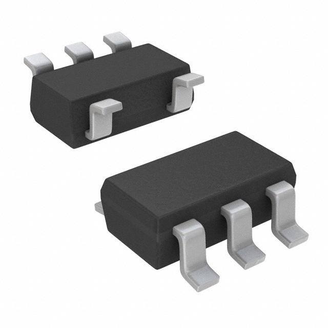
| 封装/外壳 | 6-TSSOP(5 引线),SC-88A,SOT-353 |
| 封装/箱体 | SC-70-5 |
| 工作温度 | -40°C ~ 125°C |
| 工作温度范围 | - 40 C to + 125 C |
| 工厂包装数量 | 3000 |
| 最大工作温度 | + 125 C |
| 最小工作温度 | - 40 C |
| 栅极数量 | 1 |
| 标准包装 | 1 |
| 特性 | - |
| 电压-电源 | 1.6 V ~ 5.5 V |
| 电流-输出高,低 | 8mA,8mA |
| 电流-静态(最大值) | 1µA |
| 电源电压-最大 | 5.5 V |
| 电源电压-最小 | 1.6 V |
| 电路数 | 1 |
| 系列 | SN74LV1T86 |
| 输入/输出线数量 | 2 / 1 |
| 输入数 | 2 |
| 输入线路数量 | 2 |
| 输出电流 | 8 mA |
| 输出线路数量 | 1 |
| 逻辑电平-低 | 0.58 V ~ 0.8 V |
| 逻辑电平-高 | 0.94 V ~ 2.1 V |
| 逻辑类型 | XOR(异或) |
| 逻辑系列 | 74LV |
| 高电平输出电流 | - 8 mA |


- 商务部:美国ITC正式对集成电路等产品启动337调查
- 曝三星4nm工艺存在良率问题 高通将骁龙8 Gen1或转产台积电
- 太阳诱电将投资9.5亿元在常州建新厂生产MLCC 预计2023年完工
- 英特尔发布欧洲新工厂建设计划 深化IDM 2.0 战略
- 台积电先进制程称霸业界 有大客户加持明年业绩稳了
- 达到5530亿美元!SIA预计今年全球半导体销售额将创下新高
- 英特尔拟将自动驾驶子公司Mobileye上市 估值或超500亿美元
- 三星加码芯片和SET,合并消费电子和移动部门,撤换高东真等 CEO
- 三星电子宣布重大人事变动 还合并消费电子和移动部门
- 海关总署:前11个月进口集成电路产品价值2.52万亿元 增长14.8%


PDF Datasheet 数据手册内容提取
Product Sample & Technical Tools & Support & Folder Buy Documents Software Community SN74LV1T86 SCLS742A–NOVMEBER2013–REVISEDFEBRUARY2014 SN74LV1T86 Single Power Supply 2-INput Exclusive-OR Gate CMOS Logic Level Shifter 1 Features 2 Applications • Single-SupplyVoltageTranslatorat • Industrialcontrollers 1 5.0/3.3/2.5/1.8VVCC • Telecom • OperatingRangeof1.8Vto5.5V • Portableapplications • UpTranslation • Servers – 1.2V(1)to1.8Vat1.8VVCC • PCandnotebooks – 1.5V(1)to2.5Vat2.5VVCC • Automotive – 1.8V(1)to3.3Vat3.3VV CC 3 Description – 3.3Vto5.0Vat5.0VV CC SN74LV1T86 is a low voltage CMOS gate logic that • DownTranslation operates at a wider voltage range for industrial, – 3.3Vto1.8Vat1.8VV CC portable, telecom, and automotive applications. The – 3.3Vto2.5Vat2.5VV output level is referenced to the supply voltage and is CC abletosupport1.8V/2.5V/3.3V/5VCMOSlevels. – 5.0Vto3.3Vat3.3VV CC • LogicOutputisReferencedtoV The input is designed with a lower threshold circuit to CC match1.8VinputlogicatV =3.3Vandcanbeused • OutputDrive CC in 1.8V to 3.3V level up translation. In addition, the – 8mAOutputDriveat5V 5V tolerant input pins enable down translation (e.g. – 7mAOutputDriveat3.3V 3.3V to 2.5V output at V = 2.5V). The wide V CC CC – 3mAOutputDriveat1.8V range of 1.8V to 5.5V allows generation of desired outputlevelstoconnecttocontrollersorprocessors. • Characterizedupto50MHzat3.3VV CC The SN74LV1T86 is designed with current-drive • 5VToleranceonInputPins capability of 8 mA to reduce line reflections, • –40°Cto125°COperatingTemperatureRange overshoot, and undershoot caused by high-drive • Pb-FreePackagesAvailable:SC-70(DCK) outputs. – 2 ×2.1 × 0.65mm(Height1.1mm) DeviceInformation • Latch-UpPerformanceExceeds250mA PerJESD17 ORDERNUMBER PACKAGE BODYSIZE SN74LV1T86DBVR SOT-23(5) 2,90mmx1,60mm • ESDPerformanceTestedPerJESD22 SN74LV1T86DCKR SC70(5) 2,00mmx1,25mm – 2000-VHuman-BodyModel (A114-B,ClassII) – 200-VMachineModel(A115-A) DCKorDBVPACKAGE (TOPVIEW) – 1000-VCharged-DeviceModel(C101) • SupportsStandardLogicPinouts A 1 5 V • CMOSOutputBCompatiblewithAUP1Gand CC LVC1GFamilies (1) RefertotheVIH/VILandoutputdriveforlowerVCCcondition. B 2 GND 3 4 Y 1 An IMPORTANT NOTICE at the end of this data sheet addresses availability, warranty, changes, use in safety-critical applications, intellectualpropertymattersandotherimportantdisclaimers.PRODUCTIONDATA.
SN74LV1T86 SCLS742A–NOVMEBER2013–REVISEDFEBRUARY2014 www.ti.com Table of Contents 1 Features ................................................................. 1 4.6 OperatingCharacteristics ........................................8 2 Applications .......................................................... 1 5 ParameterMeasurementInformation .................9 3 Description ............................................................ 1 5.1 MoreProductSelection............................................9 4 RevisionHistory ................................................... 2 6 DeviceandDocumentationSupport .................10 4.1 TypicalDesignExamples.........................................5 6.1 Trademarks ............................................................10 4.2 AbsoluteMaximumRatings .....................................6 6.2 ElectrostaticDischargeCaution.............................10 4.3 RecommendedOperatingConditions......................7 6.3 Glossary .................................................................10 4.4 ElectricalCharacteristics..........................................7 7 Mechanical,Packaging,andOrderable 4.5 SwitchingCharacteristics .........................................8 Information .......................................................... 10 4 Revision History NOTE:Pagenumbersforpreviousrevisionsmaydifferfrompagenumbersinthecurrentversion. ChangesfromOriginal(November2013)toRevisionA Page • Updateddocumentformatting. .............................................................................................................................................. 1 2 SubmitDocumentationFeedback Copyright©2013–2014,TexasInstrumentsIncorporated ProductFolderLinks:SN74LV1T86
SN74LV1T86 www.ti.com SCLS742A–NOVMEBER2013–REVISEDFEBRUARY2014 FunctionTable INPUT OUTPUT (LowerLevelInput) (V CMOS) CC A B Y L L L L H H H L H H H L SUPPLYV =3.3V CC A B Y V (min)=1.35V V (min)=2.9V IH OH V (max)=0.08V V (max)=0.2V IL OL Copyright©2013–2014,TexasInstrumentsIncorporated SubmitDocumentationFeedback 3 ProductFolderLinks:SN74LV1T86
SN74LV1T86 SCLS742A–NOVMEBER2013–REVISEDFEBRUARY2014 www.ti.com Figure1. ExcellentSignalIntegrity(1.8Vto3.3Vat3.3VV ) CC Figure2. ExcellentSignalIntegrity(3.3Vto3.3Vat3.3VV ) CC 4 SubmitDocumentationFeedback Copyright©2013–2014,TexasInstrumentsIncorporated ProductFolderLinks:SN74LV1T86
SN74LV1T86 www.ti.com SCLS742A–NOVMEBER2013–REVISEDFEBRUARY2014 Figure3. ExcellentSignalIntegrity(3.3Vto1.8Vat1.8VV ) CC 4.1 Typical Design Examples VIH= 2.0V VIH= 0.99V Vcc = 5.0V Vcc = 1.8V VIL= 0.8V VIL= 0.55V 5.0V, 3.3V 5.0V LV1Txx Logic 5.0V 2.5V, 1.8V LV1Txx Logic 1.8V 3.3V System 1.5V, 1.2V System System System Copyright©2013–2014,TexasInstrumentsIncorporated SubmitDocumentationFeedback 5 ProductFolderLinks:SN74LV1T86
SN74LV1T86 SCLS742A–NOVMEBER2013–REVISEDFEBRUARY2014 www.ti.com Typical Design Examples (continued) Vcc= 3.3V 5.0V, 3.3V LV1Txx Logic 3.3V 2.5V, 1.8V System System VOH min= 2.4V VIH min= 1.36V VOLmax= 0.4V VILmin= 0.8V Figure4. SwitchingThresholdsfor1.8-Vto3.3-VTranslation 4.2 Absolute Maximum Ratings(1) overoperatingfree-airtemperaturerange(unlessotherwisenoted) MIN MAX UNIT V Supplyvoltagerange –0.5 7.0 V CC V Inputvoltagerange(2) –0.5 7.0 V I Voltagerangeappliedtoanyoutputinthehigh-impedanceorpower-offstate(2) –0.5 4.6 V V O Voltagerangeappliedtoanyoutputinthehighorlowstate(2) –0.5 V +0.5 V CC I Inputclampcurrent V <0 –20 mA IK I I Outputclampcurrent V <0orV >V ±20 mA OK O O CC I ±25 mA O Continuousoutputcurrent ContinuouscurrentthroughV orGND ±50 mA CC DBVpackage 206 θ Packagethermalimpedance(3) JA DCKpackage 252 °C/W T Storagetemperaturerange –65 150 °C stg (1) Stressesbeyondthoselistedunder"absolutemaximumratings"maycausepermanentdamagetothedevice.Thesearestressratings only,andfunctionaloperationofthedeviceattheseoranyotherconditionsbeyondthoseindicatedunder"recommendedoperating conditions"isnotimplied.Exposuretoabsolute-maximum-ratedconditionsforextendedperiodsmayaffectdevicereliability. (2) Theinputnegative-voltageandoutputvoltageratingsmaybeexceedediftheinputandoutputcurrentratingsareobserved. (3) ThepackagethermalimpedanceiscalculatedinaccordancewithJESD51-7. 6 SubmitDocumentationFeedback Copyright©2013–2014,TexasInstrumentsIncorporated ProductFolderLinks:SN74LV1T86
SN74LV1T86 www.ti.com SCLS742A–NOVMEBER2013–REVISEDFEBRUARY2014 4.3 Recommended Operating Conditions(1) overoperatingfree-airtemperaturerange(unlessotherwisenoted) MIN MAX UNIT V Supplyvoltage 1.6 5.5 V CC V Inputvoltage 0 5.5 V I V Outputvoltage 0 V V O CC V =1.8V –3 CC V =2.5V –5 CC I High-leveloutputcurrent mA OH V =3.3V –7 CC V =5.0V –8 CC V =1.8V 3 CC V =2.5V 5 CC I Low-leveloutputcurrent mA OL V =3.3V 7 CC V =5.0V 8 CC V =1.8V 20 CC Δt/Δ Inputtransitionriseorfallrate V =3.3Vor2.5V 20 ns/V v CC V =5.0V 20 CC T Operatingfree-airtemperature –40 125 °C A (1) AllunusedinputsofthedevicemustbeheldatV orGNDtoensureproperdeviceoperation.RefertotheTIapplicationreport, CC ImplicationsofSloworFloatingCMOSInputs,literaturenumberSCBA004. 4.4 Electrical Characteristics overrecommendedoperatingfree-airtemperaturerange(unlessotherwisenoted) TA=25°C TA=–40°Cto125°C PARAMETER TESTCONDITIONS VCC UNIT MIN TYP MAX MIN MAX VCC=1.65Vto1.8V 0.94 1.0 VCC=2.0V 0.99 1.03 VCC=2.25Vto2.5V 1.135 1.18 High-levelinput VCC=2.75V 1.21 1.23 VIH voltage VCC=3Vto3.3V 1.35 1.37 V VCC=3.6V 1.47 1.48 VCC=4.5Vto5.0V 2.02 2.03 VCC=5.5V 2.1 2.11 VCC=1.65Vto2.0V 0.58 0.55 Low-levelinput VCC=2.25Vto2.75V 0.75 0.71 VIL voltage VCC=3Vto3.6V 0.8 0.65 V VCC=4.5Vto5.5V 0.8 0.8 IOH=–20µA 1.65Vto5.5V VCC–0.1 VCC–0.1 V 1.65V 1.28 1.21 IOH=–2.0mA V 1.8V 1.5 1.45 IOH=–2.3mA 2.0 2.0 2.3V V IOH=–3mA 2.0 1.93 IOH=–3mA 2.5V 2.25 2.15 V VOH IOH=–3.0mA 2.78 2.7 3.0V IOH=–5.5mA 2.6 2.49 V IOH=–5.5mA 3.3V 2.9 2.8 IOH=–4mA 4.2 4.1 4.5V IOH=–8mA 4.1 3.95 V IOH=–8mA 5.0V 4.6 4.5 Copyright©2013–2014,TexasInstrumentsIncorporated SubmitDocumentationFeedback 7 ProductFolderLinks:SN74LV1T86
SN74LV1T86 SCLS742A–NOVMEBER2013–REVISEDFEBRUARY2014 www.ti.com Electrical Characteristics (continued) overrecommendedoperatingfree-airtemperaturerange(unlessotherwisenoted) TA=25°C TA=–40°Cto125°C PARAMETER TESTCONDITIONS VCC UNIT MIN TYP MAX MIN MAX IOL=20µA 1.65Vto5.5V 0.1 0.1 IOL=1.9mA 1.65V 0.2 0.25 IOH=2.3mA 0.1 0.15 2.3V IOH=3mA 0.15 0.2 VOL IOL=3mA 0.1 0.15 3.0V IOL=5.5mA 0.2 0.252 V IOL=4mA 0.15 0.2 4.5V IOL=8mA 0.3 0.35 II Ainput VI=0VorVCC 0V,1.8V,2.5V,3.3V,5.5V 0.1 ±1 μA 5.0V 1 10 ICC VIOI==00;VopoernVoCnC,loading 32..35VV 11 1100 μA 1.8V 1 10 Oneinputat0.3Vor3.4V, Otherinputsat0orVCC, 5.5V 1.35 1.5 mA IO=0 ΔICC Oneinputat0.3Vor1.1V Otherinputsat0orVCC, 1.8V 10 10 μA IO=0 Ci VI=VCCorGND 3.3V 2 10 2 10 pF Co VO=VCCorGND 3.3V 2.5 2.5 pF 4.5 Switching Characteristics overrecommendedoperatingfree-airtemperaturerange(unlessotherwisenoted)(seeFigure7) FROM TO FREQUENCY TA=25°C TA=–65°Cto125°C PARAMETER V C UNIT (INPUT) (OUTPUT) (TYP) CC L MIN TYP MAX MIN TYP MAX 15pF 4 5 4 5 5.0V ns 30pF 5.5 7.0 5.5 7.0 DCto50MHz 15pF 4.8 5 5 5.5 3.3V ns 30pF 5 5.5 5.5 6.5 t AnyIn Y pd 15pF 6 6.5 7 7.5 DCto25MHz 2.5V ns 30pF 6.5 7.5 7.5 8.5 15pF 10.5 11 11 12 DCto15MHz 1.8V ns 30pF 12 13 12 14 4.6 Operating Characteristics T =25°C A PARAMETER TESTCONDITIONS V TYP UNIT CC 1.8V±0.15V 14 2.5V±0.2V 14 C Powerdissipationcapacitance f=1MHzand10MHz pF pd 3.3V±0.3V 14 5.5V±0.5V 14 8 SubmitDocumentationFeedback Copyright©2013–2014,TexasInstrumentsIncorporated ProductFolderLinks:SN74LV1T86
SN74LV1T86 www.ti.com SCLS742A–NOVMEBER2013–REVISEDFEBRUARY2014 5 Parameter Measurement Information From Output Under Test VCC = 2.5 V VCC = 3.3 V CL 1 MW ± 0.2 V ± 0.3 V (see Note A) CL 5, 10, 15, 30 pF 5, 10, 15, 30 pF VMI VI/2 VI/2 VMO VCC/2 VCC/2 LOAD CIRCUIT VI Input VMI VMI 0 V tPLH tPHL VOH Output VMO VMo VOL tPHL tPLH VOH Output VMo VMo VOL VOLTAGE WAVEFORMS PROPAGATION DELAY TIMES INVERTING AND NONINVERTING OUTPUTS NOTES: A. CL includes probe and jig capacitance. B. All input pulses are supplied by generators having the following characteristics: PRR ≤ 10 MHz, ZO = 50 W , slew rate ≥ 1 V/ns. C. The outputs are measured one at a time, with one transition per measurement. D. tPLH and tPHL are the same as tpd. Figure5. LoadCircuitandVoltageWaveforms 5.1 More Product Selection DEVICE PACKAGE DESCRIPTION SN74LV1T00 DCK,DBV 2-InputPositive-NANDGate SN74LV1T02 DCK,DBV 2-InputPositive-NORGate SN74LV1T08 DCK,DBV InverterGate SN74LV1T08 DCK,DBV 2-InputPositive-ANDGate SN74LV1T17 DCK,DBV SingleBufferGatewith3-stateOutput SN74LV1T14 DCK,DBV SingleSchmitt-TriggerInverterGate SN74LV1T32 DCK,DBV 2-InputPositive-ORGate SN74LV1T50 DCK,DBV SingleBufferGatewith3-stateOutput SN74LV1T86 DCK,DBV Single2-InputExclusive-OrGate SN74LV1T125 DCK,DBV SingleBufferGatewith3-stateOutput SN74LV1T126 DCK,DBV SingleBufferGatewith3-stateOutput SN74LV4T125 RGY,PW QuadrupleBusBufferGateWith3-StateOutputs Copyright©2013–2014,TexasInstrumentsIncorporated SubmitDocumentationFeedback 9 ProductFolderLinks:SN74LV1T86
SN74LV1T86 SCLS742A–NOVMEBER2013–REVISEDFEBRUARY2014 www.ti.com 6 Device and Documentation Support 6.1 Trademarks Alltrademarksarethepropertyoftheirrespectiveowners. 6.2 Electrostatic Discharge Caution Thesedeviceshavelimitedbuilt-inESDprotection.Theleadsshouldbeshortedtogetherorthedeviceplacedinconductivefoam duringstorageorhandlingtopreventelectrostaticdamagetotheMOSgates. 6.3 Glossary SLYZ022—TIGlossary. Thisglossarylistsandexplainsterms,acronymsanddefinitions. 7 Mechanical, Packaging, and Orderable Information Thefollowingpackaginginformationandaddendumreflectthemostcurrentdataavailableforthedesignated devices.Thisdataissubjecttochangewithoutnoticeandrevisionofthisdocument. 10 SubmitDocumentationFeedback Copyright©2013–2014,TexasInstrumentsIncorporated ProductFolderLinks:SN74LV1T86
PACKAGE OPTION ADDENDUM www.ti.com 4-Apr-2019 PACKAGING INFORMATION Orderable Device Status Package Type Package Pins Package Eco Plan Lead/Ball Finish MSL Peak Temp Op Temp (°C) Device Marking Samples (1) Drawing Qty (2) (6) (3) (4/5) SN74LV1T86DBVR ACTIVE SOT-23 DBV 5 3000 Green (RoHS CU NIPDAU | CU SN Level-1-260C-UNLIM -40 to 125 (NEH3, NEHJ, NEHS) & no Sb/Br) SN74LV1T86DBVRG4 ACTIVE SOT-23 DBV 5 3000 Green (RoHS CU NIPDAU Level-1-260C-UNLIM -40 to 125 NEH3 & no Sb/Br) SN74LV1T86DCKR ACTIVE SC70 DCK 5 3000 Green (RoHS CU NIPDAU | CU SN Level-1-260C-UNLIM -40 to 125 (WH3, WHJ, WHS) & no Sb/Br) SN74LV1T86DCKRG4 ACTIVE SC70 DCK 5 3000 Green (RoHS CU NIPDAU Level-1-260C-UNLIM WH3 & no Sb/Br) (1) The marketing status values are defined as follows: ACTIVE: Product device recommended for new designs. LIFEBUY: TI has announced that the device will be discontinued, and a lifetime-buy period is in effect. NRND: Not recommended for new designs. Device is in production to support existing customers, but TI does not recommend using this part in a new design. PREVIEW: Device has been announced but is not in production. Samples may or may not be available. OBSOLETE: TI has discontinued the production of the device. (2) RoHS: TI defines "RoHS" to mean semiconductor products that are compliant with the current EU RoHS requirements for all 10 RoHS substances, including the requirement that RoHS substance do not exceed 0.1% by weight in homogeneous materials. Where designed to be soldered at high temperatures, "RoHS" products are suitable for use in specified lead-free processes. TI may reference these types of products as "Pb-Free". RoHS Exempt: TI defines "RoHS Exempt" to mean products that contain lead but are compliant with EU RoHS pursuant to a specific EU RoHS exemption. Green: TI defines "Green" to mean the content of Chlorine (Cl) and Bromine (Br) based flame retardants meet JS709B low halogen requirements of <=1000ppm threshold. Antimony trioxide based flame retardants must also meet the <=1000ppm threshold requirement. (3) MSL, Peak Temp. - The Moisture Sensitivity Level rating according to the JEDEC industry standard classifications, and peak solder temperature. (4) There may be additional marking, which relates to the logo, the lot trace code information, or the environmental category on the device. (5) Multiple Device Markings will be inside parentheses. Only one Device Marking contained in parentheses and separated by a "~" will appear on a device. If a line is indented then it is a continuation of the previous line and the two combined represent the entire Device Marking for that device. (6) Lead/Ball Finish - Orderable Devices may have multiple material finish options. Finish options are separated by a vertical ruled line. Lead/Ball Finish values may wrap to two lines if the finish value exceeds the maximum column width. Important Information and Disclaimer:The information provided on this page represents TI's knowledge and belief as of the date that it is provided. TI bases its knowledge and belief on information provided by third parties, and makes no representation or warranty as to the accuracy of such information. Efforts are underway to better integrate information from third parties. TI has taken and Addendum-Page 1
PACKAGE OPTION ADDENDUM www.ti.com 4-Apr-2019 continues to take reasonable steps to provide representative and accurate information but may not have conducted destructive testing or chemical analysis on incoming materials and chemicals. TI and TI suppliers consider certain information to be proprietary, and thus CAS numbers and other limited information may not be available for release. In no event shall TI's liability arising out of such information exceed the total purchase price of the TI part(s) at issue in this document sold by TI to Customer on an annual basis. Addendum-Page 2
PACKAGE MATERIALS INFORMATION www.ti.com 9-Jan-2019 TAPE AND REEL INFORMATION *Alldimensionsarenominal Device Package Package Pins SPQ Reel Reel A0 B0 K0 P1 W Pin1 Type Drawing Diameter Width (mm) (mm) (mm) (mm) (mm) Quadrant (mm) W1(mm) SN74LV1T86DBVR SOT-23 DBV 5 3000 180.0 8.4 3.23 3.17 1.37 4.0 8.0 Q3 SN74LV1T86DBVR SOT-23 DBV 5 3000 178.0 9.2 3.3 3.23 1.55 4.0 8.0 Q3 SN74LV1T86DBVR SOT-23 DBV 5 3000 178.0 9.0 3.3 3.2 1.4 4.0 8.0 Q3 SN74LV1T86DBVRG4 SOT-23 DBV 5 3000 178.0 9.2 3.3 3.23 1.55 4.0 8.0 Q3 SN74LV1T86DCKR SC70 DCK 5 3000 178.0 9.0 2.4 2.5 1.2 4.0 8.0 Q3 SN74LV1T86DCKR SC70 DCK 5 3000 180.0 8.4 2.47 2.3 1.25 4.0 8.0 Q3 SN74LV1T86DCKR SC70 DCK 5 3000 178.0 9.2 2.4 2.4 1.22 4.0 8.0 Q3 SN74LV1T86DCKRG4 SC70 DCK 5 3000 178.0 9.2 2.4 2.4 1.22 4.0 8.0 Q3 PackMaterials-Page1
PACKAGE MATERIALS INFORMATION www.ti.com 9-Jan-2019 *Alldimensionsarenominal Device PackageType PackageDrawing Pins SPQ Length(mm) Width(mm) Height(mm) SN74LV1T86DBVR SOT-23 DBV 5 3000 202.0 201.0 28.0 SN74LV1T86DBVR SOT-23 DBV 5 3000 180.0 180.0 18.0 SN74LV1T86DBVR SOT-23 DBV 5 3000 180.0 180.0 18.0 SN74LV1T86DBVRG4 SOT-23 DBV 5 3000 180.0 180.0 18.0 SN74LV1T86DCKR SC70 DCK 5 3000 180.0 180.0 18.0 SN74LV1T86DCKR SC70 DCK 5 3000 202.0 201.0 28.0 SN74LV1T86DCKR SC70 DCK 5 3000 180.0 180.0 18.0 SN74LV1T86DCKRG4 SC70 DCK 5 3000 180.0 180.0 18.0 PackMaterials-Page2
None
None
PACKAGE OUTLINE DBV0005A SOT-23 - 1.45 mm max height SCALE 4.000 SMALL OUTLINE TRANSISTOR C 3.0 2.6 0.1 C 1.75 1.45 B A 1.45 MAX PIN 1 INDEX AREA 1 5 2X 0.95 3.05 2.75 1.9 1.9 2 4 3 0.5 5X 0.3 0.15 0.2 C A B (1.1) TYP 0.00 0.25 GAGE PLANE 0.22 TYP 0.08 8 TYP 0.6 0 0.3 TYP SEATING PLANE 4214839/D 11/2018 NOTES: 1. All linear dimensions are in millimeters. Any dimensions in parenthesis are for reference only. Dimensioning and tolerancing per ASME Y14.5M. 2. This drawing is subject to change without notice. 3. Refernce JEDEC MO-178. 4. Body dimensions do not include mold flash, protrusions, or gate burrs. Mold flash, protrusions, or gate burrs shall not exceed 0.15 mm per side. www.ti.com
EXAMPLE BOARD LAYOUT DBV0005A SOT-23 - 1.45 mm max height SMALL OUTLINE TRANSISTOR PKG 5X (1.1) 1 5 5X (0.6) SYMM (1.9) 2 2X (0.95) 3 4 (R0.05) TYP (2.6) LAND PATTERN EXAMPLE EXPOSED METAL SHOWN SCALE:15X SOLDER MASK SOLDER MASK METAL UNDER METAL OPENING OPENING SOLDER MASK EXPOSED METAL EXPOSED METAL 0.07 MAX 0.07 MIN ARROUND ARROUND NON SOLDER MASK SOLDER MASK DEFINED DEFINED (PREFERRED) SOLDER MASK DETAILS 4214839/D 11/2018 NOTES: (continued) 5. Publication IPC-7351 may have alternate designs. 6. Solder mask tolerances between and around signal pads can vary based on board fabrication site. www.ti.com
EXAMPLE STENCIL DESIGN DBV0005A SOT-23 - 1.45 mm max height SMALL OUTLINE TRANSISTOR PKG 5X (1.1) 1 5 5X (0.6) SYMM 2 (1.9) 2X(0.95) 3 4 (R0.05) TYP (2.6) SOLDER PASTE EXAMPLE BASED ON 0.125 mm THICK STENCIL SCALE:15X 4214839/D 11/2018 NOTES: (continued) 7. Laser cutting apertures with trapezoidal walls and rounded corners may offer better paste release. IPC-7525 may have alternate design recommendations. 8. Board assembly site may have different recommendations for stencil design. www.ti.com
IMPORTANTNOTICEANDDISCLAIMER TIPROVIDESTECHNICALANDRELIABILITYDATA(INCLUDINGDATASHEETS),DESIGNRESOURCES(INCLUDINGREFERENCE DESIGNS),APPLICATIONOROTHERDESIGNADVICE,WEBTOOLS,SAFETYINFORMATION,ANDOTHERRESOURCES“ASIS” ANDWITHALLFAULTS,ANDDISCLAIMSALLWARRANTIES,EXPRESSANDIMPLIED,INCLUDINGWITHOUTLIMITATIONANY IMPLIEDWARRANTIESOFMERCHANTABILITY,FITNESSFORAPARTICULARPURPOSEORNON-INFRINGEMENTOFTHIRD PARTYINTELLECTUALPROPERTYRIGHTS. TheseresourcesareintendedforskilleddevelopersdesigningwithTIproducts.Youaresolelyresponsiblefor(1)selectingtheappropriate TIproductsforyourapplication,(2)designing,validatingandtestingyourapplication,and(3)ensuringyourapplicationmeetsapplicable standards,andanyothersafety,security,orotherrequirements.Theseresourcesaresubjecttochangewithoutnotice.TIgrantsyou permissiontousetheseresourcesonlyfordevelopmentofanapplicationthatusestheTIproductsdescribedintheresource.Other reproductionanddisplayoftheseresourcesisprohibited.NolicenseisgrantedtoanyotherTIintellectualpropertyrightortoanythird partyintellectualpropertyright.TIdisclaimsresponsibilityfor,andyouwillfullyindemnifyTIanditsrepresentativesagainst,anyclaims, damages,costs,losses,andliabilitiesarisingoutofyouruseoftheseresources. TI’sproductsareprovidedsubjecttoTI’sTermsofSale(www.ti.com/legal/termsofsale.html)orotherapplicabletermsavailableeitheron ti.comorprovidedinconjunctionwithsuchTIproducts.TI’sprovisionoftheseresourcesdoesnotexpandorotherwisealterTI’sapplicable warrantiesorwarrantydisclaimersforTIproducts. MailingAddress:TexasInstruments,PostOfficeBox655303,Dallas,Texas75265 Copyright©2019,TexasInstrumentsIncorporated