ICGOO在线商城 > 集成电路(IC) > 逻辑 - 移位寄存器 > SN74LV164ANSR
 Datasheet下载
- 型号: SN74LV164ANSR
- 制造商: Texas Instruments
- 库位|库存: xxxx|xxxx
- 要求:
| 数量阶梯 | 香港交货 | 国内含税 |
| +xxxx | $xxxx | ¥xxxx |
查看当月历史价格
查看今年历史价格
SN74LV164ANSR产品简介:
ICGOO电子元器件商城为您提供SN74LV164ANSR由Texas Instruments设计生产,在icgoo商城现货销售,并且可以通过原厂、代理商等渠道进行代购。 SN74LV164ANSR价格参考¥0.33-¥0.61。Texas InstrumentsSN74LV164ANSR封装/规格:逻辑 - 移位寄存器, 。您可以下载SN74LV164ANSR参考资料、Datasheet数据手册功能说明书,资料中有SN74LV164ANSR 详细功能的应用电路图电压和使用方法及教程。
Texas Instruments 的 SN74LV164ANSR 是一款低电压、高速度的 8 位串行输入/并行输出移位寄存器,广泛应用于需要数据转换与扩展控制信号的场景。其主要应用场景包括:

1. LED 显示控制:用于驱动 LED 点阵或多位数码管,通过串行数据输入扩展为多个并行输出,简化微控制器的 I/O 负担。

2. I/O 扩展:在单片机或嵌入式系统中作为 GPIO 扩展芯片,将串行通信(如 SPI)转换为多个并行输出,适用于传感器控制或继电器驱动等场合。

3. 数据序列转换:用于将串行数据流转换为并行数据格式,便于后续处理或存储,常见于通信接口和数据采集系统中。

4. 工业自动化控制:在 PLC 或工业控制系统中实现多路信号的同步控制与传输。

该器件具有低功耗、宽电源电压范围(1.2V 至 5.5V)及三态输出功能,适合电池供电设备与多种逻辑电平系统的应用环境。
| 参数 | 数值 |
| 产品目录 | 集成电路 (IC)半导体 |
| 描述 | IC 8-BIT SERIAL SHIFT REG 14SO计数器移位寄存器 8-Bit Parallel-Load |
| 产品分类 | |
| 品牌 | Texas Instruments |
| 产品手册 | |
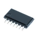
| 产品图片 |
|
| rohs | 符合RoHS无铅 / 符合限制有害物质指令(RoHS)规范要求 |
| 产品系列 | 逻辑集成电路,计数器移位寄存器,Texas Instruments SN74LV164ANSR74LV |
| 数据手册 | |
| 产品型号 | SN74LV164ANSR |
| 产品目录页面 | |
| 产品种类 | 计数器移位寄存器 |
| 传播延迟时间 | 21.1 ns, 16.3 ns, 11 ns |
| 供应商器件封装 | 14-SO |
| 元件数 | 1 |
| 其它名称 | 296-13228-6 |
| 功能 | 串行至并行 |
| 包装 | Digi-Reel® |
| 单位重量 | 210 mg |
| 商标 | Texas Instruments |
| 安装类型 | 表面贴装 |
| 安装风格 | SMD/SMT |
| 封装 | Reel |
| 封装/外壳 | 14-SOIC(0.209",5.30mm 宽) |
| 封装/箱体 | SOP-14 |
| 工作温度 | -40°C ~ 85°C |
| 工作电源电压 | 2.5 V, 3.3 V, 5 V |
| 工厂包装数量 | 2000 |
| 最大工作温度 | + 85 C |
| 最小工作温度 | - 40 C |
| 标准包装 | 1 |
| 每元件位数 | 8 |
| 电压-电源 | 2 V ~ 5.5 V |
| 电源电压-最大 | 5.5 V |
| 电源电压-最小 | 2 V |
| 电路数量 | 1 |
| 系列 | SN74LV164A |
| 计数顺序 | Serial to Parallel |
| 输入线路数量 | 2 |
| 输出类型 | 推挽式 |
| 输出线路数量 | 8 |
| 逻辑类型 | 移位寄存器 |
| 逻辑系列 | LV |


- 商务部:美国ITC正式对集成电路等产品启动337调查
- 曝三星4nm工艺存在良率问题 高通将骁龙8 Gen1或转产台积电
- 太阳诱电将投资9.5亿元在常州建新厂生产MLCC 预计2023年完工
- 英特尔发布欧洲新工厂建设计划 深化IDM 2.0 战略
- 台积电先进制程称霸业界 有大客户加持明年业绩稳了
- 达到5530亿美元!SIA预计今年全球半导体销售额将创下新高
- 英特尔拟将自动驾驶子公司Mobileye上市 估值或超500亿美元
- 三星加码芯片和SET,合并消费电子和移动部门,撤换高东真等 CEO
- 三星电子宣布重大人事变动 还合并消费电子和移动部门
- 海关总署:前11个月进口集成电路产品价值2.52万亿元 增长14.8%


PDF Datasheet 数据手册内容提取
Product Sample & Technical Tools & Support & Folder Buy Documents Software Community SN54LV164A,SN74LV164A SCLS403I–APRIL1998–REVISEDMARCH2015 SNx4LV164A 8-Bit Parallel-Out Serial Shift Registers 1 Features 2 Applications • 2-Vto5.5-VV Operation • IPRouters 1 CC • Maximumt of10.5nsat5V • EnterpriseSwitches pd • TypicalV (OutputGroundBounce) • AccessControlandSecurity:AccessKeypads OLP <0.8VatV =3.3V,T =25°C andBiometrics CC A • TypicalV (OutputV Undershoot) • SmartMeters:PowerLineCommunication OHV OH >2.3VatV =3.3V,T =25°C CC A 3 Description • IoffSupportsLiveInsertion,PartialPower-Down Mode,andBack-DriveProtection The SNx4LV164A devices are 8-bit parallel-out serial shift registers designed for 2-V to 5.5-V V • SupportMixed-ModeVoltageOperationon CC operation. AllPorts • Latch-upPerformanceExceeds250mA DeviceInformation(1) PerJESD17 PARTNUMBER PACKAGE BODYSIZE(NOM) • ESDProtectionExceedsJESD22 SOIC(14) 8.65mm×3.91mm – 2000-VHuman-BodyModel(A114-A) SSOP(14) 6.20mm×5.30mm – 1000-VCharged-DeviceModel(C101) TVSOP(14) 3.60mm×4.40mm SN74LV164A SOP(14) 10.30mm×5.30mm TSSOP(14) 5.00mm×4.40mm VQFN(14) 3.50mm×3.50mm (1) For all available packages, see the orderable addendum at theendofthedatasheet. LogicDiagram(PositiveLogic) 8 CLK 1 C1 C1 C1 C1 C1 C1 C1 C1 A 1D 1D 1D 1D 1D 1D 1D 1D 2 B R R R R R R R R 9 CLR 3 4 5 6 10 11 12 13 Q Q Q Q Q Q Q Q A B C D E F G H Pinnumbers shown are for the D, DB, DGV, J, NS, PW, RGY, and W packages. 1 An IMPORTANT NOTICE at the end of this data sheet addresses availability, warranty, changes, use in safety-critical applications, intellectualpropertymattersandotherimportantdisclaimers.UNLESSOTHERWISENOTED,thisdocumentcontainsPRODUCTION DATA.
SN54LV164A,SN74LV164A SCLS403I–APRIL1998–REVISEDMARCH2015 www.ti.com Table of Contents 1 Features.................................................................. 1 7 ParameterMeasurementInformation................10 2 Applications........................................................... 1 8 DetailedDescription............................................ 11 3 Description............................................................. 1 8.1 Overview.................................................................11 4 RevisionHistory..................................................... 2 8.2 FunctionalBlockDiagram.......................................11 5 PinConfigurationandFunctions......................... 3 8.3 FeatureDescription.................................................11 8.4 DeviceFunctionalModes........................................11 6 Specifications......................................................... 4 9 ApplicationandImplementation........................ 12 6.1 AbsoluteMaximumRatings......................................4 6.2 ESDRatings..............................................................4 9.1 ApplicationInformation............................................12 6.3 RecommendedOperatingConditions.......................5 9.2 TypicalApplication .................................................12 6.4 ThermalInformation..................................................5 10 PowerSupplyRecommendations..................... 14 6.5 ElectricalCharacteristics...........................................6 11 Layout................................................................... 14 6.6 TimingRequirements:V =2.5V±0.2V..............6 11.1 LayoutGuidelines.................................................14 CC 6.7 TimingRequirements:V =3.3V±0.3V..............6 11.2 LayoutExample....................................................14 CC 6.8 TimingRequirements:V =5V±0.5V.................7 12 DeviceandDocumentationSupport................. 15 CC 6.9 SwitchingCharacteristics:V =2.5V±0.2V........7 12.1 Trademarks...........................................................15 CC 6.10 SwitchingCharacteristics:V =3.3V±0.3V......7 12.2 ElectrostaticDischargeCaution............................15 CC 6.11 SwitchingCharacteristics:V =5V±0.5V.........8 12.3 Glossary................................................................15 CC 6.12 NoiseCharacteristics..............................................8 13 Mechanical,Packaging,andOrderable 6.13 OperatingCharacteristics........................................8 Information........................................................... 15 6.14 TypicalCharacteristics............................................9 4 Revision History ChangesfromRevisionH(April2005)toRevisionI Page • AddedPinConfigurationandFunctionssection,ESDRatingstable,FeatureDescriptionsection,DeviceFunctional Modes,ApplicationandImplementationsection,PowerSupplyRecommendationssection,Layoutsection,Device andDocumentationSupportsection,andMechanical,Packaging,andOrderableInformationsection .............................. 1 2 SubmitDocumentationFeedback Copyright©1998–2015,TexasInstrumentsIncorporated SN74LV164A
SN54LV164A,SN74LV164A www.ti.com SCLS403I–APRIL1998–REVISEDMARCH2015 5 Pin Configuration and Functions D,DB,DGV,NS,orPWPackage 14-PINSOIC,SSOP,TVSOP,SOP,orTSSOP RGYPackage TopView 14-PINVQFN TopView A 1 14 VCC CC A V B 2 13 Q H 1 14 Q 3 12 Q A G Q 4 11 Q B 2 13 QH B F Q 5 10 Q QA 3 12 QG C E Q 6 9 CLR QB 4 11 QF D Q 5 10 Q GND 7 8 CLK C E Q 6 9 CLR D 7 8 D K N L G C PinFunctions PIN I/O DESCRIPTION NO. NAME 1 A I SerialinputA 2 B I SerialinputB 3 Q O OutputA A 4 Q O OutputB B 5 Q O OutputC C 6 Q O OutputD D 7 GND – Groundpin 8 CLK I Storageclock 9 CLR I Storageclear 10 Q O OutputE E 11 Q O OutputF F 12 Q O OutputG G 13 Q O OutputH H 11 Q O Q inverted H' H 14 V – Powerpin CC Copyright©1998–2015,TexasInstrumentsIncorporated SubmitDocumentationFeedback 3 SN74LV164A
SN54LV164A,SN74LV164A SCLS403I–APRIL1998–REVISEDMARCH2015 www.ti.com 6 Specifications 6.1 Absolute Maximum Ratings(1) overoperatingfree-airtemperaturerange(unlessotherwisenoted) MIN MAX UNIT V Supplyvoltage –0.5 7 V CC V Inputvoltage(2) –0.5 7 V I V Voltageappliedtoanyoutputinthehigh-impedanceorpower-offstate(2) –0.5 7 V O V Outputvoltage(2)(3) –0.5 V +0.5 V O CC I Inputclampcurrent V <0 –20 mA IK I I Outputclampcurrent V <0 –50 mA OK O I Continuousoutputcurrent V =0toV ±25 mA O O CC ContinuouscurrentthroughV orGND ±50 mA CC T Storagetemperature –65 150 °C stg (1) StressesbeyondthoselistedunderAbsoluteMaximumRatingsmaycausepermanentdamagetothedevice.Thesearestressratings only,whichdonotimplyfunctionaloperationofthedeviceattheseoranyotherconditionsbeyondthoseindicatedunderRecommended OperatingConditions.Exposuretoabsolute-maximum-ratedconditionsforextendedperiodsmayaffectdevicereliability. (2) Theinputandoutputnegative-voltageratingsmaybeexceedediftheinputandoutputcurrentratingsareobserved. (3) Thisvalueislimitedto5.5Vmaximum. 6.2 ESD Ratings VALUE UNIT Humanbodymodel(HBM),perANSI/ESDA/JEDECJS-001(1) 2000 V(ESD) Electrostaticdischarge Charged-devicemodel(CDM),perJEDECspecificationJESD22- 1000 V C101(2) (1) JEDECdocumentJEP155statesthat500-VHBMallowssafemanufacturingwithastandardESDcontrolprocess. (2) JEDECdocumentJEP157statesthat250-VCDMallowssafemanufacturingwithastandardESDcontrolprocess. 4 SubmitDocumentationFeedback Copyright©1998–2015,TexasInstrumentsIncorporated SN74LV164A
SN54LV164A,SN74LV164A www.ti.com SCLS403I–APRIL1998–REVISEDMARCH2015 6.3 Recommended Operating Conditions overrecommendedoperatingfree-airtemperaturerange(unlessotherwisenoted)(1) SN54LV164A(2) SN74LV164A UNIT MIN MAX MIN MAX V Supplyvoltage 2 5.5 2 5.5 V CC V =2V 1.5 1.5 CC V =2.3Vto2.7V V ×0.7 V ×0.7 CC CC CC V High-levelinputvoltage V IH V =3Vto3.6V V ×0.7 V ×0.7 CC CC CC V =4.5Vto5.5V V ×0.7 V ×0.7 CC CC CC V =2V 0.5 0.5 CC V =2.3Vto2.7V V ×0.3 V ×0.3 CC CC CC V Low-levelinputvoltage V IL V =3Vto3.6V V ×0.3 V ×0.3 CC CC CC V =4.5Vto5.5V V ×0.3 V ×0.3 CC CC CC V Inputvoltage 0 5.5 0 5.5 V I V Outputvoltage 0 V 0 V V O CC CC V =2V –50 –50 µA CC V =2.3Vto2.7V –2 –2 CC I High-leveloutputcurrent OH V =3Vto3.6V –6 –6 mA CC V =4.5Vto5.5V –12 –12 CC V =2V 50 50 µA CC V =2.3Vto2.7V 2 2 CC I Low-leveloutputcurrent OL V =3Vto3.6V 6 6 mA CC V =4.5Vto5.5V 12 12 CC V =2.3Vto2.7V 200 200 CC Δt/Δv Inputtransitionriseorfallrate V =3Vto3.6V 100 100 ns/V CC V =4.5Vto5.5V 20 20 CC T Operatingfree-airtemperature –55 125 –40 125 °C A (1) AllunusedinputsofthedevicemustbeheldatV orGNDtoensureproperdeviceoperation.RefertotheTIapplicationreport, CC ImplicationsofSloworFloatingCMOSInputs,literaturenumberSCBA004. (2) ProductPreview 6.4 Thermal Information SN74LV164A THERMALMETRIC(1) D(SOIC) DB(SSOP) DGV NS(SOP) PW(TSSOP) RGY UNIT (TVSOP) (VQFN) 14PINS 14PINS 14PINS 14PINS 14PINS 14PINS RθJA Junction-to-ambientthermalresistance 92.6 104.4 126.7 89.3 120.2 54.5 RθJC(top) Junction-to-case(top)thermalresistance 53.9 57 50 46.9 48.9 67 RθJB Junction-to-boardthermalresistance 46.8 51.7 59.6 48 61.9 30.5 °C/W ψJT Junction-to-topcharacterizationparameter 18.9 18.6 5.8 13.7 5.7 2.3 ψJB Junction-to-boardcharacterizationparameter 46.6 51.2 58.9 47.7 61.3 30.5 RθJC(bot) Junction-to-case(bottom)thermalresistance – – – – – 11.2 (1) Formoreinformationabouttraditionalandnewthermalmetrics,seetheICPackageThermalMetricsapplicationreport,SPRA953. Copyright©1998–2015,TexasInstrumentsIncorporated SubmitDocumentationFeedback 5 SN74LV164A
SN54LV164A,SN74LV164A SCLS403I–APRIL1998–REVISEDMARCH2015 www.ti.com 6.5 Electrical Characteristics overrecommendedoperatingfree-airtemperaturerange(unlessotherwisenoted) SN54LV164A(1) SN74LV164A SN74LV164A PARAMTER TESTCONDITIONS VCC –40°Cto85°C –40°Cto125°C UNIT MIN TYP MAX MIN TYP MAX MIN TYP MAX 2Vto IOH=–50µA 5.5V VCC–0.1 VCC–0.1 VCC–0.1 VOH IOH=–2mA 2.3V 2 2 2 V IOH=–6mA 3V 2.48 2.48 2.48 IOH=–12mA 4.5V 3.8 3.8 3.8 2Vto IOL=50µA 5.5V 0.1 0.1 0.1 VOL IOL=2mA 2.3V 0.4 0.4 0.4 V IOL=6mA 3V 0.44 0.44 0.44 IOL=12mA 4.5V 0.55 0.55 0.55 0to II VI=5.5VorGND 5.5V ±1 ±1 ±1 µA ICC VI=VCCorGND, IO=0 5.5 20 20 20 µA Ioff VIorVO=0to5.5V 0 5 5 5 µA Ci VI=VCCorGND 3.3V 2.2 2.2 2.2 pF (1) ProductPreview 6.6 Timing Requirements: V = 2.5 V ± 0.2 V CC overrecommendedoperatingfree-airtemperaturerange,V =2.5V±0.2V(unlessotherwisenoted)(seeFigure4) CC TA=25°C SN54LV164A(1) –S4N07°C4LtVo18654°AC –S40N°7C4LtoV116245A°C UNIT MIN MAX MIN MAX MIN MAX MIN MAX CLRlow 6 6.5 6.5 6.5 tw Pulseduration ns CLKhighorlow 6.5 7.5 7.5 7.5 DatabeforeCLK↑ 6.5 8.5 8.5 8.5 tsu Setuptime ns CLRinactive 3 3 3 3 th Holdtime DataafterCLK↑ –0.5 0 0 0 ns (1) ProductPreview 6.7 Timing Requirements: V = 3.3 V ± 0.3 V CC overrecommendedoperatingfree-airtemperaturerange,V =3.3V±0.3V(unlessotherwisenoted)(seeFigure4) CC TA=25°C SN54LV164A(1) –S4N07°C4LtVo18654°AC –S40N°7C4LtoV116245A°C UNIT MIN MAX MIN MAX MIN MAX MIN MAX CLRlow 5 5 5 5 tw Pulseduration ns CLKhighorlow 5 5 5 5 DatabeforeCLK↑ 5 6 6 6 tsu Setuptime ns CLRinactive 2.5 2.5 2.5 2.5 th Holdtime DataafterCLK↑ 0 0 0 0 ns (1) ProductPreview 6 SubmitDocumentationFeedback Copyright©1998–2015,TexasInstrumentsIncorporated SN74LV164A
SN54LV164A,SN74LV164A www.ti.com SCLS403I–APRIL1998–REVISEDMARCH2015 6.8 Timing Requirements: V = 5 V ± 0.5 V CC overrecommendedoperatingfree-airtemperaturerange,V =5V±0.5V(unlessotherwisenoted)(seeFigure4) CC TA=25°C SN54LV164A(1) –S4N07°C4LtVo18654°AC –S40N°7C4LtoV116245A°C UNIT MIN MAX MIN MAX MIN MAX MIN MAX CLRlow 5 5 5 5 tw Pulseduration ns CLKhighorlow 5 5 5 5 DatabeforeCLK↑ 4.5 4.5 4.5 4.5 tsu Setuptime ns CLRinactive 2.5 2.5 2.5 2.5 th Holdtime DataafterCLK↑ 1 1 1 1 ns (1) ProductPreview 6.9 Switching Characteristics: V = 2.5 V ± 0.2 V CC overrecommendedoperatingfree-airtemperaturerange,V =2.5V±0.2V(unlessotherwisenoted)(seeFigure4) CC SN54LV164A SN74LV164A SN74LV164A PARAMETER FROM TO LOAD TA=25°C (1) –40°Cto85°C –40°Cto125°C UNIT (INPUT) (OUTPUT) CAPACITANCE MIN TYP MAX MIN MAX MIN MAX MIN MAX CL=15pF 55(2) 105(2) 50(2) 50 50 fmax MHz CL=50pF 45 85 40 40 40 tpd CLK Q 9.2(2) 17.6(2) 1(2) 20(2) 1 20 1 21 tPHL CLR Q CL=15pF 8.6(2) 16(2) 1(2) 18(2) 1 18 1 18.5 ns tpd CLK Q 11.5 21.1 1 24 1 24 1 25 CL=50pF ns tPHL CLR Q 10.8 19.5 1 22 1 22 1 22.5 (1) ProductPreview (2) OnproductscomplianttoMIL-PRF-38535,thisparameterisnotproductiontested. 6.10 Switching Characteristics: V = 3.3 V ± 0.3 V CC overrecommendedoperatingfree-airtemperaturerange,V =3.3V±0.3V(unlessotherwisenoted)(seeFigure4) CC SN54LV164A SN74LV164A SN74LV164A PARAMETER FROM TO LOAD TA=25°C (1) –40°Cto85°C –40°Cto125°C UNIT (INPUT) (OUTPUT) CAPACITANCE MIN TYP MAX MIN MAX MIN MAX MIN MAX CL=15pF 80(2) 155(2) 65(2) 65 65 fmax MHz CL=50pF 50 120 45 45 45 tpd CLK Q 6.4(2) 12.8(2) 1(2) 15(2) 1 15 1 16 tPHL CLR Q CL=15pF 6(2) 12.8(2) 1(2) 15(2) 1 15 1 16 ns tpd CLK Q 8.3 16.3 1 18.5 1 18.5 1 19.5 CL=50pF ns tPHL CLR Q 7.9 16.3 1 18.5 1 18.5 1 19.5 (1) ProductPreview (2) OnproductscomplianttoMIL-PRF-38535,thisparameterisnotproductiontested. Copyright©1998–2015,TexasInstrumentsIncorporated SubmitDocumentationFeedback 7 SN74LV164A
SN54LV164A,SN74LV164A SCLS403I–APRIL1998–REVISEDMARCH2015 www.ti.com 6.11 Switching Characteristics: V = 5 V ± 0.5 V CC overrecommendedoperatingfree-airtemperaturerange,V =5V±0.5V(unlessotherwisenoted)(seeFigure4) CC SN54LV164A SN74LV164A SN74LV164A PARAMETER FROM TO LOAD TA=25°C (1) –40°Cto85°C –40°Cto125°C UNIT (INPUT) (OUTPUT) CAPACITANCE MIN TYP MAX MIN MAX MIN MAX MIN MAX CL=15pF 125(2) 220(2) 105(2) 105 95 fmax MHz CL=50pF 85 165 75 75 65 tpd CLK Q 4.5(2) 9(2) 1(2) 10.5(2) 1 10.5 1 11.5 CL=15pF ns tPHL CLR Q 4.2(2) 8.6(2) 1(2) 10(2) 1 10 1 11 tpd CLK Q 6 11 1 12.5 1 12.5 1 13 CL=50pF ns tPHL CLR Q 5.8 10.6 1 12.5 1 12.5 1 13 (1) ProductPreview (2) OnproductscomplianttoMIL-PRF-38535,thisparameterisnotproductiontested. 6.12 Noise Characteristics(1) V =3.3V,C =50pF,T =25°C CC L A SN74LV164A PARAMETER UNIT MIN TYP MAX V Quietoutput,maximumdynamicV 0.28 0.8 V OL(P) OL V Quietoutput,minimumdynamicV –0.22 –0.8 V OL(V) OL V Quietoutput,minimumdynamicV 3.09 V OH(V) OH V High-leveldynamicinputvoltage 2.31 V IH(D) V Low-leveldynamicinputvoltage 0.99 V IL(D) (1) Characteristicsareforsurface-mountpackagesonly. 6.13 Operating Characteristics T =25°C A PARAMETER TESTCONDITIONS V TYP UNIT CC 3.3V 48.1 C Powerdissipationcapacitance C =50pF, f=10MHz pF pd L 5V 47.5 8 SubmitDocumentationFeedback Copyright©1998–2015,TexasInstrumentsIncorporated SN74LV164A
SN54LV164A,SN74LV164A www.ti.com SCLS403I–APRIL1998–REVISEDMARCH2015 CLR s put A n al I ri B e S CLK QA QB QC s QD ut p Out QE QF QG QH Clear Clear Figure1. TypicalClear,Shift,andClearSequences 6.14 Typical Characteristics 7 10 9 6 8 5 7 s) 4 s) 6 n n D ( D ( 5 P 3 P T T 4 2 3 2 1 1 0 0 -100 -50 0 50 100 150 0 1 2 3 4 5 6 Temperature Vcc D001 D002 Figure2.TPDvs.Temperatureat3.3V Figure3.TPDvs.V at25°C CC Copyright©1998–2015,TexasInstrumentsIncorporated SubmitDocumentationFeedback 9 SN74LV164A
SN54LV164A,SN74LV164A SCLS403I–APRIL1998–REVISEDMARCH2015 www.ti.com 7 Parameter Measurement Information VCC From Output Test From Output RL= 1 kΩ S1 Open TEST S1 UnderTest Point UnderTest GND tPLH/tPHL Open CL CL tPLZ/tPZL VCC (see NoteA) (see NoteA) tPHZ/tPZH GND Open Drain VCC LOAD CIRCUIT FOR LOAD CIRCUIT FOR TOTEM-POLE OUTPUTS 3-STATEAND OPEN-DRAIN OUTPUTS VCC Timing Input 50% VCC tw 0 V th VCC tsu VCC Input 50% VCC 50% VCC Data Input 50% VCC 50% VCC 0 V 0 V VOLTAGEWAVEFORMS VOLTAGEWAVEFORMS PULSEDURATION SETUPAND HOLD TIMES VCC Output VCC Input 50% VCC 50% VCC Control 50% VCC 50% VCC 0 V 0 V tPLH tPHL tPZL tPLZ VOH Output ≈VCC InO-Puhtapsuet 50%VCC 50% VCVCOL WaSv1e faot rVmC C1 50% VCC VOL+0.3V VOL (see Note B) tPHL tPLH tPZH tPHZ Output Out-ofO-Puhtapsuet 50% VCC 50% VCVVCOOHL (WseSae1v eNaftoo GtremN B D2) 50% VCC VOH−0.3VV≈0O HV VOLTAGEWAVEFORMS VOLTAGEWAVEFORMS PROPAGATIONDELAYTIMES ENABLEAND DISABLE TIMES INVERTINGAND NONINVERTING OUTPUTS LOW-AND HIGH-LEVELENABLING NOTES: A. CLincludes probe and jig capacitance. B. Waveform 1 is for an output with internal conditions such that the output is low, except when disabled by the output control. Waveform 2 is for an output with internal conditions such that the output is high, except when disabled by the output control. C. Allinputpulsesaresuppliedbygeneratorshavingthefollowingcharacteristics: PRR≤1 MHz, ZO= 50Ω, tr≤3ns,tf≤3 ns. D. Theoutputsaremeasuredoneatatime,withoneinputtransitionpermeasurement. E. tPLZandtPHZarethesameastdis. F. tPZLandtPZHarethesameasten. G. tPHLandtPLHare the same as tpd. H. Allparametersandwaveformsarenotapplicabletoalldevices. Figure4. LoadCircuitandVoltageWaveforms 10 SubmitDocumentationFeedback Copyright©1998–2015,TexasInstrumentsIncorporated SN74LV164A
SN54LV164A,SN74LV164A www.ti.com SCLS403I–APRIL1998–REVISEDMARCH2015 8 Detailed Description 8.1 Overview TheSNx4LV164Adevicesare8-bitparallel-outserialshiftregistersdesignedfor2-Vto5.5-VV operation. CC These devices feature NAND-gated serial (A and B) inputs and an asynchronous clear (CLR) input. The gated serial inputs permit complete control over incoming data, as a low at either input inhibits entry of the new data and resets the first flip-flop to the low level at the next clock pulse. A high-level input enables the other input, which then determines the state of the first flip-flop. Data at the serial inputs can be changed while the clock is high or low, provided the minimum setup time requirements are met. Clocking occurs on the low-to-high-level transitionoftheclock(CLK)input. 8.2 Functional Block Diagram 8 CLK 1 C1 C1 C1 C1 C1 C1 C1 C1 A 1D 1D 1D 1D 1D 1D 1D 1D 2 B R R R R R R R R 9 CLR 3 4 5 6 10 11 12 13 Q Q Q Q Q Q Q Q A B C D E F G H Pinnumbers shown are for the D, DB, DGV, J, NS, PW, RGY, and W packages. Figure5. LogicDiagram(PositiveLogic) 8.3 Feature Description The wide operating range allows the device to be used in a variety of systems that use different logic levels. The low propagation delay allows fast switching and higher speeds of operation. In addition, the low ground bounce stabilizestheperformanceofnon-switchingoutputswhileanotheroutputisswitching. 8.4 Device Functional Modes Table1.FunctionTable(1)(2) INPUTS OUTPUTS CLR CLK A B Q Q ... Q A B H L X X X L L L H L X X Q Q Q A0 B0 H0 H ↑ H H H Q Q An Gn H ↑ L X L Q Q An Gn H ↑ X L L Q Q An Gn (1) Q ,Q ,Q =thelevelofQ ,Q ,orQ ,respectively,beforethe A0 B0 H0 A B H indicatedsteady-stateinputconditionswereestablished. (2) Q ,Q =thelevelofQ orQ beforethemostrecent↑transition An Gn A G oftheclock:indicatesa1-bitshift. Copyright©1998–2015,TexasInstrumentsIncorporated SubmitDocumentationFeedback 11 SN74LV164A
SN54LV164A,SN74LV164A SCLS403I–APRIL1998–REVISEDMARCH2015 www.ti.com 9 Application and Implementation NOTE Information in the following applications sections is not part of the TI component specification, and TI does not warrant its accuracy or completeness. TI’s customers are responsible for determining suitability of components for their purposes. Customers should validateandtesttheirdesignimplementationtoconfirmsystemfunctionality. 9.1 Application Information The SN74LV164A is a low drive CMOS device that can be used for a multitude of bus interface type applications where output ringing is a concern. The low-drive and slow-edge rates will minimize overshoot and undershoot on theoutputs. 9.2 Typical Application Figure6. TypicalApplicationSchematic 9.2.1 DesignRequirements ThisdeviceusesCMOStechnologyandhasbalancedoutputdrive.Takecaretoavoidbuscontentionbecauseit can drive currents that would exceed maximum limits. The high drive will also create fast edges into light loads soconsiderroutingandloadconditionstopreventringing. 9.2.2 DetailedDesignProcedure • Recommendedinputconditions: – Risetimeandfalltimespecs.See(Δt/ΔV)inRecommendedOperatingConditions. – Specifiedhighandlowlevel.See(V andV )inRecommendedOperatingConditions. IH IL – Inputsareovervoltagetolerantallowingthemtogoashighas5.5VatanyvalidV . CC • Recommendedoutputconditions: – Loadcurrentsshouldnotexceed25mAperoutputand50mAtotalforthepart. – OutputsshouldnotbepulledaboveV . CC 12 SubmitDocumentationFeedback Copyright©1998–2015,TexasInstrumentsIncorporated SN74LV164A
SN54LV164A,SN74LV164A www.ti.com SCLS403I–APRIL1998–REVISEDMARCH2015 Typical Application (continued) 9.2.3 ApplicationCurves Figure7. SwitchingCharacteristicsComparison Copyright©1998–2015,TexasInstrumentsIncorporated SubmitDocumentationFeedback 13 SN74LV164A
SN54LV164A,SN74LV164A SCLS403I–APRIL1998–REVISEDMARCH2015 www.ti.com 10 Power Supply Recommendations The power supply can be any voltage between the minimum and maximum supply voltage rating located in the Recommended Operating Conditions. Each V terminal should have a good bypass capacitor to prevent power CC disturbance. For devices with a single supply, TI recommends a 0.1-μF capacitor and if there are multiple V CC terminals then TI recommends a 0.01-μF or 0.022-μF capacitor for each power terminal. Multiple bypass capacitors can be paralleled to reject different frequencies of noise. Frequencies of 0.1 μF and 1 μF are commonly used in parallel. The bypass capacitor should be installed as close as possible to the power terminal forbestresults. 11 Layout 11.1 Layout Guidelines Whenusingmultiplebitlogicdevicesinputsshouldnoteverfloat. In many cases, functions or parts of functions of digital logic devices are unused, for example, when only two inputs of a triple-input AND gate are used or only three of the four buffer gates are used. Such input pins should not be left unconnected because the undefined voltages at the outside connections result in undefined operational states. Specified below are the rules that must be observed under all circumstances. All unused inputs of digital logic devices must be connected to a high or low bias to prevent them from floating. The logic level that should be applied to any particular unused input depends on the function of the device. Generally they will be tied to GND or V whichever make more sense or is more convenient. Floating outputs is generally CC acceptable, unless the part is a transceiver. If the transceiver has an output enable pin it will disable the outputs section of the part when asserted. This will not disable the input section of the I.O’s so they also cannot float whendisabled. 11.2 Layout Example Figure8. LayoutExample 14 SubmitDocumentationFeedback Copyright©1998–2015,TexasInstrumentsIncorporated SN74LV164A
SN54LV164A,SN74LV164A www.ti.com SCLS403I–APRIL1998–REVISEDMARCH2015 12 Device and Documentation Support 12.1 Trademarks Alltrademarksarethepropertyoftheirrespectiveowners. 12.2 Electrostatic Discharge Caution Thesedeviceshavelimitedbuilt-inESDprotection.Theleadsshouldbeshortedtogetherorthedeviceplacedinconductivefoam duringstorageorhandlingtopreventelectrostaticdamagetotheMOSgates. 12.3 Glossary SLYZ022—TIGlossary. Thisglossarylistsandexplainsterms,acronyms,anddefinitions. 13 Mechanical, Packaging, and Orderable Information The following pages include mechanical, packaging, and orderable information. This information is the most current data available for the designated devices. This data is subject to change without notice and revision of thisdocument.Forbrowser-basedversionsofthisdatasheet,refertotheleft-handnavigation. Copyright©1998–2015,TexasInstrumentsIncorporated SubmitDocumentationFeedback 15 SN74LV164A
PACKAGE OPTION ADDENDUM www.ti.com 24-Aug-2018 PACKAGING INFORMATION Orderable Device Status Package Type Package Pins Package Eco Plan Lead/Ball Finish MSL Peak Temp Op Temp (°C) Device Marking Samples (1) Drawing Qty (2) (6) (3) (4/5) SN74LV164AD ACTIVE SOIC D 14 50 Green (RoHS CU NIPDAU Level-1-260C-UNLIM -40 to 125 LV164A & no Sb/Br) SN74LV164ADBR ACTIVE SSOP DB 14 2000 Green (RoHS CU NIPDAU Level-1-260C-UNLIM -40 to 125 LV164A & no Sb/Br) SN74LV164ADGVR ACTIVE TVSOP DGV 14 2000 Green (RoHS CU NIPDAU Level-1-260C-UNLIM -40 to 125 LV164A & no Sb/Br) SN74LV164ADR ACTIVE SOIC D 14 2500 Green (RoHS CU NIPDAU Level-1-260C-UNLIM -40 to 125 LV164A & no Sb/Br) SN74LV164ANSR ACTIVE SO NS 14 2000 Green (RoHS CU NIPDAU Level-1-260C-UNLIM -40 to 125 74LV164A & no Sb/Br) SN74LV164APW ACTIVE TSSOP PW 14 90 Green (RoHS CU NIPDAU Level-1-260C-UNLIM -40 to 125 LV164A & no Sb/Br) SN74LV164APWG4 ACTIVE TSSOP PW 14 90 Green (RoHS CU NIPDAU Level-1-260C-UNLIM -40 to 125 LV164A & no Sb/Br) SN74LV164APWR ACTIVE TSSOP PW 14 2000 Green (RoHS CU NIPDAU Level-1-260C-UNLIM -40 to 125 LV164A & no Sb/Br) SN74LV164APWRG4 ACTIVE TSSOP PW 14 2000 Green (RoHS CU NIPDAU Level-1-260C-UNLIM -40 to 125 LV164A & no Sb/Br) SN74LV164APWT ACTIVE TSSOP PW 14 250 Green (RoHS CU NIPDAU Level-1-260C-UNLIM -40 to 125 LV164A & no Sb/Br) SN74LV164ARGYR ACTIVE VQFN RGY 14 3000 Green (RoHS CU NIPDAU Level-2-260C-1 YEAR -40 to 125 LV164A & no Sb/Br) (1) The marketing status values are defined as follows: ACTIVE: Product device recommended for new designs. LIFEBUY: TI has announced that the device will be discontinued, and a lifetime-buy period is in effect. NRND: Not recommended for new designs. Device is in production to support existing customers, but TI does not recommend using this part in a new design. PREVIEW: Device has been announced but is not in production. Samples may or may not be available. OBSOLETE: TI has discontinued the production of the device. (2) RoHS: TI defines "RoHS" to mean semiconductor products that are compliant with the current EU RoHS requirements for all 10 RoHS substances, including the requirement that RoHS substance do not exceed 0.1% by weight in homogeneous materials. Where designed to be soldered at high temperatures, "RoHS" products are suitable for use in specified lead-free processes. TI may reference these types of products as "Pb-Free". RoHS Exempt: TI defines "RoHS Exempt" to mean products that contain lead but are compliant with EU RoHS pursuant to a specific EU RoHS exemption. Green: TI defines "Green" to mean the content of Chlorine (Cl) and Bromine (Br) based flame retardants meet JS709B low halogen requirements of <=1000ppm threshold. Antimony trioxide based flame retardants must also meet the <=1000ppm threshold requirement. Addendum-Page 1
PACKAGE OPTION ADDENDUM www.ti.com 24-Aug-2018 (3) MSL, Peak Temp. - The Moisture Sensitivity Level rating according to the JEDEC industry standard classifications, and peak solder temperature. (4) There may be additional marking, which relates to the logo, the lot trace code information, or the environmental category on the device. (5) Multiple Device Markings will be inside parentheses. Only one Device Marking contained in parentheses and separated by a "~" will appear on a device. If a line is indented then it is a continuation of the previous line and the two combined represent the entire Device Marking for that device. (6) Lead/Ball Finish - Orderable Devices may have multiple material finish options. Finish options are separated by a vertical ruled line. Lead/Ball Finish values may wrap to two lines if the finish value exceeds the maximum column width. Important Information and Disclaimer:The information provided on this page represents TI's knowledge and belief as of the date that it is provided. TI bases its knowledge and belief on information provided by third parties, and makes no representation or warranty as to the accuracy of such information. Efforts are underway to better integrate information from third parties. TI has taken and continues to take reasonable steps to provide representative and accurate information but may not have conducted destructive testing or chemical analysis on incoming materials and chemicals. TI and TI suppliers consider certain information to be proprietary, and thus CAS numbers and other limited information may not be available for release. In no event shall TI's liability arising out of such information exceed the total purchase price of the TI part(s) at issue in this document sold by TI to Customer on an annual basis. Addendum-Page 2
PACKAGE MATERIALS INFORMATION www.ti.com 20-Dec-2018 TAPE AND REEL INFORMATION *Alldimensionsarenominal Device Package Package Pins SPQ Reel Reel A0 B0 K0 P1 W Pin1 Type Drawing Diameter Width (mm) (mm) (mm) (mm) (mm) Quadrant (mm) W1(mm) SN74LV164ADGVR TVSOP DGV 14 2000 330.0 12.4 6.8 4.0 1.6 8.0 12.0 Q1 SN74LV164ADR SOIC D 14 2500 330.0 16.4 6.5 9.0 2.1 8.0 16.0 Q1 SN74LV164ANSR SO NS 14 2000 330.0 16.4 8.2 10.5 2.5 12.0 16.0 Q1 SN74LV164APWR TSSOP PW 14 2000 330.0 12.4 6.9 5.6 1.6 8.0 12.0 Q1 SN74LV164APWT TSSOP PW 14 250 330.0 12.4 6.9 5.6 1.6 8.0 12.0 Q1 SN74LV164ARGYR VQFN RGY 14 3000 330.0 12.4 3.75 3.75 1.15 8.0 12.0 Q1 PackMaterials-Page1
PACKAGE MATERIALS INFORMATION www.ti.com 20-Dec-2018 *Alldimensionsarenominal Device PackageType PackageDrawing Pins SPQ Length(mm) Width(mm) Height(mm) SN74LV164ADGVR TVSOP DGV 14 2000 367.0 367.0 35.0 SN74LV164ADR SOIC D 14 2500 367.0 367.0 38.0 SN74LV164ANSR SO NS 14 2000 367.0 367.0 38.0 SN74LV164APWR TSSOP PW 14 2000 367.0 367.0 35.0 SN74LV164APWT TSSOP PW 14 250 367.0 367.0 35.0 SN74LV164ARGYR VQFN RGY 14 3000 367.0 367.0 35.0 PackMaterials-Page2
None
None
None
None
MECHANICAL DATA MPDS006C – FEBRUARY 1996 – REVISED AUGUST 2000 DGV (R-PDSO-G**) PLASTIC SMALL-OUTLINE 24 PINS SHOWN 0,23 0,40 0,07 M 0,13 24 13 0,16 NOM 4,50 6,60 4,30 6,20 Gage Plane 0,25 0°–(cid:1)8° 0,75 1 12 0,50 A Seating Plane 0,15 1,20 MAX 0,08 0,05 PINS ** 14 16 20 24 38 48 56 DIM A MAX 3,70 3,70 5,10 5,10 7,90 9,80 11,40 A MIN 3,50 3,50 4,90 4,90 7,70 9,60 11,20 4073251/E 08/00 NOTES: A. All linear dimensions are in millimeters. B. This drawing is subject to change without notice. C. Body dimensions do not include mold flash or protrusion, not to exceed 0,15 per side. D. Falls within JEDEC: 24/48 Pins – MO-153 14/16/20/56 Pins – MO-194 • POST OFFICE BOX 655303 DALLAS, TEXAS 75265
MECHANICAL DATA MSSO002E – JANUARY 1995 – REVISED DECEMBER 2001 DB (R-PDSO-G**) PLASTIC SMALL-OUTLINE 28 PINS SHOWN 0,38 0,65 0,15 M 0,22 28 15 0,25 0,09 5,60 8,20 5,00 7,40 Gage Plane 1 14 0,25 A 0°–(cid:1)8° 0,95 0,55 Seating Plane 2,00 MAX 0,05 MIN 0,10 PINS ** 14 16 20 24 28 30 38 DIM A MAX 6,50 6,50 7,50 8,50 10,50 10,50 12,90 A MIN 5,90 5,90 6,90 7,90 9,90 9,90 12,30 4040065/E 12/01 NOTES: A. All linear dimensions are in millimeters. B. This drawing is subject to change without notice. C. Body dimensions do not include mold flash or protrusion not to exceed 0,15. D. Falls within JEDEC MO-150 • POST OFFICE BOX 655303 DALLAS, TEXAS 75265
None
None
None
None
IMPORTANTNOTICEANDDISCLAIMER TIPROVIDESTECHNICALANDRELIABILITYDATA(INCLUDINGDATASHEETS),DESIGNRESOURCES(INCLUDINGREFERENCE DESIGNS),APPLICATIONOROTHERDESIGNADVICE,WEBTOOLS,SAFETYINFORMATION,ANDOTHERRESOURCES“ASIS” ANDWITHALLFAULTS,ANDDISCLAIMSALLWARRANTIES,EXPRESSANDIMPLIED,INCLUDINGWITHOUTLIMITATIONANY IMPLIEDWARRANTIESOFMERCHANTABILITY,FITNESSFORAPARTICULARPURPOSEORNON-INFRINGEMENTOFTHIRD PARTYINTELLECTUALPROPERTYRIGHTS. TheseresourcesareintendedforskilleddevelopersdesigningwithTIproducts.Youaresolelyresponsiblefor(1)selectingtheappropriate TIproductsforyourapplication,(2)designing,validatingandtestingyourapplication,and(3)ensuringyourapplicationmeetsapplicable standards,andanyothersafety,security,orotherrequirements.Theseresourcesaresubjecttochangewithoutnotice.TIgrantsyou permissiontousetheseresourcesonlyfordevelopmentofanapplicationthatusestheTIproductsdescribedintheresource.Other reproductionanddisplayoftheseresourcesisprohibited.NolicenseisgrantedtoanyotherTIintellectualpropertyrightortoanythird partyintellectualpropertyright.TIdisclaimsresponsibilityfor,andyouwillfullyindemnifyTIanditsrepresentativesagainst,anyclaims, damages,costs,losses,andliabilitiesarisingoutofyouruseoftheseresources. TI’sproductsareprovidedsubjecttoTI’sTermsofSale(www.ti.com/legal/termsofsale.html)orotherapplicabletermsavailableeitheron ti.comorprovidedinconjunctionwithsuchTIproducts.TI’sprovisionoftheseresourcesdoesnotexpandorotherwisealterTI’sapplicable warrantiesorwarrantydisclaimersforTIproducts. MailingAddress:TexasInstruments,PostOfficeBox655303,Dallas,Texas75265 Copyright©2019,TexasInstrumentsIncorporated