 Datasheet下载
- 型号: SN74LS273DWR
- 制造商: Texas Instruments
- 库位|库存: xxxx|xxxx
- 要求:
| 数量阶梯 | 香港交货 | 国内含税 |
| +xxxx | $xxxx | ¥xxxx |
查看当月历史价格
查看今年历史价格
SN74LS273DWR产品简介:
ICGOO电子元器件商城为您提供SN74LS273DWR由Texas Instruments设计生产,在icgoo商城现货销售,并且可以通过原厂、代理商等渠道进行代购。 SN74LS273DWR价格参考。Texas InstrumentsSN74LS273DWR封装/规格:逻辑 - 触发器, Flip Flop 1 Element D-Type 8 Bit Positive Edge 20-SOIC (0.295", 7.50mm Width)。您可以下载SN74LS273DWR参考资料、Datasheet数据手册功能说明书,资料中有SN74LS273DWR 详细功能的应用电路图电压和使用方法及教程。
SN74LS273DWR是德州仪器(Texas Instruments)生产的一款8位D型触发器集成电路,属于逻辑 - 触发器类别。该器件带有公共时钟和直接清零功能,采用双列直插式封装(SOIC),适用于需要同步数据存储和传输的数字系统。

主要应用场景包括:

1. 数据锁存与缓冲:在微处理器或微控制器系统中,用于锁存地址或数据信号,实现总线隔离与驱动,提升系统稳定性。

2. 时序控制电路:广泛应用于工业控制设备中,如PLC、计数器、定时器等,用于同步多个操作步骤,确保信号按预定时序执行。

3. 数字系统接口:在通信接口电路中,作为并行数据的暂存单元,协调高速处理器与低速外设之间的数据交换。

4. LED显示驱动:常用于多位数码管或LED点阵显示屏的驱动电路中,通过锁存数据稳定输出,避免显示闪烁。

5. 状态寄存器:在嵌入式系统中用作状态或控制寄存器,保存系统运行过程中的关键状态信息。

SN74LS273DWR基于传统的LS(Low-power Schottky)TTL技术,具备较高的抗干扰能力和稳定的工作性能,适合工业环境下的中低速数字设计。虽然功耗略高于现代CMOS器件,但其可靠性和成熟的设计支持使其仍在教育实验、工业升级和维修替换中广泛应用。
| 参数 | 数值 |
| 产品目录 | 集成电路 (IC)半导体 |
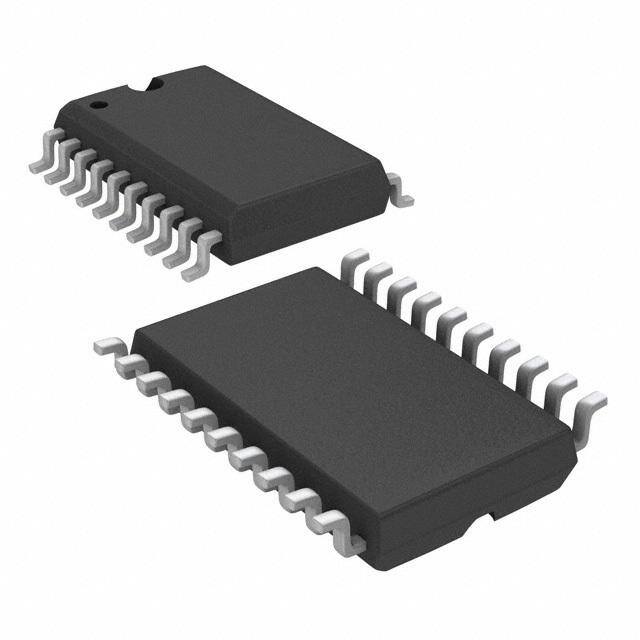
| 描述 | IC D-TYPE POS TRG SNGL 20SOIC触发器 Octal D-Type Flip-Flop w/Clear |
| 产品分类 | |
| 品牌 | Texas Instruments |
| 产品手册 | |
| 产品图片 |
|
| rohs | 符合RoHS无铅 / 符合限制有害物质指令(RoHS)规范要求 |
| 产品系列 | 逻辑集成电路,触发器,Texas Instruments SN74LS273DWR74LS |
| 数据手册 | |
| 产品型号 | SN74LS273DWR |
| 不同V、最大CL时的最大传播延迟 | 27ns @ 5V,15pF |
| 产品目录页面 | |
| 产品种类 | 触发器 |
| 传播延迟时间 | 27 ns |
| 低电平输出电流 | 8 mA |
| 元件数 | 1 |
| 其它名称 | 296-3682-1 |
| 功能 | 主复位 |
| 包装 | 剪切带 (CT) |
| 单位重量 | 500.700 mg |
| 商标 | Texas Instruments |
| 安装类型 | 表面贴装 |
| 安装风格 | SMD/SMT |
| 封装 | Reel |
| 封装/外壳 | 20-SOIC(0.295",7.50mm 宽) |
| 封装/箱体 | SOIC-20 Wide |
| 工作温度 | 0°C ~ 70°C |
| 工厂包装数量 | 2000 |
| 最大工作温度 | + 70 C |
| 最小工作温度 | 0 C |
| 极性 | Non-Inverting |
| 标准包装 | 1 |
| 每元件位数 | 8 |
| 电压-电源 | 4.75 V ~ 5.25 V |
| 电流-输出高,低 | 400µA, 8mA |
| 电流-静态 | 27mA |
| 电源电压-最大 | 5.25 V |
| 电源电压-最小 | 4.75 V |
| 电路数量 | 8 |
| 类型 | D 型 |
| 系列 | SN74LS273 |
| 触发器类型 | 正边沿 |
| 输入电容 | - |
| 输入类型 | TTL |
| 输入线路数量 | 2 |
| 输出类型 | 非反相 |
| 输出线路数量 | 1 |
| 逻辑类型 | D-Type Flip-Flop |
| 逻辑系列 | LS |
| 频率-时钟 | 40MHz |
| 高电平输出电流 | - 0.4 mA |


- 商务部:美国ITC正式对集成电路等产品启动337调查
- 曝三星4nm工艺存在良率问题 高通将骁龙8 Gen1或转产台积电
- 太阳诱电将投资9.5亿元在常州建新厂生产MLCC 预计2023年完工
- 英特尔发布欧洲新工厂建设计划 深化IDM 2.0 战略
- 台积电先进制程称霸业界 有大客户加持明年业绩稳了
- 达到5530亿美元!SIA预计今年全球半导体销售额将创下新高
- 英特尔拟将自动驾驶子公司Mobileye上市 估值或超500亿美元
- 三星加码芯片和SET,合并消费电子和移动部门,撤换高东真等 CEO
- 三星电子宣布重大人事变动 还合并消费电子和移动部门
- 海关总署:前11个月进口集成电路产品价值2.52万亿元 增长14.8%


PDF Datasheet 数据手册内容提取
SN54273, SN54LS273, SN74273, SN74LS273 OCTAL D-TYPE FLIP-FLOP WITH CLEAR SDLS090 – OCTOBER 1976 – REVISED MARCH 1988 • Contains Eight Flip-Flops With Single-Rail SN54273, SN74LS273...J OR W PACKAGE Outputs SN74273...N PACKAGE • SN74LS273...DW OR N PACKAGE Buffered Clock and Direct Clear Inputs (TOP VIEW) • Individual Data Input to Each Flip-Flop • Applications Include: CLR 1 20 VCC Buffer/Storage Registers 1Q 2 19 8Q Shift Registers 1D 3 18 8D Pattern Generators 2D 4 17 7D 2Q 5 16 7Q description 3Q 6 15 6Q 3D 7 14 6D These monolithic, positive-edge-triggered flip- 4D 8 13 5D flops utilize TTL circuitry to implement D-type 4Q 9 12 5Q flip-flop logic with a direct clear input. GND 10 11 CLK Information at the D inputs meeting the setup time requirements is transferred to the Q outputs on the positive-going edge of the clock pulse. Clock SN54LS273...FK PACKAGE (TOP VIEW) triggering occurs at a particular voltage level and is not directly related to the transition time of the C R C positive-going pulse. When the clock input is at D Q L Q 1 1 CV 8 either the high or low level, the D input signal has no effect ar the output. 3 2 1 20 19 2D 4 18 8D These flip-flops are guaranteed to respond to 2Q 5 17 7D clock frequencies ranging form 0 to 30 megahertz 3Q 6 16 7Q while maximum clock frequency is typically 40 3D 7 15 6Q megahertz. Typical power dissipation is 39 4D 8 14 6D milliwatts per flip-flop for the ′273 and 10 milliwatts 9 10 11 12 13 for the ′LS273. Q D KQ D 4 N L5 5 G C FUNCTION TABLE logic symbol† (each flip-flop) INPUTS OUTPUT 1 CLR EN CLEAR CLOCK D Q 11 CLK C1 L X X L H ↑ H H 3 2 1D 1D 1Q H ↑ L L 4 5 2D 2Q 7 6 H L X Q0 3D 3Q 8 9 4D 4Q 13 12 5D 5Q 14 15 6D 6Q 17 16 7D 7Q 18 19 8D 8Q †This symbol is in accordance with ANSI/IEEE Std. 91-1984 and IEC Publication 617-12. Pin numbers shown are for the DW, J, N, and W packages. PRODUCTION DATA information is current as of publication date. Copyright 1988, Texas Instruments Incorporated Products conform to specifications per the terms of Texas Instruments standard warranty. Production processing does not necessarily include testing of all parameters. POST OFFICE BOX 655303 • DALLAS, TEXAS 75265 1
SN54273, SN54LS273, SN74273, SN74LS273 OCTAL D-TYPE FLIP-FLOP WITH CLEAR SDLS090 – OCTOBER 1976 – REVISED MARCH 1988 schematics of inputs and outputs ′273 EQUIVALENT OF EACH INPUT TYPICAL OF ALL OUTPUTS VCC VCC Req 100 W NOM INPUT OUTPUT Clear: Req = 3 kW NOM Clock: Req = 6 kW NOM All other inputs: Req = 8 kW NOM ′LS273 EQUIVALENT OF EACH INPUT TYPICAL OF ALL OUTPUTS VCC 120 W NOM VCC 20 kW NOM INPUT OUTPUT logic diagram (positive logic) 1D 2D 3D 4D 5D 6D 7D 8D 11 3 4 7 8 13 14 17 18 CLOCK 1D 1D 1D 1D 1D 1D 1D 1D C1 C1 C1 C1 C1 C1 C1 C1 R R R R R R R R 1 CLEAR 2 5 6 9 12 15 16 19 1Q 2Q 3Q 4Q 5Q 6Q 7Q 8Q Pin numbers shown are for the DW, J, N, and W packages. 2 POST OFFICE BOX 655303 • DALLAS, TEXAS 75265
SN54273, SN54LS273, SN74273, SN74LS273 OCTAL D-TYPE FLIP-FLOP WITH CLEAR SDLS090 – OCTOBER 1976 – REVISED MARCH 1988 absolute maximum ratings over operating free-air temperature range (unless otherwise noted) Supply voltage, VCC (see Note 1) . . . . . . . . . . . . . . . . . . . . . . . . . . . . . . . . . . . . . . . . . . . . . . . . . . . . . . . . . . . . 7 V Input voltage . . . . . . . . . . . . . . . . . . . . . . . . . . . . . . . . . . . . . . . . . . . . . . . . . . . . . . . . . . . . . . . . . . . . . . . . . . . 5.5 V Operating free-air temperature range, T : SN54273 . . . . . . . . . . . . . . . . . . . . . . . . . . . . . . . . . –55°C to 125°C A SN74273 . . . . . . . . . . . . . . . . . . . . . . . . . . . . . . . . . . . . 0°C to 70°C Storage temperature range . . . . . . . . . . . . . . . . . . . . . . . . . . . . . . . . . . . . . . . . . . . . . . . . . . . . . . . –65°C to 150°C NOTE 1: Voltage values are with respect to network ground terminal. recommended operating conditions SN54273 SN74273 UUNNIITT MIN NOM MAX MIN NOM MAX Supply voltage, VCC 4.5 5 5.5 4.75 5 5.25 V High-level output current, IOH –800 –800 m A Low-level output current, IOL 16 16 mA Clock frequency, fclock 0 30 0 30 MHz Width of clock or clear pulse, tw 16.5 16.5 ns Data input 20↑ 20↑ SSeettuupp ttiimmee, ttsu nnss Clear inactive state 25↑ 25↑ Data hold time, th 5↑ 5↑ ns Operating free-air temperature, TA –55 125 0 70 °C ↑The arrow indicates that the rising edge of the clock pulse is used for reference. electrical characteristics over recommended operating free-air temperature range (unless otherwise noted) PARAMETER TEST CONDITIONS† MIN TYP‡ MAX UNIT VIH High-level input voltage 2 V VIL Low-level input voltage 0.8 V VIK Input clamp voltage VCC = MIN, II = –12 mA –1.5 V VCC = MIN, VIH = 2 V, VOH High-level output voltage VIL = 0.8 V, IOH = –800 m A 2.4 3.4 V VCC = MIN, VIH = 2 V, VOL Low-level output voltage 0.4 V VIL = 0.8 V, IOH = 16 mA II Input current at maximum input voltage VCC = MAX, VI = 5.5 V 1 mA Clear 80 IIIIHH HHiigghh-lleevveell iinnppuutt ccuurrrreenntt VVCCCC == MMAAXX, VVII == 22.44 VV mm AA Clock or D 40 Clear –3.2 IIIILL LLooww-lleevveell iinnppuutt ccuurrrreenntt VVCCCC == MMAAXX, VVII == 00.44 VV mmAA Clock or D –1.6 IOS Short-circuit output current§ VCC = MAX –18 –57 mA ICC Supply current VCC = MAX, See Note 2 62 94 mA †For conditions shown as MIN or MAX, use the appropriate value specified under recommended operating conditions. ‡All typical values are at VCC = 5 V, TA = 25°C. §Not more than one output should be shorted at a time. NOTE 2: With all outputs open and 4.5 V applied to all data and clear inputs, ICC is measured after a momentary ground, then 4.5 V, is applied to clock. POST OFFICE BOX 655303 • DALLAS, TEXAS 75265 3
SN54273, SN54LS273, SN74273, SN74LS273 OCTAL D-TYPE FLIP-FLOP WITH CLEAR SDLS090 – OCTOBER 1976 – REVISED MARCH 1988 switching characteristics, V = 5 V, T = 25°C CC A PARAMETER TEST CONDITIONS MIN TYP MAX UNIT fmax Maximum clock frequency 30 40 MHz tPHL Propagation delay time, high-to-low-level output from clear CCRRLLL === 4140500 0p FWW ,, 18 27 ns tPLH Propagation delay time, low-to-high-level output from clock SSeeee NNoottee 33 17 27 ns tPHL Propagation delay time, high-to-low-level output from clock 18 27 ns NOTE 3: Load circuits and voltage waveforms are shown in Section 1. absolute maximum ratings over operating free-air temperature range (unless otherwise noted) Supply voltage, VCC (see Note 1) . . . . . . . . . . . . . . . . . . . . . . . . . . . . . . . . . . . . . . . . . . . . . . . . . . . . . . . . . . . . 7 V Input voltage . . . . . . . . . . . . . . . . . . . . . . . . . . . . . . . . . . . . . . . . . . . . . . . . . . . . . . . . . . . . . . . . . . . . . . . . . . . . . 7 V Operating free-air temperature range, T : SN54LS273 . . . . . . . . . . . . . . . . . . . . . . . . . . . . . . –55°C to 125°C A SN74LS273 . . . . . . . . . . . . . . . . . . . . . . . . . . . . . . . . . 0°C to 70°C Storage temperature range . . . . . . . . . . . . . . . . . . . . . . . . . . . . . . . . . . . . . . . . . . . . . . . . . . . . . . . –65°C to 150°C NOTE 1: Voltage values are with respect to network ground terminal. recommended operating conditions SN54LS273 SN74LS273 UUNNIITT MIN NOM MAX MIN NOM MAX Supply voltage, VCC 4.5 5 5.5 4.75 5 5.25 V High-level output current, IOH –400 –400 m A Low-level output current, IOL 4 8 mA Clock frequency, fclock 0 30 0 30 MHz Width of clock or clear pulse, tw 20 20 ns Data input 20↑ 20↑ SSeettuupp ttiimmee, ttsu nnss Clear inactive state 25↑ 25↑ Data hold time, th 5↑ 5↑ ns Operating free-air temperature, TA –55 125 0 70 °C ↑The arrow indicates that the rising edge of the clock pulse is used for reference. 4 POST OFFICE BOX 655303 • DALLAS, TEXAS 75265
SN54273, SN54LS273, SN74273, SN74LS273 OCTAL D-TYPE FLIP-FLOP WITH CLEAR SDLS090 – OCTOBER 1976 – REVISED MARCH 1988 electrical characteristics over recommended operating free-air temperature range (unless otherwise noted) SN54LS273 SN74LS273 PPAARRAAMMEETTEERR TTEESSTT CCOONNDDIITTIIOONNSS†† UUNNIITT MIN TYP‡ MAX MIN TYP‡ MAX VIH High-level input voltage 2 2 V VIL Low-level input voltage 0.7 0.8 V VIK Input clamp voltage VCC = MIN, II = –18 mA –1.5 –1.5 V VCC = MIN, VIH = 2 V, VOH High-level output voltage VIL = VILmax, IOH = –400 m A 2.5 3.4 2.7 3.4 V VVOOLL LLooww-lleevveell oouuttppuutt vvoollttaaggee VCCCC = MIN,, VIIHH = 2 V,, IOL = 4 mA 0.25 0.4 0.25 0.4 VV VIL = VILmax, IOL = 8 mA 0.35 0.5 Input current at II VCC = MAX, VI = 7 V 0.1 0.1 mA maximum input voltage IIH High-level input current VCC = MAX, VI = 2.7 V 20 20 m A IIL Low-level input current VCC = MAX, VI = 0.4 V –0.4 –0.4 mA Short-circuit output IOS current§ VCC = MAX –20 –100 –20 –100 mA ICC Supply current VCC = MAX, See Note 2 17 27 17 27 mA †For conditions shown as MIN or MAX, use the appropriate value specified under recommended operating conditions. ‡All typical values are at VCC = 5 V, TA = 25°C. §Not more than one output should be shorted at a time and duration of short circuit should not exceed one second. NOTE 2: With all outputs open and 4.5 V applied to all data and clear inputs, ICC is measured after a momentary ground, then 4.5 V, is applied to clock. switching characteristics, V = 5 V, T = 25°C CC A PARAMETER TEST CONDITIONS MIN TYP MAX UNIT fmax Maximum clock frequency 30 40 MHz tPHL Propagation delay time, high-to-low-level output from clear CCRRLLL === 1225 kk WWpF,, 18 27 ns tPLH Propagation delay time, low-to-high-level output from clock SSeeee NNoottee 33 17 27 ns tPHL Propagation delay time, high-to-low-level output from clock 18 27 ns NOTE 3: Load circuits and voltage waveforms are shown in Section 1. POST OFFICE BOX 655303 • DALLAS, TEXAS 75265 5
PACKAGE MATERIALS INFORMATION www.ti.com 6-May-2017 TAPE AND REEL INFORMATION *Alldimensionsarenominal Device Package Package Pins SPQ Reel Reel A0 B0 K0 P1 W Pin1 Type Drawing Diameter Width (mm) (mm) (mm) (mm) (mm) Quadrant (mm) W1(mm) SN74LS273DWR SOIC DW 20 2000 330.0 24.4 10.8 13.3 2.7 12.0 24.0 Q1 SN74LS273NSR SO NS 20 2000 330.0 24.4 8.4 13.0 2.5 12.0 24.0 Q1 PackMaterials-Page1
PACKAGE MATERIALS INFORMATION www.ti.com 6-May-2017 *Alldimensionsarenominal Device PackageType PackageDrawing Pins SPQ Length(mm) Width(mm) Height(mm) SN74LS273DWR SOIC DW 20 2000 367.0 367.0 45.0 SN74LS273NSR SO NS 20 2000 367.0 367.0 45.0 PackMaterials-Page2
IMPORTANTNOTICE TexasInstrumentsIncorporated(TI)reservestherighttomakecorrections,enhancements,improvementsandotherchangestoits semiconductorproductsandservicesperJESD46,latestissue,andtodiscontinueanyproductorserviceperJESD48,latestissue.Buyers shouldobtainthelatestrelevantinformationbeforeplacingordersandshouldverifythatsuchinformationiscurrentandcomplete. TI’spublishedtermsofsaleforsemiconductorproducts(http://www.ti.com/sc/docs/stdterms.htm)applytothesaleofpackagedintegrated circuitproductsthatTIhasqualifiedandreleasedtomarket.AdditionaltermsmayapplytotheuseorsaleofothertypesofTIproductsand services. ReproductionofsignificantportionsofTIinformationinTIdatasheetsispermissibleonlyifreproductioniswithoutalterationandis accompaniedbyallassociatedwarranties,conditions,limitations,andnotices.TIisnotresponsibleorliableforsuchreproduced documentation.Informationofthirdpartiesmaybesubjecttoadditionalrestrictions.ResaleofTIproductsorserviceswithstatements differentfromorbeyondtheparametersstatedbyTIforthatproductorservicevoidsallexpressandanyimpliedwarrantiesforthe associatedTIproductorserviceandisanunfairanddeceptivebusinesspractice.TIisnotresponsibleorliableforanysuchstatements. BuyersandotherswhoaredevelopingsystemsthatincorporateTIproducts(collectively,“Designers”)understandandagreethatDesigners remainresponsibleforusingtheirindependentanalysis,evaluationandjudgmentindesigningtheirapplicationsandthatDesignershave fullandexclusiveresponsibilitytoassurethesafetyofDesigners'applicationsandcomplianceoftheirapplications(andofallTIproducts usedinorforDesigners’applications)withallapplicableregulations,lawsandotherapplicablerequirements.Designerrepresentsthat,with respecttotheirapplications,Designerhasallthenecessaryexpertisetocreateandimplementsafeguardsthat(1)anticipatedangerous consequencesoffailures,(2)monitorfailuresandtheirconsequences,and(3)lessenthelikelihoodoffailuresthatmightcauseharmand takeappropriateactions.DesigneragreesthatpriortousingordistributinganyapplicationsthatincludeTIproducts,Designerwill thoroughlytestsuchapplicationsandthefunctionalityofsuchTIproductsasusedinsuchapplications. TI’sprovisionoftechnical,applicationorotherdesignadvice,qualitycharacterization,reliabilitydataorotherservicesorinformation, including,butnotlimitedto,referencedesignsandmaterialsrelatingtoevaluationmodules,(collectively,“TIResources”)areintendedto assistdesignerswhoaredevelopingapplicationsthatincorporateTIproducts;bydownloading,accessingorusingTIResourcesinany way,Designer(individuallyor,ifDesignerisactingonbehalfofacompany,Designer’scompany)agreestouseanyparticularTIResource solelyforthispurposeandsubjecttothetermsofthisNotice. TI’sprovisionofTIResourcesdoesnotexpandorotherwisealterTI’sapplicablepublishedwarrantiesorwarrantydisclaimersforTI products,andnoadditionalobligationsorliabilitiesarisefromTIprovidingsuchTIResources.TIreservestherighttomakecorrections, enhancements,improvementsandotherchangestoitsTIResources.TIhasnotconductedanytestingotherthanthatspecifically describedinthepublisheddocumentationforaparticularTIResource. Designerisauthorizedtouse,copyandmodifyanyindividualTIResourceonlyinconnectionwiththedevelopmentofapplicationsthat includetheTIproduct(s)identifiedinsuchTIResource.NOOTHERLICENSE,EXPRESSORIMPLIED,BYESTOPPELOROTHERWISE TOANYOTHERTIINTELLECTUALPROPERTYRIGHT,ANDNOLICENSETOANYTECHNOLOGYORINTELLECTUALPROPERTY RIGHTOFTIORANYTHIRDPARTYISGRANTEDHEREIN,includingbutnotlimitedtoanypatentright,copyright,maskworkright,or otherintellectualpropertyrightrelatingtoanycombination,machine,orprocessinwhichTIproductsorservicesareused.Information regardingorreferencingthird-partyproductsorservicesdoesnotconstitutealicensetousesuchproductsorservices,orawarrantyor endorsementthereof.UseofTIResourcesmayrequirealicensefromathirdpartyunderthepatentsorotherintellectualpropertyofthe thirdparty,oralicensefromTIunderthepatentsorotherintellectualpropertyofTI. TIRESOURCESAREPROVIDED“ASIS”ANDWITHALLFAULTS.TIDISCLAIMSALLOTHERWARRANTIESOR REPRESENTATIONS,EXPRESSORIMPLIED,REGARDINGRESOURCESORUSETHEREOF,INCLUDINGBUTNOTLIMITEDTO ACCURACYORCOMPLETENESS,TITLE,ANYEPIDEMICFAILUREWARRANTYANDANYIMPLIEDWARRANTIESOF MERCHANTABILITY,FITNESSFORAPARTICULARPURPOSE,ANDNON-INFRINGEMENTOFANYTHIRDPARTYINTELLECTUAL PROPERTYRIGHTS.TISHALLNOTBELIABLEFORANDSHALLNOTDEFENDORINDEMNIFYDESIGNERAGAINSTANYCLAIM, INCLUDINGBUTNOTLIMITEDTOANYINFRINGEMENTCLAIMTHATRELATESTOORISBASEDONANYCOMBINATIONOF PRODUCTSEVENIFDESCRIBEDINTIRESOURCESOROTHERWISE.INNOEVENTSHALLTIBELIABLEFORANYACTUAL, DIRECT,SPECIAL,COLLATERAL,INDIRECT,PUNITIVE,INCIDENTAL,CONSEQUENTIALOREXEMPLARYDAMAGESIN CONNECTIONWITHORARISINGOUTOFTIRESOURCESORUSETHEREOF,ANDREGARDLESSOFWHETHERTIHASBEEN ADVISEDOFTHEPOSSIBILITYOFSUCHDAMAGES. UnlessTIhasexplicitlydesignatedanindividualproductasmeetingtherequirementsofaparticularindustrystandard(e.g.,ISO/TS16949 andISO26262),TIisnotresponsibleforanyfailuretomeetsuchindustrystandardrequirements. WhereTIspecificallypromotesproductsasfacilitatingfunctionalsafetyorascompliantwithindustryfunctionalsafetystandards,such productsareintendedtohelpenablecustomerstodesignandcreatetheirownapplicationsthatmeetapplicablefunctionalsafetystandards andrequirements.Usingproductsinanapplicationdoesnotbyitselfestablishanysafetyfeaturesintheapplication.Designersmust ensurecompliancewithsafety-relatedrequirementsandstandardsapplicabletotheirapplications.DesignermaynotuseanyTIproductsin life-criticalmedicalequipmentunlessauthorizedofficersofthepartieshaveexecutedaspecialcontractspecificallygoverningsuchuse. Life-criticalmedicalequipmentismedicalequipmentwherefailureofsuchequipmentwouldcauseseriousbodilyinjuryordeath(e.g.,life support,pacemakers,defibrillators,heartpumps,neurostimulators,andimplantables).Suchequipmentincludes,withoutlimitation,all medicaldevicesidentifiedbytheU.S.FoodandDrugAdministrationasClassIIIdevicesandequivalentclassificationsoutsidetheU.S. TImayexpresslydesignatecertainproductsascompletingaparticularqualification(e.g.,Q100,MilitaryGrade,orEnhancedProduct). Designersagreethatithasthenecessaryexpertisetoselecttheproductwiththeappropriatequalificationdesignationfortheirapplications andthatproperproductselectionisatDesigners’ownrisk.Designersaresolelyresponsibleforcompliancewithalllegalandregulatory requirementsinconnectionwithsuchselection. DesignerwillfullyindemnifyTIanditsrepresentativesagainstanydamages,costs,losses,and/orliabilitiesarisingoutofDesigner’snon- compliancewiththetermsandprovisionsofthisNotice. MailingAddress:TexasInstruments,PostOfficeBox655303,Dallas,Texas75265 Copyright©2017,TexasInstrumentsIncorporated