 Datasheet下载
- 型号: SN74LS175NSR
- 制造商: Texas Instruments
- 库位|库存: xxxx|xxxx
- 要求:
| 数量阶梯 | 香港交货 | 国内含税 |
| +xxxx | $xxxx | ¥xxxx |
查看当月历史价格
查看今年历史价格
SN74LS175NSR产品简介:
ICGOO电子元器件商城为您提供SN74LS175NSR由Texas Instruments设计生产,在icgoo商城现货销售,并且可以通过原厂、代理商等渠道进行代购。 SN74LS175NSR价格参考。Texas InstrumentsSN74LS175NSR封装/规格:逻辑 - 触发器, 。您可以下载SN74LS175NSR参考资料、Datasheet数据手册功能说明书,资料中有SN74LS175NSR 详细功能的应用电路图电压和使用方法及教程。
SN74LS175NSR 是由德州仪器(Texas Instruments)生产的逻辑触发器集成电路,具体属于四D型触发器。这种器件广泛应用于数字电路设计中,尤其适用于需要存储和处理二进制数据的场景。

 应用场景

1. 计算机系统:
   - 在计算机系统的时钟同步、状态机控制和数据缓冲等方面,SN74LS175NSR 可以用于临时存储数据或信号状态,确保数据在不同模块之间的正确传输。

2. 通信设备:
   - 用于串行通信协议中的数据接收和发送控制,例如 UART、SPI 或 I2C 等接口。它可以在通信过程中保持数据的稳定性,防止数据丢失或错误。

3. 工业自动化:
   - 在工业控制系统中,如 PLC(可编程逻辑控制器),SN74LS175NSR 可以用于存储传感器的状态或控制信号,确保系统的稳定性和可靠性。

4. 消费电子:
   - 在各种消费电子产品中,如电视机、音响设备等,它可以用于音频视频信号的同步处理,确保音视频信号的正确输出。

5. 测试与测量设备:
   - 在示波器、频谱分析仪等测试设备中,该芯片可以用于暂存采样数据,以便后续处理和显示。

6. 汽车电子:
   - 在汽车电子系统中,如发动机控制单元(ECU)、车身控制系统等,SN74LS175NSR 可以用于存储关键状态信息,确保车辆的安全性和可靠性。

 特性优势

- 低功耗:采用 LS TTL 技术,功耗较低,适合对功耗敏感的应用。
- 高速运行:具有较快的开关速度,能够适应高频信号处理需求。
- 高可靠性:德州仪器的产品质量可靠,适合长期稳定的工业应用。
- 兼容性强:与其他 TTL 和 CMOS 器件兼容,便于集成到复杂电路中。

总之,SN74LS175NSR 凭借其稳定性和多功能性,在各种数字电路中扮演着重要角色,特别是在需要数据存储和信号同步的场合。
| 参数 | 数值 |
| 产品目录 | 集成电路 (IC)半导体 |
| 描述 | IC D-TYPE POS TRG SNGL 16SO触发器 Quadruple D-Type Flip-Flop W/Clear |
| 产品分类 | |
| 品牌 | Texas Instruments |
| 产品手册 | |
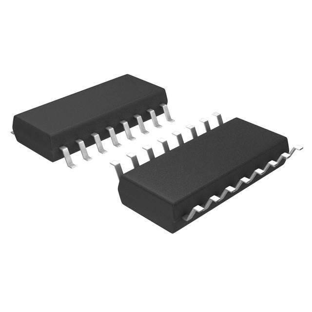
| 产品图片 |
|
| rohs | 符合RoHS无铅 / 符合限制有害物质指令(RoHS)规范要求 |
| 产品系列 | 逻辑集成电路,触发器,Texas Instruments SN74LS175NSR74LS |
| 数据手册 | |
| 产品型号 | SN74LS175NSR |
| 不同V、最大CL时的最大传播延迟 | 25ns @ 5V, 15pF |
| 产品种类 | 触发器 |
| 传播延迟时间 | 25 ns |
| 低电平输出电流 | 8 mA |
| 元件数 | 1 |
| 其它名称 | 296-28719-6 |
| 功能 | 主复位 |
| 包装 | Digi-Reel® |
| 单位重量 | 200.700 mg |
| 商标 | Texas Instruments |
| 安装类型 | 表面贴装 |
| 安装风格 | SMD/SMT |
| 封装 | Reel |
| 封装/外壳 | 16-SOIC(0.209",5.30mm 宽) |
| 封装/箱体 | SOP-16 |
| 工作温度 | 0°C ~ 70°C (TA) |
| 工厂包装数量 | 2000 |
| 最大工作温度 | + 70 C |
| 最小工作温度 | 0 C |
| 极性 | Inverting/Non-Inverting |
| 标准包装 | 1 |
| 每元件位数 | 4 |
| 电压-电源 | 4.75 V ~ 5.25 V |
| 电流-输出高,低 | 400µA, 8mA |
| 电流-静态 | 18mA |
| 电源电压-最大 | 5.25 V |
| 电源电压-最小 | 4.75 V |
| 电路数量 | 4 |
| 类型 | D 型 |
| 系列 | SN74LS175 |
| 触发器类型 | 正边沿 |
| 输入电容 | - |
| 输入类型 | TTL |
| 输入线路数量 | 2 |
| 输出类型 | 差分 |
| 输出线路数量 | 2 |
| 逻辑类型 | D-Type Flip-Flop |
| 逻辑系列 | LS |
| 频率-时钟 | 40MHz |
| 高电平输出电流 | - 0.4 mA |


- 商务部:美国ITC正式对集成电路等产品启动337调查
- 曝三星4nm工艺存在良率问题 高通将骁龙8 Gen1或转产台积电
- 太阳诱电将投资9.5亿元在常州建新厂生产MLCC 预计2023年完工
- 英特尔发布欧洲新工厂建设计划 深化IDM 2.0 战略
- 台积电先进制程称霸业界 有大客户加持明年业绩稳了
- 达到5530亿美元!SIA预计今年全球半导体销售额将创下新高
- 英特尔拟将自动驾驶子公司Mobileye上市 估值或超500亿美元
- 三星加码芯片和SET,合并消费电子和移动部门,撤换高东真等 CEO
- 三星电子宣布重大人事变动 还合并消费电子和移动部门
- 海关总署:前11个月进口集成电路产品价值2.52万亿元 增长14.8%


PDF Datasheet 数据手册内容提取
SN54174, SN54175, SN54LS174, SN54LS175, SN54S174, SN54S175, SN74174, SN74175, SN74LS174, SN74LS175, SN74S174, SN74S175 HEX/QUADRUPLE D-TYPE FLIP-FLOPS WITH CLEAR SDLS068A – DECEMBER 1972 – REVISED OCTOBER 2001 PRODUCTION DATA information is current as of publication date. Copyright 2001, Texas Instruments Incorporated Products conform to specifications per the terms of Texas Instruments standard warranty. Production processing does not necessarily include testing of all parameters. POST OFFICE BOX 655303 • DALLAS, TEXAS 75265 1
SN54174, SN54175, SN54LS174, SN54LS175, SN54S174, SN54S175, SN74174, SN74175, SN74LS174, SN74LS175, SN74S174, SN74S175 HEX/QUADRUPLE D-TYPE FLIP-FLOPS WITH CLEAR SDLS068A – DECEMBER 1972 – REVISED OCTOBER 2001 2 POST OFFICE BOX 655303 • DALLAS, TEXAS 75265
SN54174, SN54175, SN54LS174, SN54LS175, SN54S174, SN54S175, SN74174, SN74175, SN74LS174, SN74LS175, SN74S174, SN74S175 HEX/QUADRUPLE D-TYPE FLIP-FLOPS WITH CLEAR SDLS068A – DECEMBER 1972 – REVISED OCTOBER 2001 POST OFFICE BOX 655303 • DALLAS, TEXAS 75265 3
SN54174, SN54175, SN74174, SN74175 HEX/QUADRUPLE D-TYPE FLIP-FLOPS WITH CLEAR SDLS068A – DECEMBER 1972 – REVISED OCTOBER 2001 4 POST OFFICE BOX 655303 • DALLAS, TEXAS 75265
SN54LS174, SN54LS175, SN74LS174, SN74LS175 HEX/QUADRUPLE D-TYPE FLIP-FLOPS WITH CLEAR SDLS068A – DECEMBER 1972 – REVISED OCTOBER 2001 POST OFFICE BOX 655303 • DALLAS, TEXAS 75265 5
SN54S174, SN54S175, SN74S174, SN74S175 HEX/QUADRUPLE D-TYPE FLIP-FLOPS WITH CLEAR SDLS068A – DECEMBER 1972 – REVISED OCTOBER 2001 6 POST OFFICE BOX 655303 • DALLAS, TEXAS 75265
PACKAGE OPTION ADDENDUM www.ti.com 6-Feb-2020 PACKAGING INFORMATION Orderable Device Status Package Type Package Pins Package Eco Plan Lead/Ball Finish MSL Peak Temp Op Temp (°C) Device Marking Samples (1) Drawing Qty (2) (6) (3) (4/5) JM38510/07105BEA ACTIVE CDIP J 16 1 TBD Call TI N / A for Pkg Type -55 to 125 JM38510/ 07105BEA JM38510/07105BFA ACTIVE CFP W 16 1 TBD Call TI N / A for Pkg Type -55 to 125 JM38510/ 07105BFA JM38510/07106BEA ACTIVE CDIP J 16 1 TBD Call TI N / A for Pkg Type -55 to 125 JM38510/ 07106BEA JM38510/30106B2A ACTIVE LCCC FK 20 1 TBD POST-PLATE N / A for Pkg Type -55 to 125 JM38510/ 30106B2A JM38510/30106BEA ACTIVE CDIP J 16 1 TBD Call TI N / A for Pkg Type -55 to 125 JM38510/ 30106BEA JM38510/30106BFA ACTIVE CFP W 16 1 TBD Call TI N / A for Pkg Type -55 to 125 JM38510/ 30106BFA JM38510/30107B2A ACTIVE LCCC FK 20 1 TBD POST-PLATE N / A for Pkg Type -55 to 125 JM38510/ 30107B2A JM38510/30107BEA ACTIVE CDIP J 16 1 TBD Call TI N / A for Pkg Type -55 to 125 JM38510/ 30107BEA JM38510/30107BFA ACTIVE CFP W 16 1 TBD Call TI N / A for Pkg Type -55 to 125 JM38510/ 30107BFA M38510/07105BEA ACTIVE CDIP J 16 1 TBD Call TI N / A for Pkg Type -55 to 125 JM38510/ 07105BEA M38510/07105BFA ACTIVE CFP W 16 1 TBD Call TI N / A for Pkg Type -55 to 125 JM38510/ 07105BFA M38510/07106BEA ACTIVE CDIP J 16 1 TBD Call TI N / A for Pkg Type -55 to 125 JM38510/ 07106BEA M38510/30106B2A ACTIVE LCCC FK 20 1 TBD POST-PLATE N / A for Pkg Type -55 to 125 JM38510/ 30106B2A M38510/30106BEA ACTIVE CDIP J 16 1 TBD Call TI N / A for Pkg Type -55 to 125 JM38510/ 30106BEA M38510/30106BFA ACTIVE CFP W 16 1 TBD Call TI N / A for Pkg Type -55 to 125 JM38510/ 30106BFA M38510/30107B2A ACTIVE LCCC FK 20 1 TBD POST-PLATE N / A for Pkg Type -55 to 125 JM38510/ 30107B2A M38510/30107BEA ACTIVE CDIP J 16 1 TBD Call TI N / A for Pkg Type -55 to 125 JM38510/ 30107BEA Addendum-Page 1
PACKAGE OPTION ADDENDUM www.ti.com 6-Feb-2020 Orderable Device Status Package Type Package Pins Package Eco Plan Lead/Ball Finish MSL Peak Temp Op Temp (°C) Device Marking Samples (1) Drawing Qty (2) (6) (3) (4/5) M38510/30107BFA ACTIVE CFP W 16 1 TBD Call TI N / A for Pkg Type -55 to 125 JM38510/ 30107BFA SN54LS174J ACTIVE CDIP J 16 1 TBD Call TI N / A for Pkg Type -55 to 125 SN54LS174J SN54LS175J ACTIVE CDIP J 16 1 TBD Call TI N / A for Pkg Type -55 to 125 SN54LS175J SN54S174J ACTIVE CDIP J 16 1 TBD Call TI N / A for Pkg Type -55 to 125 SN54S174J SN54S175J ACTIVE CDIP J 16 1 TBD Call TI N / A for Pkg Type -55 to 125 SN54S175J SN74LS174D ACTIVE SOIC D 16 40 Green (RoHS NIPDAU Level-1-260C-UNLIM 0 to 70 LS174 & no Sb/Br) SN74LS174DR ACTIVE SOIC D 16 2500 Green (RoHS NIPDAU Level-1-260C-UNLIM 0 to 70 LS174 & no Sb/Br) SN74LS174N ACTIVE PDIP N 16 25 Green (RoHS NIPDAU N / A for Pkg Type 0 to 70 SN74LS174N & no Sb/Br) SN74LS174NSR ACTIVE SO NS 16 2000 Green (RoHS NIPDAU Level-1-260C-UNLIM 0 to 70 74LS174 & no Sb/Br) SN74LS175D ACTIVE SOIC D 16 40 Green (RoHS NIPDAU Level-1-260C-UNLIM 0 to 70 LS175 & no Sb/Br) SN74LS175DR ACTIVE SOIC D 16 2500 Green (RoHS NIPDAU Level-1-260C-UNLIM 0 to 70 LS175 & no Sb/Br) SN74LS175N ACTIVE PDIP N 16 25 Green (RoHS NIPDAU N / A for Pkg Type 0 to 70 SN74LS175N & no Sb/Br) SN74LS175NE4 ACTIVE PDIP N 16 25 Green (RoHS NIPDAU N / A for Pkg Type 0 to 70 SN74LS175N & no Sb/Br) SN74LS175NSR ACTIVE SO NS 16 2000 Green (RoHS NIPDAU Level-1-260C-UNLIM 0 to 70 74LS175 & no Sb/Br) SN74S175D ACTIVE SOIC D 16 40 Green (RoHS NIPDAU Level-1-260C-UNLIM 0 to 70 S175 & no Sb/Br) SN74S175N ACTIVE PDIP N 16 25 Green (RoHS NIPDAU N / A for Pkg Type 0 to 70 SN74S175N & no Sb/Br) SNJ54LS174FK ACTIVE LCCC FK 20 1 TBD POST-PLATE N / A for Pkg Type -55 to 125 SNJ54LS 174FK SNJ54LS174J ACTIVE CDIP J 16 1 TBD Call TI N / A for Pkg Type -55 to 125 SNJ54LS174J SNJ54LS174W ACTIVE CFP W 16 1 TBD Call TI N / A for Pkg Type -55 to 125 SNJ54LS174W Addendum-Page 2
PACKAGE OPTION ADDENDUM www.ti.com 6-Feb-2020 Orderable Device Status Package Type Package Pins Package Eco Plan Lead/Ball Finish MSL Peak Temp Op Temp (°C) Device Marking Samples (1) Drawing Qty (2) (6) (3) (4/5) SNJ54LS175FK ACTIVE LCCC FK 20 1 TBD POST-PLATE N / A for Pkg Type -55 to 125 SNJ54LS 175FK SNJ54LS175J ACTIVE CDIP J 16 1 TBD Call TI N / A for Pkg Type -55 to 125 SNJ54LS175J SNJ54LS175W ACTIVE CFP W 16 1 TBD Call TI N / A for Pkg Type -55 to 125 SNJ54LS175W SNJ54S174J ACTIVE CDIP J 16 1 TBD Call TI N / A for Pkg Type -55 to 125 SNJ54S174J SNJ54S174W ACTIVE CFP W 16 1 TBD Call TI N / A for Pkg Type -55 to 125 SNJ54S174W SNJ54S175J ACTIVE CDIP J 16 1 TBD Call TI N / A for Pkg Type -55 to 125 SNJ54S175J (1) The marketing status values are defined as follows: ACTIVE: Product device recommended for new designs. LIFEBUY: TI has announced that the device will be discontinued, and a lifetime-buy period is in effect. NRND: Not recommended for new designs. Device is in production to support existing customers, but TI does not recommend using this part in a new design. PREVIEW: Device has been announced but is not in production. Samples may or may not be available. OBSOLETE: TI has discontinued the production of the device. (2) RoHS: TI defines "RoHS" to mean semiconductor products that are compliant with the current EU RoHS requirements for all 10 RoHS substances, including the requirement that RoHS substance do not exceed 0.1% by weight in homogeneous materials. Where designed to be soldered at high temperatures, "RoHS" products are suitable for use in specified lead-free processes. TI may reference these types of products as "Pb-Free". RoHS Exempt: TI defines "RoHS Exempt" to mean products that contain lead but are compliant with EU RoHS pursuant to a specific EU RoHS exemption. Green: TI defines "Green" to mean the content of Chlorine (Cl) and Bromine (Br) based flame retardants meet JS709B low halogen requirements of <=1000ppm threshold. Antimony trioxide based flame retardants must also meet the <=1000ppm threshold requirement. (3) MSL, Peak Temp. - The Moisture Sensitivity Level rating according to the JEDEC industry standard classifications, and peak solder temperature. (4) There may be additional marking, which relates to the logo, the lot trace code information, or the environmental category on the device. (5) Multiple Device Markings will be inside parentheses. Only one Device Marking contained in parentheses and separated by a "~" will appear on a device. If a line is indented then it is a continuation of the previous line and the two combined represent the entire Device Marking for that device. (6) Lead/Ball Finish - Orderable Devices may have multiple material finish options. Finish options are separated by a vertical ruled line. Lead/Ball Finish values may wrap to two lines if the finish value exceeds the maximum column width. Important Information and Disclaimer:The information provided on this page represents TI's knowledge and belief as of the date that it is provided. TI bases its knowledge and belief on information provided by third parties, and makes no representation or warranty as to the accuracy of such information. Efforts are underway to better integrate information from third parties. TI has taken and Addendum-Page 3
PACKAGE OPTION ADDENDUM www.ti.com 6-Feb-2020 continues to take reasonable steps to provide representative and accurate information but may not have conducted destructive testing or chemical analysis on incoming materials and chemicals. TI and TI suppliers consider certain information to be proprietary, and thus CAS numbers and other limited information may not be available for release. In no event shall TI's liability arising out of such information exceed the total purchase price of the TI part(s) at issue in this document sold by TI to Customer on an annual basis. OTHER QUALIFIED VERSIONS OF SN54LS174, SN54LS175, SN54S175, SN74LS174, SN74LS175, SN74S175 : •Catalog: SN74LS174, SN74LS175, SN74S175 •Military: SN54LS174, SN54LS175, SN54S175 NOTE: Qualified Version Definitions: •Catalog - TI's standard catalog product •Military - QML certified for Military and Defense Applications Addendum-Page 4
PACKAGE MATERIALS INFORMATION www.ti.com 14-Jul-2012 TAPE AND REEL INFORMATION *Alldimensionsarenominal Device Package Package Pins SPQ Reel Reel A0 B0 K0 P1 W Pin1 Type Drawing Diameter Width (mm) (mm) (mm) (mm) (mm) Quadrant (mm) W1(mm) SN74LS174DR SOIC D 16 2500 330.0 16.4 6.5 10.3 2.1 8.0 16.0 Q1 SN74LS174NSR SO NS 16 2000 330.0 16.4 8.2 10.5 2.5 12.0 16.0 Q1 SN74LS175DR SOIC D 16 2500 330.0 16.4 6.5 10.3 2.1 8.0 16.0 Q1 SN74LS175NSR SO NS 16 2000 330.0 16.4 8.2 10.5 2.5 12.0 16.0 Q1 PackMaterials-Page1
PACKAGE MATERIALS INFORMATION www.ti.com 14-Jul-2012 *Alldimensionsarenominal Device PackageType PackageDrawing Pins SPQ Length(mm) Width(mm) Height(mm) SN74LS174DR SOIC D 16 2500 333.2 345.9 28.6 SN74LS174NSR SO NS 16 2000 367.0 367.0 38.0 SN74LS175DR SOIC D 16 2500 333.2 345.9 28.6 SN74LS175NSR SO NS 16 2000 367.0 367.0 38.0 PackMaterials-Page2
IMPORTANTNOTICEANDDISCLAIMER TI PROVIDES TECHNICAL AND RELIABILITY DATA (INCLUDING DATASHEETS), DESIGN RESOURCES (INCLUDING REFERENCE DESIGNS), APPLICATION OR OTHER DESIGN ADVICE, WEB TOOLS, SAFETY INFORMATION, AND OTHER RESOURCES “AS IS” AND WITH ALL FAULTS, AND DISCLAIMS ALL WARRANTIES, EXPRESS AND IMPLIED, INCLUDING WITHOUT LIMITATION ANY IMPLIED WARRANTIES OF MERCHANTABILITY, FITNESS FOR A PARTICULAR PURPOSE OR NON-INFRINGEMENT OF THIRD PARTY INTELLECTUAL PROPERTY RIGHTS. These resources are intended for skilled developers designing with TI products. You are solely responsible for (1) selecting the appropriate TI products for your application, (2) designing, validating and testing your application, and (3) ensuring your application meets applicable standards, and any other safety, security, or other requirements. These resources are subject to change without notice. TI grants you permission to use these resources only for development of an application that uses the TI products described in the resource. Other reproduction and display of these resources is prohibited. No license is granted to any other TI intellectual property right or to any third party intellectual property right. TI disclaims responsibility for, and you will fully indemnify TI and its representatives against, any claims, damages, costs, losses, and liabilities arising out of your use of these resources. TI’s products are provided subject to TI’s Terms of Sale (www.ti.com/legal/termsofsale.html) or other applicable terms available either on ti.com or provided in conjunction with such TI products. TI’s provision of these resources does not expand or otherwise alter TI’s applicable warranties or warranty disclaimers for TI products. Mailing Address: Texas Instruments, Post Office Box 655303, Dallas, Texas 75265 Copyright © 2020, Texas Instruments Incorporated