ICGOO在线商城 > 集成电路(IC) > 逻辑 - 移位寄存器 > SN74HC594DT
 Datasheet下载
- 型号: SN74HC594DT
- 制造商: Texas Instruments
- 库位|库存: xxxx|xxxx
- 要求:
| 数量阶梯 | 香港交货 | 国内含税 |
| +xxxx | $xxxx | ¥xxxx |
查看当月历史价格
查看今年历史价格
SN74HC594DT产品简介:
ICGOO电子元器件商城为您提供SN74HC594DT由Texas Instruments设计生产,在icgoo商城现货销售,并且可以通过原厂、代理商等渠道进行代购。 SN74HC594DT价格参考。Texas InstrumentsSN74HC594DT封装/规格:逻辑 - 移位寄存器, 。您可以下载SN74HC594DT参考资料、Datasheet数据手册功能说明书,资料中有SN74HC594DT 详细功能的应用电路图电压和使用方法及教程。
SN74HC594DT是Texas Instruments(德州仪器)生产的一款8位移位寄存器,属于逻辑电路中的移位寄存器系列。它具有串行输入、并行输出的功能,并且内置了存储寄存器和三态输出缓冲器,广泛应用于各种数字电路设计中。

 应用场景

1. LED显示屏驱动:
   SN74HC594DT常用于驱动LED显示屏或LED灯带。通过串行输入数据,可以逐个控制多个LED的亮灭状态。由于其具备8位并行输出功能,能够同时控制8个LED,多个SN74HC594DT级联使用可以扩展到更多LED。例如,在交通信号灯、广告牌、舞台灯光等场合,它能有效简化电路设计,减少所需的微控制器引脚数量。

2. 键盘扫描与矩阵处理:
   在键盘或按键矩阵的设计中,SN74HC594DT可以用作行扫描信号的生成器。通过串行输入控制信号,依次激活每一行,然后读取列信号以确定哪个按键被按下。这种方式可以大大减少所需的I/O引脚数量,特别适用于多按键设备如计算器、遥控器等。

3. 电机控制:
   对于步进电机或其他需要精确时序控制的电机,SN74HC594DT可以通过串行接口接收指令,将数据转换为并行输出,从而控制电机的各个相位。这种应用常见于自动化设备、机器人等领域。

4. 数据传输与扩展:
   在一些需要扩展I/O端口的应用中,SN74HC594DT可以作为I/O扩展芯片使用。它能够将来自微控制器的串行数据转换为并行输出,或者将并行输入的数据转换为串行输出,适用于数据采集系统、传感器网络等场景。

5. 音频信号处理:
   在某些音频设备中,SN74HC594DT可以用于处理音频信号的串行传输或并行输出,特别是在需要多位并行输出的场合,如多通道音频放大器或音效处理器。

总之,SN74HC594DT凭借其高效的数据传输能力和灵活的接口特性,成为众多数字电路设计中的重要组件,适用于多种应用场景。
| 参数 | 数值 |
| 产品目录 | 集成电路 (IC)半导体 |
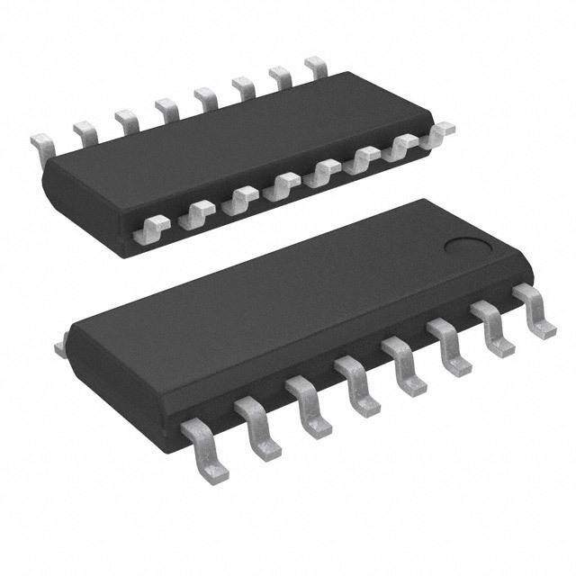
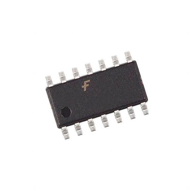
| 描述 | IC SHIFT REGISTER 8BIT 16-SOIC计数器移位寄存器 8-Bit Shift Register w/Output Registers |
| 产品分类 | |
| 品牌 | Texas Instruments |
| 产品手册 | |
| 产品图片 |
|
| rohs | 符合RoHS无铅 / 符合限制有害物质指令(RoHS)规范要求 |
| 产品系列 | 逻辑集成电路,计数器移位寄存器,Texas Instruments SN74HC594DT74HC |
| 数据手册 | |
| 产品型号 | SN74HC594DT |
| 产品种类 | 计数器移位寄存器 |
| 传播延迟时间 | 150 ns, 30 ns, 25 ns |
| 供应商器件封装 | 16-SOIC N |
| 元件数 | 1 |
| 其它名称 | 296-31820-1 |
| 功能 | 串行至并行 |
| 包装 | 剪切带 (CT) |
| 单位重量 | 140 mg |
| 商标 | Texas Instruments |
| 安装类型 | 表面贴装 |
| 安装风格 | SMD/SMT |
| 封装 | Reel |
| 封装/外壳 | 16-SOIC(0.154",3.90mm 宽) |
| 封装/箱体 | SOIC-16 |
| 工作温度 | -40°C ~ 85°C |
| 工作电源电压 | 5 V |
| 工厂包装数量 | 250 |
| 最大工作温度 | + 85 C |
| 最小工作温度 | - 40 C |
| 标准包装 | 1 |
| 每元件位数 | 8 |
| 电压-电源 | 2 V ~ 6 V |
| 电源电压-最大 | 6 V |
| 电源电压-最小 | 2 V |
| 电路数量 | 1 |
| 系列 | SN74HC594 |
| 计数顺序 | Serial to Serial/Parallel |
| 输入线路数量 | 1 |
| 输出类型 | 推挽式 |
| 输出线路数量 | 9 |
| 逻辑类型 | 移位寄存器 |
| 逻辑系列 | HC |


- 商务部:美国ITC正式对集成电路等产品启动337调查
- 曝三星4nm工艺存在良率问题 高通将骁龙8 Gen1或转产台积电
- 太阳诱电将投资9.5亿元在常州建新厂生产MLCC 预计2023年完工
- 英特尔发布欧洲新工厂建设计划 深化IDM 2.0 战略
- 台积电先进制程称霸业界 有大客户加持明年业绩稳了
- 达到5530亿美元!SIA预计今年全球半导体销售额将创下新高
- 英特尔拟将自动驾驶子公司Mobileye上市 估值或超500亿美元
- 三星加码芯片和SET,合并消费电子和移动部门,撤换高东真等 CEO
- 三星电子宣布重大人事变动 还合并消费电子和移动部门
- 海关总署:前11个月进口集成电路产品价值2.52万亿元 增长14.8%


PDF Datasheet 数据手册内容提取
Product Sample & Technical Tools & Support & Folder Buy Documents Software Community SN54HC594,SN74HC594 SCLS040G–DECEMBER1982–REVISEDMARCH2015 SNx4HC594 8-Bit Shift Registers With Output Registers 1 Features 3 Description • WideOperatingVoltageRangeof2Vto6V The SNx4HC594 devices contain an 8-bit serial-in, 1 parallel-out shift register that feeds an 8-bit D-type • High-CurrentOutputsCanDriveupto storage register. Separate clocks and direct 15LSTTLLoads overriding clear (RCLR, SRCLR) inputs are provided • LowPowerConsumption,80-µAMaximumI on both the shift and storage registers. A serial (Q ) CC H’ • Typicalt =15ns outputisprovidedforcascadingpurposes. pd • ±6-mAOutputDriveat5V Both the shift register (SRCLK) and storage register (RCLK) clocks are positive edge triggered. If both • LowInputCurrentof1 µAMaximum clocks are connected together, the shift register • 8-BitSerial-In,Parallel-OutShiftRegistersWith always is one count pulse ahead of the storage Storage register. • IndependentDirectOverridingClearsonShiftand The parallel (Q − Q ) outputs have high-current StorageRegisters A H capability.Q isastandardoutput. H’ • IndependentClocksforBothShiftand StorageRegisters DeviceInformation(1) PARTNUMBER PACKAGE BODYSIZE(NOM) 2 Applications PDIP(16) 19.30mm×6.35mm • ProAudioMixer SN74HC594 9.00mm×9.00mm SOIC(16) • ElevatorsandEscalators 10.30mm×7.50mm • HumanMachineInterface(HMI):Industrial (1) For all available packages, see the orderable addendum at Monitor theendofthedatasheet. • EntertainmentSystems LogicDiagram(PositiveLogic) • GridInfrastructure:GridControl 13 • AccessControlandSecurity:DVRandDVS RCLR RCLK 12 10 SRCLR SRCLK 11 SER 14 1D R3R 15 C1 C3 QA R 3S 2S R 2R 3R 1 C2 C3 QB R 3S 2S R 2R 3R 2 C2 C3 QC R 3S 2S R 2RC2 3RC3 3 QD R 3S 2S R 2R 3R 4 C2 C3 QE R 3S 2S R 2R 3R 5 C2 C3 QF R 3S 2S R 2R 3R 6 C2 C3 QG R 3S 2S R 2R 3R 7 C2 C3 QH R 3S 9 QH′ PinnumbersshownarefortheD,DW,J,N,andWpackages. 1 An IMPORTANT NOTICE at the end of this data sheet addresses availability, warranty, changes, use in safety-critical applications, intellectualpropertymattersandotherimportantdisclaimers.UNLESSOTHERWISENOTED,thisdocumentcontainsPRODUCTION DATA.
SN54HC594,SN74HC594 SCLS040G–DECEMBER1982–REVISEDMARCH2015 www.ti.com Table of Contents 1 Features.................................................................. 1 8.1 Overview.................................................................11 2 Applications........................................................... 1 8.2 FunctionalBlockDiagram.......................................11 3 Description............................................................. 1 8.3 FeatureDescription.................................................11 8.4 DeviceFunctionalModes........................................12 4 RevisionHistory..................................................... 2 9 ApplicationandImplementation........................ 13 5 PinConfigurationandFunctions......................... 3 9.1 ApplicationInformation............................................13 6 Specifications......................................................... 4 9.2 TypicalApplication .................................................13 6.1 AbsoluteMaximumRatings......................................4 10 PowerSupplyRecommendations..................... 15 6.2 ESDRatings..............................................................4 11 Layout................................................................... 15 6.3 RecommendedOperatingConditions.......................4 6.4 ThermalInformation..................................................5 11.1 LayoutGuidelines.................................................15 6.5 ElectricalCharacteristics...........................................5 11.2 LayoutExample....................................................15 6.6 SwitchingCharacteristics:C =50pF.......................6 12 DeviceandDocumentationSupport................. 16 L 6.7 SwitchingCharacteristics:C =150pF....................6 12.1 DocumentationSupport........................................16 L 6.8 TimingRequirements................................................7 12.2 Trademarks...........................................................16 6.9 OperatingCharacteristics..........................................7 12.3 ElectrostaticDischargeCaution............................16 6.10 TypicalCharacteristics............................................9 12.4 Glossary................................................................16 7 ParameterMeasurementInformation................10 13 Mechanical,Packaging,andOrderable Information........................................................... 16 8 DetailedDescription............................................ 11 4 Revision History ChangesfromRevisionF(October2003)toRevisionG Page • AddedPinConfigurationandFunctionssection,ESDRatingstable,FeatureDescriptionsection,DeviceFunctional Modes,ApplicationandImplementationsection,PowerSupplyRecommendationssection,Layoutsection,Device andDocumentationSupportsection,andMechanical,Packaging,andOrderableInformationsection .............................. 1 • Removedorderinginformation............................................................................................................................................... 1 • ESDwarningadded................................................................................................................................................................ 1 2 SubmitDocumentationFeedback Copyright©1982–2015,TexasInstrumentsIncorporated SN74HC594
SN54HC594,SN74HC594 www.ti.com SCLS040G–DECEMBER1982–REVISEDMARCH2015 5 Pin Configuration and Functions D,DW,orNPackage 16-PINPDIPorSOIC TopView QB 1 16 VCC QC 2 15 QA QD 3 14 SER QE 4 13 RCLR Q 5 12 RCLK F Q 6 11 SRCLK G Q 7 10 SRCLR H GND 8 9 QH′ PinFunctions PIN I/O DESCRIPTION NO. NAME 1 Q O OutputB B 2 Q O OutputC C 3 Q O OutputD D 4 Q O OutputE E 5 Q O OutputF F 6 Q O OutputG G 7 Q O OutputH H 8 GND – Ground 9 Q O Q inverted H' H 10 SRCLR I Serialclear 11 SRCLK I Serialclock 12 RCLK I Storageclock 13 RCLK I Storageclear 14 SER I Serialinput 15 Q O OutputA A 16 Vcc – Powerpin Copyright©1982–2015,TexasInstrumentsIncorporated SubmitDocumentationFeedback 3 SN74HC594
SN54HC594,SN74HC594 SCLS040G–DECEMBER1982–REVISEDMARCH2015 www.ti.com 6 Specifications 6.1 Absolute Maximum Ratings(1) overoperatingfree-airtemperaturerange(unlessotherwisenoted) MIN MAX UNIT V Supplyvoltage –0.5 7 V CC I Inputclampcurrent(2) V <0orV >V –20 20 mA IK I I CC I Outputclampcurrent(2) V <0orV >V –20 20 mA OK O O CC I Continuousoutputcurrent V =0toV –35 35 mA O O CC ContinuouscurrentthroughV orGND –70 70 mA CC Dpackage 73 θ Packagethermalimpedance(3) DWpackage 57 °C/W JA Npackage 67 T Storagetemperature –60 150 °C stg (1) StressesbeyondthoselistedunderAbsoluteMaximumRatingsmaycausepermanentdamagetothedevice.Thesearestressratings only,whichdonotimplyfunctionaloperationofthedeviceattheseoranyotherconditionsbeyondthoseindicatedunderRecommended OperatingConditions.Exposuretoabsolute-maximum-ratedconditionsforextendedperiodsmayaffectdevicereliability. (2) Theinputandoutputvoltageratingsmaybeexceedediftheinputandoutputcurrentratingsareobserved. (3) ThepackagethermalimpedanceiscalculatedinaccordancewithJESD51-7. 6.2 ESD Ratings VALUE UNIT Humanbodymodel(HBM),perANSI/ESDA/JEDECJS-001(1) ±2000 V(ESD) Electrostaticdischarge Charged-devicemodel(CDM),perJEDECspecificationJESD22- ±1000 V C101(2) (1) JEDECdocumentJEP155statesthat500-VHBMallowssafemanufacturingwithastandardESDcontrolprocess. (2) JEDECdocumentJEP157statesthat250-VCDMallowssafemanufacturingwithastandardESDcontrolprocess. 6.3 Recommended Operating Conditions overoperatingfree-airtemperaturerange(unlessotherwisenoted)(1) SN54HC594(2) SN74HC594 UNIT MIN NOM MAX MIN NOM MAX V Supplyvoltage 2 5 6 2 5 6 V CC V =2V 1.5 1.5 CC V High-levelinputvoltage V =4.5V 3.15 3.15 V IH CC V =6V 4.2 4.2 CC V =2V 0.5 0.5 CC V Low-levelinputvoltage V =4.5V 1.35 1.35 V IL CC V =6V 1.8 1.8 CC V Inputvoltage 0 V 0 V V I CC CC V Outputvoltage 0 V 0 V V O CC CC V =2V 1000 1000 CC t Inputtransition(riseandfall)rate V =4.5V 500 500 ns t CC V =6V 400 400 CC T Operatingfree-airtemperature –55 125 –40 125 °C A (1) AllunusedinputsofthedevicemustbeheldatV orGNDtoensureproperdeviceoperation.RefertotheTIapplicationreport, CC ImplicationsofSloworFloatingCMOSInputs,SCBA004. (2) ProductPreview 4 SubmitDocumentationFeedback Copyright©1982–2015,TexasInstrumentsIncorporated SN74HC594
SN54HC594,SN74HC594 www.ti.com SCLS040G–DECEMBER1982–REVISEDMARCH2015 6.4 Thermal Information SN74HC594 THERMALMETRIC(1) N(PDIP) D(SOIC) DW(SOIC) UNIT 16PINS 16PINS 16PINS R Junction-to-ambientthermalresistance 41.3 72.3 71 θJA R Junction-to-case(top)thermalresistance 28 33.2 32.3 θJC(top) R Junction-to-boardthermalresistance 21.3 29.9 35.9 °C/W θJB ψ Junction-to-topcharacterizationparameter 12.6 5.3 6.7 JT ψ Junction-to-boardcharacterizationparameter 21.1 29.6 35.3 JB (1) Formoreinformationabouttraditionalandnewthermalmetrics,seetheICPackageThermalMetricsapplicationreport,SPRA953. 6.5 Electrical Characteristics overrecommendedoperatingfree-airtemperaturerange(unlessotherwisenoted) SN54HC594(1) SN74HC594 SN74HC594 PARAMETER TESTCONDITIONS VCC TA=25°C –55°Cto125°C –40°Cto85°C –40°Cto125°C UNIT MIN TYP MAX MIN MAX MIN MAX MIN MAX 2V 1.9 1.998 1.9 1.9 1.9 IOH=–20µA 4.5V 4.4 4.499 4.4 4.4 4.4 6V 5.9 5.999 5.9 5.9 5.9 VOH VorI=VIVLIH QQHA’–QH IIOOHH==––64mmAA 4.5V 33..9988 44..33 33..77 33..8844 33..8844 V QH’ ImOHA=–5.2 5.48 5.8 5.2 5.34 5.34 6V QA–QH ImOHA=–7.8 5.48 5.8 5.2 5.34 5.34 2V 0.002 0.1 0.1 0.1 0.1 IOL=20µA 4.5V 0.001 0.1 0.1 0.1 0.1 6V 0.001 0.1 0.1 0.1 0.1 VOL VorI=VIVLIH QQHA’–QH IIOOLL==64mmAA 4.5V 00..1177 00..2266 00..44 00..3333 00..3333 V QH’ ImOLA=5.2 0.15 0.26 0.4 0.33 0.33 6V QA–QH ImOLA=7.8 0.15 0.26 0.4 0.33 0.33 II VI=VCCor0 6V ±0.1 ±100 ±1000 ±1000 ±1000 nA ICC VorI=0,VCC IO=0 6V 8 160 80 80 µA 2Vto Ci 6V 3 10 10 10 pF (1) ProductPreview Copyright©1982–2015,TexasInstrumentsIncorporated SubmitDocumentationFeedback 5 SN74HC594
SN54HC594,SN74HC594 SCLS040G–DECEMBER1982–REVISEDMARCH2015 www.ti.com 6.6 Switching Characteristics:C =50pF L overrecommendedoperatingfree-airtemperaturerange(unlessotherwisenoted)(seeFigure4) SN54HC594(1) SN74HC594 SN74HC594 PARAMETER (IFNRPOUMT) (OUTTOPUT) VCC TA=25°C –55°Cto125°C –40°Cto85°C –40°Cto125°C UNIT MIN TYP MAX MIN MAX MIN MAX MIN MAX 2V 5 8 3.3 4 4 fmax 4.5V 25 35 17 20 20 MHz 6V 29 40 20 24 24 2V 50 150 225 185 200 SRCLK QH’ 4.5V 20 30 45 37 42 6V 15 25 38 31 36 tpd ns 2V 50 150 225 185 200 RCLK QA–QH 4.5V 20 30 45 37 42 6V 15 25 38 31 36 2V 50 150 225 185 200 SRCLR QH’ 4.5V 20 30 45 37 42 6V 15 25 38 31 36 tPHL ns 2V 50 125 185 155 170 RCLR QA–QH 4.5V 20 25 37 31 36 6V 15 21 31 26 31 2V 38 75 110 95 110 QH’ 4.5V 8 15 22 19 21 6V 6 13 19 16 18 tt ns 2V 38 60 90 75 85 QA–QH 4.5V 8 12 18 15 17 6V 6 10 15 13 15 (1) ProductPreview 6.7 Switching Characteristics: C = 150 pF L overrecommendedoperatingfree-airtemperaturerange(unlessotherwisenoted)(seeFigure4) SN54HC594(1) SN74HC594 SN74HC594 PARAMETER (IFNRPOUMT) (OUTTOPUT) VCC TA=25°C –55°Cto125°C –40°Cto85°C –40°Cto125°C UNIT MIN TYP MAX MIN MAX MIN MAX MIN MAX 2V 90 200 300 250 270 tpd RCLK QA–QH 4.5V 23 40 60 50 55 ns 6V 19 34 51 43 48 2V 90 200 300 250 270 tPHL RCLR QA–QH 4.5V 23 40 60 50 55 ns 6V 19 34 51 43 48 2V 45 210 315 265 285 tt QA–QH 4.5V 17 42 63 53 58 ns 6V 13 36 53 45 50 (1) ProductPreview 6 SubmitDocumentationFeedback Copyright©1982–2015,TexasInstrumentsIncorporated SN74HC594
SN54HC594,SN74HC594 www.ti.com SCLS040G–DECEMBER1982–REVISEDMARCH2015 6.8 Timing Requirements overrecommendedoperatingfree-airtemperaturerange(unlessotherwisenoted) SN54HC594(1) SN74HC594 SN74HC594 VCC TA=25°C –55°Cto125°C –40°Cto85°C –40°Cto125°C UNIT MIN MAX MIN MAX MIN MAX MIN MAX 2V 5 3.3 4 4 fclock Clockfrequency 4.5V 25 17 20 20 MHz 6V 29 20 24 24 2V 100 150 125 130 SRCLKorRCLKhighorlow 4.5V 20 30 25 27 Pulse 6V 17 25 21 23 tw duration 2V 100 150 125 130 ns SRCLRorRCLRlow 4.5V 20 30 25 27 6V 17 25 21 23 2V 90 135 110 115 SERbeforeSRCLK↑ 4.5V 18 27 22 24 6V 15 23 19 21 ns 2V 90 135 110 115 SRCLK↑beforeRCLK↑(2) 4.5V 18 27 22 24 6V 15 23 19 21 2V 50 75 63 68 Setuptime tsu beforeCLK↑ SRCLRlowbeforeRCLK↑ 4.5V 10 15 13 15 6V 9 13 11 13 2V 20 20 20 20 SRCLRhigh(inactive)before 4.5V 10 10 10 10 ns SRCLK↑ 6V 10 10 10 10 2V 5 5 5 5 RCLRhigh(inactive)before 4.5V 5 5 5 5 SRCLK↑ 6V 5 5 5 5 2V 5 5 5 5 th Holdtime,SERafterSRCLK↑ 4.5V 5 5 5 5 ns 6V 5 5 5 5 (1) ProductPreview (2) Thissetuptimeensuresthattheoutputregisterreceivesstabledatafromtheshift-registeroutputs.Theclocksmaybetiedtogether,in whichcasetheoutputregisterisoneclockpulsebehindtheshiftregister. 6.9 Operating Characteristics T =25°C A PARAMETER TESTCONDITIONS TYP UNIT C Powerdissipationcapacitance Noload 395 pF pd Copyright©1982–2015,TexasInstrumentsIncorporated SubmitDocumentationFeedback 7 SN74HC594
SN54HC594,SN74HC594 SCLS040G–DECEMBER1982–REVISEDMARCH2015 www.ti.com SRCLK SER RCLK SRCLR RCLR QA QB QC QD QE QF QG QH QH′ Figure1. TimingDiagram 8 SubmitDocumentationFeedback Copyright©1982–2015,TexasInstrumentsIncorporated SN74HC594
SN54HC594,SN74HC594 www.ti.com SCLS040G–DECEMBER1982–REVISEDMARCH2015 6.10 Typical Characteristics 30 60 25 50 20 40 s) s) n n D ( 15 D ( 30 P P T T 10 20 5 10 0 0 -100 -50 0 50 100 150 0 2 4 6 8 Temperature VCC D001 D002 Figure2.SN74HC594TPDvs.Temperature Figure3.SN74HC594TPDvs.VCC Copyright©1982–2015,TexasInstrumentsIncorporated SubmitDocumentationFeedback 9 SN74HC594
SN54HC594,SN74HC594 SCLS040G–DECEMBER1982–REVISEDMARCH2015 www.ti.com 7 Parameter Measurement Information VCC High-Level 50% 50% Pulse From Output Test 0 V UnderTest Point tw CL VCC (see NoteA) Low-Level 50% 50% Pulse 0 V LOAD CIRCUIT VOLTAGEWAVEFORMS PULSEDURATIONS VCC Input 50% 50% 0 V tPLH tPHL ReferIennpcuet 50% VCC InO-Puhtapsuet 105%0% 90% 90% 501%0% VOH 0 V VOL tsu th tr tf tPHL tPLH Data VCC VOH Input 50% 90% 90% 50% Out-of-Phase 90% 50% 50% 90% 10% 10% 0 V Output 10% 10% VOL tr tf tf tr VOLTAGEWAVEFORMS VOLTAGEWAVEFORMS SETUPANDHOLDANDINPUTRISEANDFALLTIMES PROPAGATION DELAYAND OUTPUT TRANSITION TIMES A. C includesprobeandtest-fixturecapacitance. L B. Phase relationships between waveforms were chosen arbitrarily. All input pulses are supplied by generators having thefollowingcharacteristics:PRR≤1MHz,Z =50Ω,t =6ns,t =6ns. O r f C. Forclockinputs,f ismeasuredwhentheinputdutycycleis50%. max D. Theoutputsaremeasuredoneatatimewithoneinputtransitionpermeasurement. E. t andt arethesameast . PLH PHL pd F. t andt arethesameast. f r t Figure4. LoadCircuitandVoltageWaveforms 10 SubmitDocumentationFeedback Copyright©1982–2015,TexasInstrumentsIncorporated SN74HC594
SN54HC594,SN74HC594 www.ti.com SCLS040G–DECEMBER1982–REVISEDMARCH2015 8 Detailed Description 8.1 Overview The SNx4HC594 devices contain an 8-bit serial-in, parallel-out shift register that feeds an 8-bit D-type storage register. Separate clocks and direct overriding clear (RCLR, SRCLR) inputs are provided on both the shift and storageregisters.Aserial(Q )outputisprovidedforcascadingpurposes. H’ Both the shift register (SRCLK) and storage register (RCLK) clocks are positive edge triggered. If both clocks are connectedtogether,theshiftregisteralwaysisonecountpulseaheadofthestorageregister. Theparallel(Q −Q )outputshavehigh-currentcapability.Q isastandardoutput. A H H’ 8.2 Functional Block Diagram 13 RCLR 12 RCLK 10 SRCLR 11 SRCLK 14 R SER 1D 3R 15 C1 C3 QA R 3S 2S R 2R 3R 1 C2 C3 QB R 3S 2S R 2R 3R 2 C2 C3 QC R 3S 2S R 2R 3R 3 C2 C3 QD R 3S 2S R 2R 3R 4 C2 C3 QE R 3S 2S R 2R 3R 5 C2 C3 QF R 3S 2S R 2R 3R 6 C2 C3 QG R 3S 2S R 2R 3R 7 C2 C3 QH R 3S 9 QH′ PinnumbersshownarefortheD,DW,J,N,andWpackages. Figure5. LogicDiagram(PositiveLogic) 8.3 Feature Description The wide operating range allows the device to be used in a variety of systems that use different logic levels. The high-current outputs allow the device to drive medium loads without significant drops in output voltage. In addition, the low power consumption makes this device a good choice for portable and battery power-sensitive applications. Copyright©1982–2015,TexasInstrumentsIncorporated SubmitDocumentationFeedback 11 SN74HC594
SN54HC594,SN74HC594 SCLS040G–DECEMBER1982–REVISEDMARCH2015 www.ti.com 8.4 Device Functional Modes Table1.FunctionTable INPUTS FUNCTION SER SRCLK SRCLR RCLK RCLR X X L X X Shiftregisteriscleared. Firststageofshiftregistergoeslow. L ↑ H X X Otherstagesstorethedataofpreviousstage,respectively. Firststageofshiftregistergoeshigh. H ↑ H X X Otherstagesstorethedataofpreviousstage,respectively. L ↓ H X X Shiftregisterstateisnotchanged. X X X X L Storageregisteriscleared. X X X ↑ H Shiftregisterdataisstoredinthestorageregister. X X X ↓ H Storageregisterstateisnotchanged. 12 SubmitDocumentationFeedback Copyright©1982–2015,TexasInstrumentsIncorporated SN74HC594
SN54HC594,SN74HC594 www.ti.com SCLS040G–DECEMBER1982–REVISEDMARCH2015 9 Application and Implementation NOTE Information in the following applications sections is not part of the TI component specification, and TI does not warrant its accuracy or completeness. TI’s customers are responsible for determining suitability of components for their purposes. Customers should validateandtesttheirdesignimplementationtoconfirmsystemfunctionality. 9.1 Application Information The SN74HC594 is a low drive CMOS device that can be used for a multitude of bus interface type applications where output ringing is a concern. The low drive and slow edge rates will minimize overshoot and undershoot on theoutputs. 9.2 Typical Application Figure6. TypicalApplicationSchematic 9.2.1 DesignRequirements ThisdeviceusesCMOStechnologyandhasbalancedoutputdrive.Takecaretoavoidbuscontentionbecauseit can drive currents that would exceed maximum limits. The high drive will also create fast edges into light loads soconsiderroutingandloadconditionstopreventringing. Copyright©1982–2015,TexasInstrumentsIncorporated SubmitDocumentationFeedback 13 SN74HC594
SN54HC594,SN74HC594 SCLS040G–DECEMBER1982–REVISEDMARCH2015 www.ti.com Typical Application (continued) 9.2.2 DetailedDesignProcedure • Recommendedinputconditions: – Risetimeandfalltimespecssee(Δt/ΔV)inRecommendedOperatingConditions table. – SpecifiedHighandlowlevels.See(V andV )inRecommendedOperatingConditions table. IH IL – Inputsareovervoltagetolerantallowingthemtogoashighas5.5VatanyvalidV CC • Recommendedoutputconditions: – Loadcurrentsshouldnotexceed35mAperoutputand70mAtotalforthepart – OutputsshouldnotbepulledaboveV CC 9.2.3 ApplicationCurves Figure7. SwitchingCharacteristicsComparison 14 SubmitDocumentationFeedback Copyright©1982–2015,TexasInstrumentsIncorporated SN74HC594
SN54HC594,SN74HC594 www.ti.com SCLS040G–DECEMBER1982–REVISEDMARCH2015 10 Power Supply Recommendations The power supply can be any voltage between the minimum and maximum supply voltage rating located in the RecommendedOperatingConditions. Each V terminal should have a good bypass capacitor to prevent power disturbance. For devices with a single CC supply, TI recommends a 0.1-μF capacitor and if there are multiple V terminals then TI recommends a 0.01-μF CC or 0.022-μF capacitor for each power terminal. Multiple bypass capacitors can be paralleled to reject different frequencies of noise. Frequencies of 0.1 μF and 1 μF are commonly used in parallel. The bypass capacitor shouldbeinstalledascloseaspossibletothepowerterminalforbestresults. 11 Layout 11.1 Layout Guidelines Whenusingmultiplebitlogicdevicesinputsshouldnoteverfloat. In many cases, functions or parts of functions of digital logic devices are unused, for example, when only two inputs of a triple-input AND gate are used or only three of the four buffer gates are used. Such input pins should not be left unconnected because the undefined voltages at the outside connections result in undefined operational states. Specified below are the rules that must be observed under all circumstances. All unused inputs of digital logic devices must be connected to a high or low bias to prevent them from floating. The logic level that should be applied to any particular unused input depends on the function of the device. Generally they will be tied to GND or V whichever make more sense or is more convenient. Floating outputs is generally CC acceptable, unless the part is a transceiver. If the transceiver has an output enable pin it will disable the outputs section of the part when asserted. This will not disable the input section of the I.O’s so they also cannot float whendisabled. 11.2 Layout Example Figure8. LayoutRecommendation Copyright©1982–2015,TexasInstrumentsIncorporated SubmitDocumentationFeedback 15 SN74HC594
SN54HC594,SN74HC594 SCLS040G–DECEMBER1982–REVISEDMARCH2015 www.ti.com 12 Device and Documentation Support 12.1 Documentation Support 12.1.1 RelatedDocumentation Forrelateddocumentationseethefollowing: ImplicationsofSloworFloatingCMOSInputs,SCBA004 12.2 Trademarks Alltrademarksarethepropertyoftheirrespectiveowners. 12.3 Electrostatic Discharge Caution Thesedeviceshavelimitedbuilt-inESDprotection.Theleadsshouldbeshortedtogetherorthedeviceplacedinconductivefoam duringstorageorhandlingtopreventelectrostaticdamagetotheMOSgates. 12.4 Glossary SLYZ022—TIGlossary. Thisglossarylistsandexplainsterms,acronyms,anddefinitions. 13 Mechanical, Packaging, and Orderable Information The following pages include mechanical, packaging, and orderable information. This information is the most current data available for the designated devices. This data is subject to change without notice and revision of thisdocument.Forbrowser-basedversionsofthisdatasheet,refertotheleft-handnavigation. 16 SubmitDocumentationFeedback Copyright©1982–2015,TexasInstrumentsIncorporated SN74HC594
PACKAGE OPTION ADDENDUM www.ti.com 6-Feb-2020 PACKAGING INFORMATION Orderable Device Status Package Type Package Pins Package Eco Plan Lead/Ball Finish MSL Peak Temp Op Temp (°C) Device Marking Samples (1) Drawing Qty (2) (6) (3) (4/5) SN74HC594D ACTIVE SOIC D 16 40 Green (RoHS NIPDAU Level-1-260C-UNLIM -40 to 125 HC594 & no Sb/Br) SN74HC594DG4 ACTIVE SOIC D 16 40 Green (RoHS NIPDAU Level-1-260C-UNLIM -40 to 125 HC594 & no Sb/Br) SN74HC594DR ACTIVE SOIC D 16 2500 Green (RoHS NIPDAU Level-1-260C-UNLIM -40 to 125 HC594 & no Sb/Br) SN74HC594DT ACTIVE SOIC D 16 250 Green (RoHS NIPDAU Level-1-260C-UNLIM -40 to 125 HC594 & no Sb/Br) SN74HC594DW ACTIVE SOIC DW 16 40 Green (RoHS NIPDAU Level-1-260C-UNLIM -40 to 125 HC594 & no Sb/Br) SN74HC594DWE4 ACTIVE SOIC DW 16 40 Green (RoHS NIPDAU Level-1-260C-UNLIM -40 to 125 HC594 & no Sb/Br) SN74HC594DWG4 ACTIVE SOIC DW 16 40 Green (RoHS NIPDAU Level-1-260C-UNLIM -40 to 125 HC594 & no Sb/Br) SN74HC594DWR ACTIVE SOIC DW 16 2000 Green (RoHS NIPDAU Level-1-260C-UNLIM -40 to 125 HC594 & no Sb/Br) SN74HC594DWRE4 ACTIVE SOIC DW 16 2000 Green (RoHS NIPDAU Level-1-260C-UNLIM -40 to 125 HC594 & no Sb/Br) SN74HC594DWRG4 ACTIVE SOIC DW 16 2000 Green (RoHS NIPDAU Level-1-260C-UNLIM -40 to 125 HC594 & no Sb/Br) SN74HC594N ACTIVE PDIP N 16 25 Green (RoHS NIPDAU N / A for Pkg Type -40 to 125 SN74HC594N & no Sb/Br) (1) The marketing status values are defined as follows: ACTIVE: Product device recommended for new designs. LIFEBUY: TI has announced that the device will be discontinued, and a lifetime-buy period is in effect. NRND: Not recommended for new designs. Device is in production to support existing customers, but TI does not recommend using this part in a new design. PREVIEW: Device has been announced but is not in production. Samples may or may not be available. OBSOLETE: TI has discontinued the production of the device. (2) RoHS: TI defines "RoHS" to mean semiconductor products that are compliant with the current EU RoHS requirements for all 10 RoHS substances, including the requirement that RoHS substance do not exceed 0.1% by weight in homogeneous materials. Where designed to be soldered at high temperatures, "RoHS" products are suitable for use in specified lead-free processes. TI may reference these types of products as "Pb-Free". RoHS Exempt: TI defines "RoHS Exempt" to mean products that contain lead but are compliant with EU RoHS pursuant to a specific EU RoHS exemption. Green: TI defines "Green" to mean the content of Chlorine (Cl) and Bromine (Br) based flame retardants meet JS709B low halogen requirements of <=1000ppm threshold. Antimony trioxide based flame retardants must also meet the <=1000ppm threshold requirement. Addendum-Page 1
PACKAGE OPTION ADDENDUM www.ti.com 6-Feb-2020 (3) MSL, Peak Temp. - The Moisture Sensitivity Level rating according to the JEDEC industry standard classifications, and peak solder temperature. (4) There may be additional marking, which relates to the logo, the lot trace code information, or the environmental category on the device. (5) Multiple Device Markings will be inside parentheses. Only one Device Marking contained in parentheses and separated by a "~" will appear on a device. If a line is indented then it is a continuation of the previous line and the two combined represent the entire Device Marking for that device. (6) Lead/Ball Finish - Orderable Devices may have multiple material finish options. Finish options are separated by a vertical ruled line. Lead/Ball Finish values may wrap to two lines if the finish value exceeds the maximum column width. Important Information and Disclaimer:The information provided on this page represents TI's knowledge and belief as of the date that it is provided. TI bases its knowledge and belief on information provided by third parties, and makes no representation or warranty as to the accuracy of such information. Efforts are underway to better integrate information from third parties. TI has taken and continues to take reasonable steps to provide representative and accurate information but may not have conducted destructive testing or chemical analysis on incoming materials and chemicals. TI and TI suppliers consider certain information to be proprietary, and thus CAS numbers and other limited information may not be available for release. In no event shall TI's liability arising out of such information exceed the total purchase price of the TI part(s) at issue in this document sold by TI to Customer on an annual basis. Addendum-Page 2
PACKAGE MATERIALS INFORMATION www.ti.com 15-Feb-2019 TAPE AND REEL INFORMATION *Alldimensionsarenominal Device Package Package Pins SPQ Reel Reel A0 B0 K0 P1 W Pin1 Type Drawing Diameter Width (mm) (mm) (mm) (mm) (mm) Quadrant (mm) W1(mm) SN74HC594DR SOIC D 16 2500 330.0 16.4 6.5 10.3 2.1 8.0 16.0 Q1 SN74HC594DWR SOIC DW 16 2000 330.0 16.4 10.75 10.7 2.7 12.0 16.0 Q1 SN74HC594DWRG4 SOIC DW 16 2000 330.0 16.4 10.75 10.7 2.7 12.0 16.0 Q1 PackMaterials-Page1
PACKAGE MATERIALS INFORMATION www.ti.com 15-Feb-2019 *Alldimensionsarenominal Device PackageType PackageDrawing Pins SPQ Length(mm) Width(mm) Height(mm) SN74HC594DR SOIC D 16 2500 333.2 345.9 28.6 SN74HC594DWR SOIC DW 16 2000 350.0 350.0 43.0 SN74HC594DWRG4 SOIC DW 16 2000 350.0 350.0 43.0 PackMaterials-Page2
None
None
GENERIC PACKAGE VIEW DW 16 SOIC - 2.65 mm max height 7.5 x 10.3, 1.27 mm pitch SMALL OUTLINE INTEGRATED CIRCUIT This image is a representation of the package family, actual package may vary. Refer to the product data sheet for package details. 4224780/A www.ti.com
PACKAGE OUTLINE DW0016A SOIC - 2.65 mm max height SCALE 1.500 SOIC C 10.63 SEATING PLANE TYP 9.97 A PIN 1 ID 0.1 C AREA 14X 1.27 16 1 10.5 2X 10.1 8.89 NOTE 3 8 9 0.51 16X 0.31 7.6 B 7.4 0.25 C A B 2.65 MAX NOTE 4 0.33 TYP 0.10 SEE DETAIL A 0.25 GAGE PLANE 0.3 0 - 8 0.1 1.27 0.40 DETAIL A (1.4) TYPICAL 4220721/A 07/2016 NOTES: 1. All linear dimensions are in millimeters. Dimensions in parenthesis are for reference only. Dimensioning and tolerancing per ASME Y14.5M. 2. This drawing is subject to change without notice. 3. This dimension does not include mold flash, protrusions, or gate burrs. Mold flash, protrusions, or gate burrs shall not exceed 0.15 mm, per side. 4. This dimension does not include interlead flash. Interlead flash shall not exceed 0.25 mm, per side. 5. Reference JEDEC registration MS-013. www.ti.com
EXAMPLE BOARD LAYOUT DW0016A SOIC - 2.65 mm max height SOIC 16X (2) SEE SYMM DETAILS 1 16 16X (0.6) SYMM 14X (1.27) 8 9 R0.05 TYP (9.3) LAND PATTERN EXAMPLE SCALE:7X METAL SOLDER MASK SOLDER MASK METAL OPENING OPENING 0.07 MAX 0.07 MIN ALL AROUND ALL AROUND NON SOLDER MASK SOLDER MASK DEFINED DEFINED SOLDER MASK DETAILS 4220721/A 07/2016 NOTES: (continued) 6. Publication IPC-7351 may have alternate designs. 7. Solder mask tolerances between and around signal pads can vary based on board fabrication site. www.ti.com
EXAMPLE STENCIL DESIGN DW0016A SOIC - 2.65 mm max height SOIC 16X (2) SYMM 1 16 16X (0.6) SYMM 14X (1.27) 8 9 R0.05 TYP (9.3) SOLDER PASTE EXAMPLE BASED ON 0.125 mm THICK STENCIL SCALE:7X 4220721/A 07/2016 NOTES: (continued) 8. Laser cutting apertures with trapezoidal walls and rounded corners may offer better paste release. IPC-7525 may have alternate design recommendations. 9. Board assembly site may have different recommendations for stencil design. www.ti.com
None
IMPORTANTNOTICEANDDISCLAIMER TI PROVIDES TECHNICAL AND RELIABILITY DATA (INCLUDING DATASHEETS), DESIGN RESOURCES (INCLUDING REFERENCE DESIGNS), APPLICATION OR OTHER DESIGN ADVICE, WEB TOOLS, SAFETY INFORMATION, AND OTHER RESOURCES “AS IS” AND WITH ALL FAULTS, AND DISCLAIMS ALL WARRANTIES, EXPRESS AND IMPLIED, INCLUDING WITHOUT LIMITATION ANY IMPLIED WARRANTIES OF MERCHANTABILITY, FITNESS FOR A PARTICULAR PURPOSE OR NON-INFRINGEMENT OF THIRD PARTY INTELLECTUAL PROPERTY RIGHTS. These resources are intended for skilled developers designing with TI products. You are solely responsible for (1) selecting the appropriate TI products for your application, (2) designing, validating and testing your application, and (3) ensuring your application meets applicable standards, and any other safety, security, or other requirements. These resources are subject to change without notice. TI grants you permission to use these resources only for development of an application that uses the TI products described in the resource. Other reproduction and display of these resources is prohibited. No license is granted to any other TI intellectual property right or to any third party intellectual property right. TI disclaims responsibility for, and you will fully indemnify TI and its representatives against, any claims, damages, costs, losses, and liabilities arising out of your use of these resources. TI’s products are provided subject to TI’s Terms of Sale (www.ti.com/legal/termsofsale.html) or other applicable terms available either on ti.com or provided in conjunction with such TI products. TI’s provision of these resources does not expand or otherwise alter TI’s applicable warranties or warranty disclaimers for TI products. Mailing Address: Texas Instruments, Post Office Box 655303, Dallas, Texas 75265 Copyright © 2020, Texas Instruments Incorporated