ICGOO在线商城 > 集成电路(IC) > 逻辑 - 信号开关,多路复用器,解码器 > SN74HC257DG4

 Datasheet下载
- 型号: SN74HC257DG4
- 制造商: Texas Instruments
- 库位|库存: xxxx|xxxx
- 要求:
| 数量阶梯 | 香港交货 | 国内含税 |
| +xxxx | $xxxx | ¥xxxx |
查看当月历史价格
查看今年历史价格
SN74HC257DG4产品简介:
ICGOO电子元器件商城为您提供SN74HC257DG4由Texas Instruments设计生产,在icgoo商城现货销售,并且可以通过原厂、代理商等渠道进行代购。 SN74HC257DG4价格参考。Texas InstrumentsSN74HC257DG4封装/规格:逻辑 - 信号开关,多路复用器,解码器, Multiplexer 4 x 2:1 16-SOIC。您可以下载SN74HC257DG4参考资料、Datasheet数据手册功能说明书,资料中有SN74HC257DG4 详细功能的应用电路图电压和使用方法及教程。
SN74HC257DG4是德州仪器(Texas Instruments)生产的逻辑器件,属于信号开关、多路复用器和解码器类别。它是一款8位三态总线收发器/八选一多路复用器,具有以下应用场景:

1. 数据选择与切换:SN74HC257DG4可以用于从多个输入源中选择一个输出信号。例如,在计算机系统或嵌入式系统中,它可以作为多路复用器,从八个不同的输入信号中选择一个信号进行传输。这种功能在需要处理多个传感器输入或多个通信通道的应用中非常有用。

2. 总线管理:该器件还可以作为总线收发器,用于管理数据总线上的通信。它可以在不同设备之间切换数据路径,确保正确的数据流向目标设备。这对于需要高效数据传输和共享资源的系统(如微处理器、存储器和其他外围设备之间的通信)非常关键。

3. 信号隔离与保护:通过其三态输出功能,SN74HC257DG4可以在不需要传输数据时将输出置于高阻状态,从而避免信号冲突或干扰。这有助于保护电路中的其他组件,并提高系统的稳定性和可靠性。

4. 扩展I/O端口:在某些应用中,如工业控制系统或自动化设备,可能需要扩展微控制器的I/O端口。SN74HC257DG4可以通过多路复用的方式,将多个输入信号映射到较少的输出引脚上,从而实现I/O端口的扩展。

5. 测试与调试:在开发和调试阶段,SN74HC257DG4可以帮助工程师快速切换不同的信号路径,便于进行故障排除和性能优化。它的灵活性使得它成为实验室和研发环境中常用的工具之一。

总之,SN74HC257DG4凭借其多路复用和总线管理功能,在各种电子系统中扮演着重要的角色,特别是在需要高效数据传输和信号选择的应用场景中。
| 参数 | 数值 |
| 产品目录 | 集成电路 (IC)半导体 |
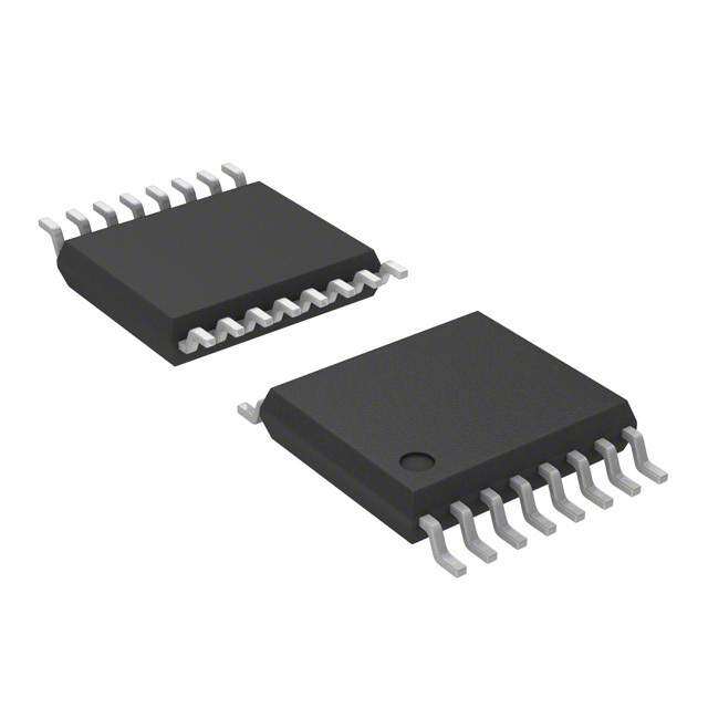
| 描述 | IC DATA SELECTOR/MUX SGL 16SOIC编码器、解码器、复用器和解复用器 QUAD 2Ln To 1Ln Data Selector Multiplexr |
| 产品分类 | |
| 品牌 | Texas Instruments |
| 产品手册 | |
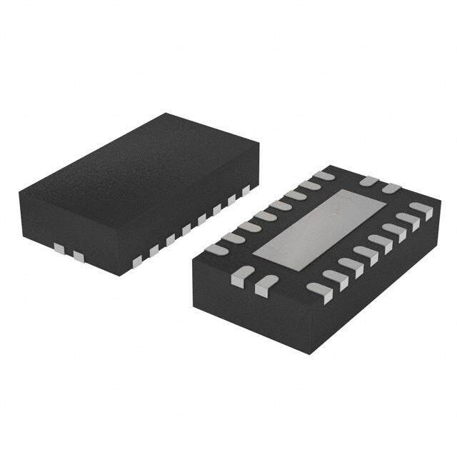
| 产品图片 |
|
| rohs | 符合RoHS无铅 / 符合限制有害物质指令(RoHS)规范要求 |
| 产品系列 | 逻辑集成电路,编码器、解码器、复用器和解复用器,Texas Instruments SN74HC257DG474HC |
| 数据手册 | |
| 产品型号 | SN74HC257DG4 |
| 产品 | Selectors / Multiplexers |
| 产品种类 | 编码器、解码器、复用器和解复用器 |
| 传播延迟时间 | 150 ns at 2 V, 30 ns at 4.5 V, 26 ns at 6 V |
| 供应商器件封装 | 16-SOIC N |
| 包装 | 管件 |
| 单位重量 | 141.700 mg |
| 商标 | Texas Instruments |
| 安装类型 | 表面贴装 |
| 安装风格 | SMD/SMT |
| 封装 | Tube |
| 封装/外壳 | 16-SOIC(0.154",3.90mm 宽) |
| 封装/箱体 | SOIC-16 |
| 工作温度 | -40°C ~ 85°C |
| 工作温度范围 | - 40 C to + 85 C |
| 工作电压 | 2 V to 6 V |
| 工厂包装数量 | 40 |
| 最大工作温度 | + 85 C |
| 最小工作温度 | - 40 C |
| 标准包装 | 40 |
| 独立电路 | 1 |
| 电压-电源 | 2 V ~ 6 V |
| 电压源 | 单电源 |
| 电流-输出高,低 | 7.8mA,7.8mA |
| 电源电压-最大 | 6 V |
| 电源电压-最小 | 2 V |
| 电路 | 4 x 2:1 |
| 类型 | 多路复用器 |
| 系列 | SN74HC257 |
| 输入/输出线数量 | 2 / 1 |
| 输入线路数量 | 2 |
| 输出线路数量 | 1 |
| 逻辑系列 | HC |


- 商务部:美国ITC正式对集成电路等产品启动337调查
- 曝三星4nm工艺存在良率问题 高通将骁龙8 Gen1或转产台积电
- 太阳诱电将投资9.5亿元在常州建新厂生产MLCC 预计2023年完工
- 英特尔发布欧洲新工厂建设计划 深化IDM 2.0 战略
- 台积电先进制程称霸业界 有大客户加持明年业绩稳了
- 达到5530亿美元!SIA预计今年全球半导体销售额将创下新高
- 英特尔拟将自动驾驶子公司Mobileye上市 估值或超500亿美元
- 三星加码芯片和SET,合并消费电子和移动部门,撤换高东真等 CEO
- 三星电子宣布重大人事变动 还合并消费电子和移动部门
- 海关总署:前11个月进口集成电路产品价值2.52万亿元 增长14.8%


PDF Datasheet 数据手册内容提取
(cid:1)(cid:2)(cid:3)(cid:4)(cid:5)(cid:6)(cid:7)(cid:8)(cid:3)(cid:9)(cid:10) (cid:1)(cid:2)(cid:9)(cid:4)(cid:5)(cid:6)(cid:7)(cid:8)(cid:3)(cid:9) (cid:11)(cid:12)(cid:13)(cid:14)(cid:15)(cid:12)(cid:16)(cid:17)(cid:18) (cid:8)(cid:19)(cid:17)(cid:20)(cid:2)(cid:18) (cid:7)(cid:21) (cid:22)(cid:19)(cid:17)(cid:20)(cid:2)(cid:18) (cid:14)(cid:13)(cid:7)(cid:13) (cid:1)(cid:18)(cid:17)(cid:18)(cid:6)(cid:7)(cid:21)(cid:15)(cid:1)(cid:23)(cid:24)(cid:12)(cid:17)(cid:7)(cid:20)(cid:16)(cid:17)(cid:18)(cid:25)(cid:18)(cid:15)(cid:1) (cid:26)(cid:20)(cid:7)(cid:5) (cid:27)(cid:19)(cid:1)(cid:7)(cid:13)(cid:7)(cid:18) (cid:21)(cid:12)(cid:7)(cid:16)(cid:12)(cid:7)(cid:1) SCLS072D − NOVEMBER 1988 − REVISED SEPTEMBER 2003 (cid:1) Operating Voltage Range of 4.5 V to 5.5 V (cid:1) Low Input Current of 1 µA Max (cid:1) (cid:1) High-Current 3-State Outputs Interface Inputs Are TTL-Voltage Compatible Directly With System Bus (cid:1) Provide Bus Interface From Multiple (cid:1) Typical tpd = 17 ns Sources in High-Performance Systems (cid:1) Low Power Consumption, 80-µA Max I (cid:1) Buffered Inputs and Outputs CC (cid:1) ±6-mA Output Drive at 5 V SN54HCT257... J PACKAGE SN54HCT257...FK PACKAGE SN74HCT257...D OR N PACKAGE (TOP VIEW) (TOP VIEW) 1AA/B NCVCCOE A/B 1 16 VCC 1A 2 15 OE 3 2 1 20 19 1B 4 18 4A 1B 3 14 4A 1Y 5 17 4B 1Y 4 13 4B NC 6 16 NC 2A 5 12 4Y 2A 7 15 4Y 2B 6 11 3A 2B 8 14 3A 2Y 7 10 3B 9 10 1112 13 GND 8 9 3Y Y D CY B 2 N N3 3 G NC − No internal connection description/ordering information The ’HCT257 devices are designed to multiplex signals from 4-bit data sources to 4-output data lines in bus-organized systems. The 3-state outputs do not load the data lines when the output-enable (OE) input is at the high logic level. To ensure the high-impedance state during power up or power down, OE should be tied to V through a pullup CC resistor; the minimum value of the resistor is determined by the current-sinking capability of the driver. ORDERING INFORMATION ORDERABLE TOP-SIDE TA PACKAGE† PART NUMBER MARKING PDIP − N Tube of 25 SN74HCT257N SN74HCT257N Tube of 40 SN74HCT257D −−4400°°CC ttoo 8855°°CC SSOOIICC −− DD Reel of 2500 SN74HCT257DR HHCCTT225577 Reel of 250 SN74HCT257DT CDIP − J Tube of 25 SNJ54HCT257J SNJ54HCT257J −−5555°°CC ttoo 112255°°CC LCCC − FK Tube of 55 SNJ54HCT257FK SNJ54HCT257FK †Package drawings, standard packing quantities, thermal data, symbolization, and PCB design guidelines are available at www.ti.com/sc/package. Please be aware that an important notice concerning availability, standard warranty, and use in critical applications of TexasInstruments semiconductor products and disclaimers thereto appears at the end of this data sheet. (cid:12)(cid:2)(cid:17)(cid:18)(cid:1)(cid:1) (cid:21)(cid:7)(cid:5)(cid:18)(cid:15)(cid:26)(cid:20)(cid:1)(cid:18) (cid:2)(cid:21)(cid:7)(cid:18)(cid:14) (cid:28)(cid:29)(cid:30)(cid:31) !"#$%&’(cid:28) #"’(cid:28)((cid:30)’(cid:31) (cid:16)(cid:15)(cid:21)(cid:14)(cid:12)(cid:6)(cid:7)(cid:20)(cid:21)(cid:2) Copyright 2003, Texas Instruments Incorporated (cid:14)(cid:13)(cid:7)(cid:13) (cid:30)’)"*%((cid:28)(cid:30)"’ #$**&’(cid:28) ((cid:31) ") +$,-(cid:30)#((cid:28)(cid:30)"’ !((cid:28)&. (cid:16)*"!$#(cid:28)(cid:31) #"’)"*% (cid:28)" (cid:31)+&#(cid:30))(cid:30)#((cid:28)(cid:30)"’(cid:31) +&* (cid:28)(cid:29)& (cid:28)&*%(cid:31) ") (cid:7)&/((cid:31) (cid:20)’(cid:31)(cid:28)*$%&’(cid:28)(cid:31) (cid:31)(cid:28)(’!(*! 0(**(’(cid:28)1. (cid:16)*"!$#(cid:28)(cid:30)"’ +*"#&(cid:31)(cid:31)(cid:30)’2 !"&(cid:31) ’"(cid:28) ’&#&(cid:31)(cid:31)(*(cid:30)-1 (cid:30)’#-$!& (cid:28)&(cid:31)(cid:28)(cid:30)’2 ") (-- +(*(%&(cid:28)&*(cid:31). POST OFFICE BOX 655303 • DALLAS, TEXAS 75265 1
(cid:1)(cid:2)(cid:3)(cid:4)(cid:5)(cid:6)(cid:7)(cid:8)(cid:3)(cid:9)(cid:10) (cid:1)(cid:2)(cid:9)(cid:4)(cid:5)(cid:6)(cid:7)(cid:8)(cid:3)(cid:9) (cid:11)(cid:12)(cid:13)(cid:14)(cid:15)(cid:12)(cid:16)(cid:17)(cid:18) (cid:8)(cid:19)(cid:17)(cid:20)(cid:2)(cid:18) (cid:7)(cid:21) (cid:22)(cid:19)(cid:17)(cid:20)(cid:2)(cid:18) (cid:14)(cid:13)(cid:7)(cid:13) (cid:1)(cid:18)(cid:17)(cid:18)(cid:6)(cid:7)(cid:21)(cid:15)(cid:1)(cid:23)(cid:24)(cid:12)(cid:17)(cid:7)(cid:20)(cid:16)(cid:17)(cid:18)(cid:25)(cid:18)(cid:15)(cid:1) (cid:26)(cid:20)(cid:7)(cid:5) (cid:27)(cid:19)(cid:1)(cid:7)(cid:13)(cid:7)(cid:18) (cid:21)(cid:12)(cid:7)(cid:16)(cid:12)(cid:7)(cid:1) SCLS072D − NOVEMBER 1988 − REVISED SEPTEMBER 2003 FUNCTION TABLE INPUTS OOUUTTPPUUTT SSEELLEECCTT DATA OOEE YY A/B A B H X X X Z L L L X L L L H X H L H X L L L H X H H logic diagram (positive logic) 15 OE 1 A/B 2 1A 4 1Y 3 1B 5 2A 7 2Y 6 2B 11 3A 9 3Y 10 3B 14 4A 12 4Y 13 4B Pin numbers shown are for the D, J, and N packages. 2 POST OFFICE BOX 655303 • DALLAS, TEXAS 75265
(cid:1)(cid:2)(cid:3)(cid:4)(cid:5)(cid:6)(cid:7)(cid:8)(cid:3)(cid:9)(cid:10) (cid:1)(cid:2)(cid:9)(cid:4)(cid:5)(cid:6)(cid:7)(cid:8)(cid:3)(cid:9) (cid:11)(cid:12)(cid:13)(cid:14)(cid:15)(cid:12)(cid:16)(cid:17)(cid:18) (cid:8)(cid:19)(cid:17)(cid:20)(cid:2)(cid:18) (cid:7)(cid:21) (cid:22)(cid:19)(cid:17)(cid:20)(cid:2)(cid:18) (cid:14)(cid:13)(cid:7)(cid:13) (cid:1)(cid:18)(cid:17)(cid:18)(cid:6)(cid:7)(cid:21)(cid:15)(cid:1)(cid:23)(cid:24)(cid:12)(cid:17)(cid:7)(cid:20)(cid:16)(cid:17)(cid:18)(cid:25)(cid:18)(cid:15)(cid:1) (cid:26)(cid:20)(cid:7)(cid:5) (cid:27)(cid:19)(cid:1)(cid:7)(cid:13)(cid:7)(cid:18) (cid:21)(cid:12)(cid:7)(cid:16)(cid:12)(cid:7)(cid:1) SCLS072D − NOVEMBER 1988 − REVISED SEPTEMBER 2003 absolute maximum ratings over operating free-air temperature range (unless otherwise noted)† Supply voltage range, V . . . . . . . . . . . . . . . . . . . . . . . . . . . . . . . . . . . . . . . . . . . . . . . . . . . . . . . . . . −0.5 V to 7 V CC Input clamp current, I (V < 0 or V > V ) (see Note 1) . . . . . . . . . . . . . . . . . . . . . . . . . . . . . . . . . . . . ±20 mA IK I I CC Output clamp current, I (V < 0 or V > V ) (see Note 1) . . . . . . . . . . . . . . . . . . . . . . . . . . . . . . . . ±20 mA OK O O CC Continuous output current, I (V = 0 to V ) . . . . . . . . . . . . . . . . . . . . . . . . . . . . . . . . . . . . . . . . . . . . . . ±35 mA O O CC Continuous current through V or GND . . . . . . . . . . . . . . . . . . . . . . . . . . . . . . . . . . . . . . . . . . . . . . . . . . . ±70 mA CC Package thermal impedance, θJA (see Note 2): D package . . . . . . . . . . . . . . . . . . . . . . . . . . . . . . . . . . . 73°C/W N package . . . . . . . . . . . . . . . . . . . . . . . . . . . . . . . . . . . 67°C/W Storage temperature range, T . . . . . . . . . . . . . . . . . . . . . . . . . . . . . . . . . . . . . . . . . . . . . . . . . . . −65°C to 150°C stg †Stresses beyond those listed under “absolute maximum ratings” may cause permanent damage to the device. These are stress ratings only, and functional operation of the device at these or any other conditions beyond those indicated under “recommended operating conditions” is not implied. Exposure to absolute-maximum-rated conditions for extended periods may affect device reliability. NOTES: 1. The input and output voltage ratings may be exceeded if the input and output current ratings are observed. 2. The package thermal impedance is calculated in accordance with JESD 51-7. recommended operating conditions (see Note 3) SN54HCT257 SN74HCT257 UUNNIITT MIN NOM MAX MIN NOM MAX VCC Supply voltage 4.5 5 5.5 4.5 5 5.5 V VIH High-level input voltage VCC = 4.5 V to 5.5 V 2 2 V VIL Low-level input voltage VCC = 4.5 V to 5.5 V 0.8 0.8 V VI Input voltage 0 VCC 0 VCC V VO Output voltage 0 VCC 0 VCC V tt Input transition (rise and fall) time 500 500 ns TA Operating free-air temperature −55 125 −40 85 °C NOTE 3: All unused inputs of the device must be held at VCC or GND to ensure proper device operation. Refer to the TI application report, Implications of Slow or Floating CMOS Inputs, literature number SCBA004. electrical characteristics over recommended operating free-air temperature range (unless otherwise noted) TA = 25°C SN54HCT257 SN74HCT257 PPAARRAAMMEETTEERR TTEESSTT CCOONNDDIITTIIOONNSS VVCCCC UUNNIITT MIN TYP MAX MIN MAX MIN MAX IOH = −20 µA 4.4 4.499 4.4 4.4 VVOOHH VVII == VVIIHH oorr VVIILL 44..55 VV VV IOH = −6 mA 3.98 4.3 3.7 3.84 IOL = 20 µA 0.001 0.1 0.1 0.1 VVOOLL VVII == VVIIHH oorr VVIILL 44..55 VV VV IOL = 6 mA 0.17 0.26 0.4 0.33 II VI = VCC or 0 5.5 V ±0.1 ±100 ±1000 ±1000 nA IOZ VO = VCC or 0, VI = VIH or VIL 5.5 V ±0.01 ±0.5 ±10 ±5 µA ICC VI = VCC or 0, IO = 0 5.5 V 8 160 80 µA One input at 0.5 V or 2.4 V, ∆ICC‡ Other inputs at 0 or VCC 5.5 V 1.4 2.4 3 2.9 mA 4.5 V Ci to 5.5 V 3 10 10* 10 pF * On products compliant to MIL-PRF-38535, this parameter is not production tested. ‡This is the increase in supply current for each input that is at one of the specified TTL voltage levels, rather than 0 V or VCC. (cid:16)(cid:15)(cid:21)(cid:14)(cid:12)(cid:6)(cid:7) (cid:16)(cid:15)(cid:18)3(cid:20)(cid:18)(cid:26) (cid:30)’)"*%((cid:28)(cid:30)"’ #"’#&*’(cid:31) +*"!$#(cid:28)(cid:31) (cid:30)’ (cid:28)(cid:29)& )"*%((cid:28)(cid:30)4& "* !&(cid:31)(cid:30)2’ +(cid:29)((cid:31)& ") !&4&-"+%&’(cid:28). (cid:6)(cid:29)(*(#(cid:28)&*(cid:30)(cid:31)(cid:28)(cid:30)# !((cid:28)( (’! "(cid:28)(cid:29)&* (cid:31)+&#(cid:30))(cid:30)#((cid:28)(cid:30)"’(cid:31) (*& !&(cid:31)(cid:30)2’ 2"(-(cid:31). (cid:7)&/((cid:31) (cid:20)’(cid:31)(cid:28)*$%&’(cid:28)(cid:31) *&(cid:31)&*4&(cid:31) (cid:28)(cid:29)& *(cid:30)2(cid:29)(cid:28) (cid:28)" #(cid:29)(’2& "* !(cid:30)(cid:31)#"’(cid:28)(cid:30)’$& (cid:28)(cid:29)&(cid:31)& +*"!$#(cid:28)(cid:31) 0(cid:30)(cid:28)(cid:29)"$(cid:28) ’"(cid:28)(cid:30)#&. POST OFFICE BOX 655303 • DALLAS, TEXAS 75265 3
(cid:1)(cid:2)(cid:3)(cid:4)(cid:5)(cid:6)(cid:7)(cid:8)(cid:3)(cid:9)(cid:10) (cid:1)(cid:2)(cid:9)(cid:4)(cid:5)(cid:6)(cid:7)(cid:8)(cid:3)(cid:9) (cid:11)(cid:12)(cid:13)(cid:14)(cid:15)(cid:12)(cid:16)(cid:17)(cid:18) (cid:8)(cid:19)(cid:17)(cid:20)(cid:2)(cid:18) (cid:7)(cid:21) (cid:22)(cid:19)(cid:17)(cid:20)(cid:2)(cid:18) (cid:14)(cid:13)(cid:7)(cid:13) (cid:1)(cid:18)(cid:17)(cid:18)(cid:6)(cid:7)(cid:21)(cid:15)(cid:1)(cid:23)(cid:24)(cid:12)(cid:17)(cid:7)(cid:20)(cid:16)(cid:17)(cid:18)(cid:25)(cid:18)(cid:15)(cid:1) (cid:26)(cid:20)(cid:7)(cid:5) (cid:27)(cid:19)(cid:1)(cid:7)(cid:13)(cid:7)(cid:18) (cid:21)(cid:12)(cid:7)(cid:16)(cid:12)(cid:7)(cid:1) SCLS072D − NOVEMBER 1988 − REVISED SEPTEMBER 2003 switching characteristics over recommended operating free-air temperature range, C = 50 pF L (unless otherwise noted) (see Figure 1) FFRROOMM TTOO TA = 25°C SN54HCT257 SN74HCT257 PPAARRAAMMEETTEERR (INPUT) (OUTPUT) VVCCCC MIN TYP MAX MIN MAX MIN MAX UUNNIITT 4.5 V 20 30 45 38 AA oorr BB YY 5.5 V 17 27 40 34 ttppdd nnss 4.5 V 20 30 45 38 AA//BB YY 5.5 V 17 27 40 34 4.5 V 20 30 45 38 tteenn OOEE YY nnss 5.5 V 17 27 40 34 4.5 V 20 30 45 38 ttddiiss OOEE YY nnss 5.5 V 17 27 40 34 4.5 V 8 15 22 19 tttt AAnnyy nnss 5.5 V 7 14 21 17 switching characteristics over recommended operating free-air temperature range, C = 150 pF L (unless otherwise noted) (see Figure 1) FFRROOMM TTOO TA = 25°C SN54HCT257 SN74HCT257 PPAARRAAMMEETTEERR (INPUT) (OUTPUT) VVCCCC MIN TYP MAX MIN MAX MIN MAX UUNNIITT 4.5 V 22 38 57 48 AA oorr BB YY 5.5 V 19 35 53 44 ttppdd nnss 4.5 V 22 38 57 48 AA//BB YY 5.5 V 19 35 53 44 4.5 V 23 40 60 50 tteenn OOEE YY nnss 5.5 V 20 38 57 48 4.5 V 17 42 63 53 tttt AAnnyy nnss 5.5 V 14 38 57 48 operating characteristics, T = 25°C A PARAMETER TEST CONDITIONS TYP UNIT Cpd Power dissipation capacitance No load 13 pF (cid:16)(cid:15)(cid:21)(cid:14)(cid:12)(cid:6)(cid:7) (cid:16)(cid:15)(cid:18)3(cid:20)(cid:18)(cid:26) (cid:30)’)"*%((cid:28)(cid:30)"’ #"’#&*’(cid:31) +*"!$#(cid:28)(cid:31) (cid:30)’ (cid:28)(cid:29)& )"*%((cid:28)(cid:30)4& "* !&(cid:31)(cid:30)2’ +(cid:29)((cid:31)& ") !&4&-"+%&’(cid:28). (cid:6)(cid:29)(*(#(cid:28)&*(cid:30)(cid:31)(cid:28)(cid:30)# !((cid:28)( (’! "(cid:28)(cid:29)&* (cid:31)+&#(cid:30))(cid:30)#((cid:28)(cid:30)"’(cid:31) (*& !&(cid:31)(cid:30)2’ 2"(-(cid:31). (cid:7)&/((cid:31) (cid:20)’(cid:31)(cid:28)*$%&’(cid:28)(cid:31) *&(cid:31)&*4&(cid:31) (cid:28)(cid:29)& *(cid:30)2(cid:29)(cid:28) (cid:28)" #(cid:29)(’2& "* !(cid:30)(cid:31)#"’(cid:28)(cid:30)’$& (cid:28)(cid:29)&(cid:31)& +*"!$#(cid:28)(cid:31) 0(cid:30)(cid:28)(cid:29)"$(cid:28) ’"(cid:28)(cid:30)#&. 4 POST OFFICE BOX 655303 • DALLAS, TEXAS 75265
(cid:1)(cid:2)(cid:3)(cid:4)(cid:5)(cid:6)(cid:7)(cid:8)(cid:3)(cid:9)(cid:10) (cid:1)(cid:2)(cid:9)(cid:4)(cid:5)(cid:6)(cid:7)(cid:8)(cid:3)(cid:9) (cid:11)(cid:12)(cid:13)(cid:14)(cid:15)(cid:12)(cid:16)(cid:17)(cid:18) (cid:8)(cid:19)(cid:17)(cid:20)(cid:2)(cid:18) (cid:7)(cid:21) (cid:22)(cid:19)(cid:17)(cid:20)(cid:2)(cid:18) (cid:14)(cid:13)(cid:7)(cid:13) (cid:1)(cid:18)(cid:17)(cid:18)(cid:6)(cid:7)(cid:21)(cid:15)(cid:1)(cid:23)(cid:24)(cid:12)(cid:17)(cid:7)(cid:20)(cid:16)(cid:17)(cid:18)(cid:25)(cid:18)(cid:15)(cid:1) (cid:26)(cid:20)(cid:7)(cid:5) (cid:27)(cid:19)(cid:1)(cid:7)(cid:13)(cid:7)(cid:18) (cid:21)(cid:12)(cid:7)(cid:16)(cid:12)(cid:7)(cid:1) SCLS072D − NOVEMBER 1988 − REVISED SEPTEMBER 2003 PARAMETER MEASUREMENT INFORMATION VCC PARAMETER RL CL S1 S2 S1 tPZH 50 pF Open Closed Test ten 1 kΩ or From Output Point RL tPZL 150 pF Closed Open Under Test tPHZ Open Closed CL tdis 1 kΩ 50 pF (see Note A) S2 tPLZ Closed Open 50 pF tpd or tt −− or Open Open 150 pF LOAD CIRCUIT 3 V Output 3 V Input 1.3 V 1.3 V Control 1.3 V 1.3 V (Low-Level 0 V Enabling) 0 V tPLH tPHL tPZL tPLZ In-Phase 90% 90% VOH Output ≈VCC Output 1.3 V 1.3 V Waveform 1 1.3 V 10% 10% tr tfVOL (See Note B) 10% VOL tPHL tPLH tPZH tPHZ Out-of- 90% 90% VOH Output VOH Phase 1.3 V 1.3 V 90% Output 10% 10% Waveform 2 1.3 V VOL (See Note B) ≈0 V tf tr VOLTAGE WAVEFORMS VOLTAGE WAVEFORMS OUTPUT AND 3-STATE BIDIRECTIONAL I/O ENABLE AND DISABLE TIMES FOR 3-STATE OUTPUTS PROPAGATION DELAY TIME NOTES: A. CL includes probe and test-fixture capacitance. B. Waveform 1 is for an output with internal conditions such that the output is low except when disabled by the output control. Waveform 2 is for an output with internal conditions such that the output is high except when disabled by the output control. C. Phase relationships between waveforms were chosen arbitrarily. All input pulses are supplied by generators having the following characteristics: PRR ≤ 1 MHz, ZO = 50 Ω, tr = 6 ns, tf = 6 ns. D. The outputs are measured one at a time with one input transition per measurement. E. tPLZ and tPHZ are the same as tdis. F. tPZL and tPZH are the same as ten. G. tPLH and tPHL are the same as tpd. Figure 1. Load Circuit and Voltage Waveforms POST OFFICE BOX 655303 • DALLAS, TEXAS 75265 5
PACKAGE OPTION ADDENDUM www.ti.com 24-Aug-2018 PACKAGING INFORMATION Orderable Device Status Package Type Package Pins Package Eco Plan Lead/Ball Finish MSL Peak Temp Op Temp (°C) Device Marking Samples (1) Drawing Qty (2) (6) (3) (4/5) SN74HCT257D ACTIVE SOIC D 16 40 Green (RoHS CU NIPDAU Level-1-260C-UNLIM -40 to 85 HCT257 & no Sb/Br) SN74HCT257DR ACTIVE SOIC D 16 2500 Green (RoHS CU NIPDAU Level-1-260C-UNLIM -40 to 85 HCT257 & no Sb/Br) SN74HCT257DRE4 ACTIVE SOIC D 16 2500 Green (RoHS CU NIPDAU Level-1-260C-UNLIM -40 to 85 HCT257 & no Sb/Br) SN74HCT257N ACTIVE PDIP N 16 25 Green (RoHS CU NIPDAU N / A for Pkg Type -40 to 85 SN74HCT257N & no Sb/Br) (1) The marketing status values are defined as follows: ACTIVE: Product device recommended for new designs. LIFEBUY: TI has announced that the device will be discontinued, and a lifetime-buy period is in effect. NRND: Not recommended for new designs. Device is in production to support existing customers, but TI does not recommend using this part in a new design. PREVIEW: Device has been announced but is not in production. Samples may or may not be available. OBSOLETE: TI has discontinued the production of the device. (2) RoHS: TI defines "RoHS" to mean semiconductor products that are compliant with the current EU RoHS requirements for all 10 RoHS substances, including the requirement that RoHS substance do not exceed 0.1% by weight in homogeneous materials. Where designed to be soldered at high temperatures, "RoHS" products are suitable for use in specified lead-free processes. TI may reference these types of products as "Pb-Free". RoHS Exempt: TI defines "RoHS Exempt" to mean products that contain lead but are compliant with EU RoHS pursuant to a specific EU RoHS exemption. Green: TI defines "Green" to mean the content of Chlorine (Cl) and Bromine (Br) based flame retardants meet JS709B low halogen requirements of <=1000ppm threshold. Antimony trioxide based flame retardants must also meet the <=1000ppm threshold requirement. (3) MSL, Peak Temp. - The Moisture Sensitivity Level rating according to the JEDEC industry standard classifications, and peak solder temperature. (4) There may be additional marking, which relates to the logo, the lot trace code information, or the environmental category on the device. (5) Multiple Device Markings will be inside parentheses. Only one Device Marking contained in parentheses and separated by a "~" will appear on a device. If a line is indented then it is a continuation of the previous line and the two combined represent the entire Device Marking for that device. (6) Lead/Ball Finish - Orderable Devices may have multiple material finish options. Finish options are separated by a vertical ruled line. Lead/Ball Finish values may wrap to two lines if the finish value exceeds the maximum column width. Important Information and Disclaimer:The information provided on this page represents TI's knowledge and belief as of the date that it is provided. TI bases its knowledge and belief on information provided by third parties, and makes no representation or warranty as to the accuracy of such information. Efforts are underway to better integrate information from third parties. TI has taken and Addendum-Page 1
PACKAGE OPTION ADDENDUM www.ti.com 24-Aug-2018 continues to take reasonable steps to provide representative and accurate information but may not have conducted destructive testing or chemical analysis on incoming materials and chemicals. TI and TI suppliers consider certain information to be proprietary, and thus CAS numbers and other limited information may not be available for release. In no event shall TI's liability arising out of such information exceed the total purchase price of the TI part(s) at issue in this document sold by TI to Customer on an annual basis. Addendum-Page 2
PACKAGE MATERIALS INFORMATION www.ti.com 19-Mar-2008 TAPE AND REEL INFORMATION *Alldimensionsarenominal Device Package Package Pins SPQ Reel Reel A0(mm) B0(mm) K0(mm) P1 W Pin1 Type Drawing Diameter Width (mm) (mm) Quadrant (mm) W1(mm) SN74HCT257DR SOIC D 16 2500 330.0 16.4 6.5 10.3 2.1 8.0 16.0 Q1 PackMaterials-Page1
PACKAGE MATERIALS INFORMATION www.ti.com 19-Mar-2008 *Alldimensionsarenominal Device PackageType PackageDrawing Pins SPQ Length(mm) Width(mm) Height(mm) SN74HCT257DR SOIC D 16 2500 333.2 345.9 28.6 PackMaterials-Page2
None
None
None
IMPORTANTNOTICE TexasInstrumentsIncorporated(TI)reservestherighttomakecorrections,enhancements,improvementsandotherchangestoits semiconductorproductsandservicesperJESD46,latestissue,andtodiscontinueanyproductorserviceperJESD48,latestissue.Buyers shouldobtainthelatestrelevantinformationbeforeplacingordersandshouldverifythatsuchinformationiscurrentandcomplete. TI’spublishedtermsofsaleforsemiconductorproducts(http://www.ti.com/sc/docs/stdterms.htm)applytothesaleofpackagedintegrated circuitproductsthatTIhasqualifiedandreleasedtomarket.AdditionaltermsmayapplytotheuseorsaleofothertypesofTIproductsand services. ReproductionofsignificantportionsofTIinformationinTIdatasheetsispermissibleonlyifreproductioniswithoutalterationandis accompaniedbyallassociatedwarranties,conditions,limitations,andnotices.TIisnotresponsibleorliableforsuchreproduced documentation.Informationofthirdpartiesmaybesubjecttoadditionalrestrictions.ResaleofTIproductsorserviceswithstatements differentfromorbeyondtheparametersstatedbyTIforthatproductorservicevoidsallexpressandanyimpliedwarrantiesforthe associatedTIproductorserviceandisanunfairanddeceptivebusinesspractice.TIisnotresponsibleorliableforanysuchstatements. BuyersandotherswhoaredevelopingsystemsthatincorporateTIproducts(collectively,“Designers”)understandandagreethatDesigners remainresponsibleforusingtheirindependentanalysis,evaluationandjudgmentindesigningtheirapplicationsandthatDesignershave fullandexclusiveresponsibilitytoassurethesafetyofDesigners'applicationsandcomplianceoftheirapplications(andofallTIproducts usedinorforDesigners’applications)withallapplicableregulations,lawsandotherapplicablerequirements.Designerrepresentsthat,with respecttotheirapplications,Designerhasallthenecessaryexpertisetocreateandimplementsafeguardsthat(1)anticipatedangerous consequencesoffailures,(2)monitorfailuresandtheirconsequences,and(3)lessenthelikelihoodoffailuresthatmightcauseharmand takeappropriateactions.DesigneragreesthatpriortousingordistributinganyapplicationsthatincludeTIproducts,Designerwill thoroughlytestsuchapplicationsandthefunctionalityofsuchTIproductsasusedinsuchapplications. TI’sprovisionoftechnical,applicationorotherdesignadvice,qualitycharacterization,reliabilitydataorotherservicesorinformation, including,butnotlimitedto,referencedesignsandmaterialsrelatingtoevaluationmodules,(collectively,“TIResources”)areintendedto assistdesignerswhoaredevelopingapplicationsthatincorporateTIproducts;bydownloading,accessingorusingTIResourcesinany way,Designer(individuallyor,ifDesignerisactingonbehalfofacompany,Designer’scompany)agreestouseanyparticularTIResource solelyforthispurposeandsubjecttothetermsofthisNotice. TI’sprovisionofTIResourcesdoesnotexpandorotherwisealterTI’sapplicablepublishedwarrantiesorwarrantydisclaimersforTI products,andnoadditionalobligationsorliabilitiesarisefromTIprovidingsuchTIResources.TIreservestherighttomakecorrections, enhancements,improvementsandotherchangestoitsTIResources.TIhasnotconductedanytestingotherthanthatspecifically describedinthepublisheddocumentationforaparticularTIResource. Designerisauthorizedtouse,copyandmodifyanyindividualTIResourceonlyinconnectionwiththedevelopmentofapplicationsthat includetheTIproduct(s)identifiedinsuchTIResource.NOOTHERLICENSE,EXPRESSORIMPLIED,BYESTOPPELOROTHERWISE TOANYOTHERTIINTELLECTUALPROPERTYRIGHT,ANDNOLICENSETOANYTECHNOLOGYORINTELLECTUALPROPERTY RIGHTOFTIORANYTHIRDPARTYISGRANTEDHEREIN,includingbutnotlimitedtoanypatentright,copyright,maskworkright,or otherintellectualpropertyrightrelatingtoanycombination,machine,orprocessinwhichTIproductsorservicesareused.Information regardingorreferencingthird-partyproductsorservicesdoesnotconstitutealicensetousesuchproductsorservices,orawarrantyor endorsementthereof.UseofTIResourcesmayrequirealicensefromathirdpartyunderthepatentsorotherintellectualpropertyofthe thirdparty,oralicensefromTIunderthepatentsorotherintellectualpropertyofTI. TIRESOURCESAREPROVIDED“ASIS”ANDWITHALLFAULTS.TIDISCLAIMSALLOTHERWARRANTIESOR REPRESENTATIONS,EXPRESSORIMPLIED,REGARDINGRESOURCESORUSETHEREOF,INCLUDINGBUTNOTLIMITEDTO ACCURACYORCOMPLETENESS,TITLE,ANYEPIDEMICFAILUREWARRANTYANDANYIMPLIEDWARRANTIESOF MERCHANTABILITY,FITNESSFORAPARTICULARPURPOSE,ANDNON-INFRINGEMENTOFANYTHIRDPARTYINTELLECTUAL PROPERTYRIGHTS.TISHALLNOTBELIABLEFORANDSHALLNOTDEFENDORINDEMNIFYDESIGNERAGAINSTANYCLAIM, INCLUDINGBUTNOTLIMITEDTOANYINFRINGEMENTCLAIMTHATRELATESTOORISBASEDONANYCOMBINATIONOF PRODUCTSEVENIFDESCRIBEDINTIRESOURCESOROTHERWISE.INNOEVENTSHALLTIBELIABLEFORANYACTUAL, DIRECT,SPECIAL,COLLATERAL,INDIRECT,PUNITIVE,INCIDENTAL,CONSEQUENTIALOREXEMPLARYDAMAGESIN CONNECTIONWITHORARISINGOUTOFTIRESOURCESORUSETHEREOF,ANDREGARDLESSOFWHETHERTIHASBEEN ADVISEDOFTHEPOSSIBILITYOFSUCHDAMAGES. UnlessTIhasexplicitlydesignatedanindividualproductasmeetingtherequirementsofaparticularindustrystandard(e.g.,ISO/TS16949 andISO26262),TIisnotresponsibleforanyfailuretomeetsuchindustrystandardrequirements. WhereTIspecificallypromotesproductsasfacilitatingfunctionalsafetyorascompliantwithindustryfunctionalsafetystandards,such productsareintendedtohelpenablecustomerstodesignandcreatetheirownapplicationsthatmeetapplicablefunctionalsafetystandards andrequirements.Usingproductsinanapplicationdoesnotbyitselfestablishanysafetyfeaturesintheapplication.Designersmust ensurecompliancewithsafety-relatedrequirementsandstandardsapplicabletotheirapplications.DesignermaynotuseanyTIproductsin life-criticalmedicalequipmentunlessauthorizedofficersofthepartieshaveexecutedaspecialcontractspecificallygoverningsuchuse. Life-criticalmedicalequipmentismedicalequipmentwherefailureofsuchequipmentwouldcauseseriousbodilyinjuryordeath(e.g.,life support,pacemakers,defibrillators,heartpumps,neurostimulators,andimplantables).Suchequipmentincludes,withoutlimitation,all medicaldevicesidentifiedbytheU.S.FoodandDrugAdministrationasClassIIIdevicesandequivalentclassificationsoutsidetheU.S. TImayexpresslydesignatecertainproductsascompletingaparticularqualification(e.g.,Q100,MilitaryGrade,orEnhancedProduct). Designersagreethatithasthenecessaryexpertisetoselecttheproductwiththeappropriatequalificationdesignationfortheirapplications andthatproperproductselectionisatDesigners’ownrisk.Designersaresolelyresponsibleforcompliancewithalllegalandregulatory requirementsinconnectionwithsuchselection. DesignerwillfullyindemnifyTIanditsrepresentativesagainstanydamages,costs,losses,and/orliabilitiesarisingoutofDesigner’snon- compliancewiththetermsandprovisionsofthisNotice. MailingAddress:TexasInstruments,PostOfficeBox655303,Dallas,Texas75265 Copyright©2018,TexasInstrumentsIncorporated