ICGOO在线商城 > 集成电路(IC) > 逻辑 - 栅极和逆变器 > SN74HC05N
 Datasheet下载
- 型号: SN74HC05N
- 制造商: Texas Instruments
- 库位|库存: xxxx|xxxx
- 要求:
| 数量阶梯 | 香港交货 | 国内含税 |
| +xxxx | $xxxx | ¥xxxx |
查看当月历史价格
查看今年历史价格
SN74HC05N产品简介:
ICGOO电子元器件商城为您提供SN74HC05N由Texas Instruments设计生产,在icgoo商城现货销售,并且可以通过原厂、代理商等渠道进行代购。 SN74HC05N价格参考¥1.15-¥3.28。Texas InstrumentsSN74HC05N封装/规格:逻辑 - 栅极和逆变器, Inverter IC 6 Channel Open Drain 14-PDIP。您可以下载SN74HC05N参考资料、Datasheet数据手册功能说明书,资料中有SN74HC05N 详细功能的应用电路图电压和使用方法及教程。
SN74HC05N 是由德州仪器(Texas Instruments)生产的逻辑电路器件,属于“逻辑 - 栅极和逆变器”类别。它是一个六通道的非门(逆变器),具有高电平转换功能,能够将TTL(晶体管-晶体管逻辑)电平转换为CMOS(互补金属氧化物半导体)电平。

 应用场景:

1. 信号反相:
   SN74HC05N 最常见的应用场景是用于信号反相。在数字电路中,有时需要将一个高电平信号转换为低电平信号,或者反之亦然。通过使用SN74HC05N,可以轻松实现这一功能。例如,在控制电路中,当需要对某个输入信号进行反相处理时,可以直接使用该芯片中的非门来实现。

2. 电平转换:
   该芯片还支持从TTL电平到CMOS电平的转换。在混合信号系统中,不同的逻辑系列可能有不同的电压标准。SN74HC05N 可以确保信号在不同逻辑电平之间的正确传输,避免因电平不匹配导致的误触发或损坏。

3. 驱动能力增强:
   SN74HC05N 具有较高的输出驱动能力,适用于需要驱动多个负载的情况。例如,在多路复用器、解码器等复杂电路中,单个信号源可能需要同时驱动多个输入端口。此时,SN74HC05N 可以提供足够的电流驱动能力,确保信号的稳定性和完整性。

4. 时钟信号生成与处理:
   在时钟电路中,SN74HC05N 可用于生成或处理时钟信号。例如,某些应用中需要对时钟信号进行反相处理,以实现同步或异步操作。此外,它还可以用于产生分频后的时钟信号,通过与其他逻辑器件配合,构建复杂的时钟分配网络。

5. 数据通信与接口设计:
   在数据通信和接口设计中,SN74HC05N 可以用于信号调理和反相。例如,在串行通信协议(如UART、SPI、I2C)中,有时需要对信号进行反相处理,以满足特定的通信标准或硬件要求。

6. 音频信号处理:
   虽然主要用于数字电路,但在某些音频应用中,SN74HC05N 也可以用于简单的信号反相或电平转换,尤其是在涉及到数字音频信号处理的场合。

总之,SN74HC05N 作为一种通用的非门器件,广泛应用于各种数字电路中,特别适合于需要信号反相、电平转换和驱动能力增强的场合。
| 参数 | 数值 |
| 产品目录 | 集成电路 (IC)半导体 |
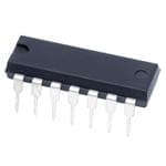
| 描述 | IC HEX INVERTER W/OD 14-DIP缓冲器和线路驱动器 Hex w/ OD |
| 产品分类 | |
| 品牌 | Texas Instruments |
| 产品手册 | |
| 产品图片 |
|
| rohs | 符合RoHS无铅 / 符合限制有害物质指令(RoHS)规范要求 |
| 产品系列 | 逻辑集成电路,缓冲器和线路驱动器,Texas Instruments SN74HC05N74HC |
| 数据手册 | |
| 产品型号 | SN74HC05N |
| PCN设计/规格 | |
| 不同V、最大CL时的最大传播延迟 | 20ns @ 6V,50pF |
| 产品目录页面 | |
| 产品种类 | 缓冲器和线路驱动器 |
| 传播延迟时间 | 115 ns at 2 V, 23 ns at 4.5 V, 20 ns at 6 V |
| 低电平输出电流 | 5.2 mA |
| 供应商器件封装 | 14-PDIP |
| 其它名称 | 296-1568 |
| 包装 | 管件 |
| 单位重量 | 1 g |
| 商标 | Texas Instruments |
| 安装类型 | 通孔 |
| 安装风格 | Through Hole |
| 封装 | Tube |
| 封装/外壳 | 14-DIP(0.300",7.62mm) |
| 封装/箱体 | PDIP-14 |
| 工作温度 | -40°C ~ 85°C |
| 工厂包装数量 | 25 |
| 最大工作温度 | + 85 C |
| 最小工作温度 | - 40 C |
| 极性 | Inverting |
| 标准包装 | 25 |
| 每芯片的通道数量 | 5 |
| 特性 | 开路漏极 |
| 电压-电源 | 2 V ~ 6 V |
| 电流-输出高,低 | -,5.2mA |
| 电流-静态(最大值) | 2µA |
| 电源电压-最大 | 6 V |
| 电源电压-最小 | 2 V |
| 电源电流 | 0.02 mA |
| 电路数 | 6 |
| 系列 | SN74HC05 |
| 输入数 | 6 |
| 输入线路数量 | 6 |
| 输出类型 | Open Drain |
| 输出线路数量 | 6 |
| 逻辑电平-低 | 0.5 V ~ 1.8 V |
| 逻辑电平-高 | 1.5 V ~ 4.2 V |
| 逻辑类型 | |
| 逻辑系列 | HC |
| 高电平输出电流 | - 0.005 mA |


- 商务部:美国ITC正式对集成电路等产品启动337调查
- 曝三星4nm工艺存在良率问题 高通将骁龙8 Gen1或转产台积电
- 太阳诱电将投资9.5亿元在常州建新厂生产MLCC 预计2023年完工
- 英特尔发布欧洲新工厂建设计划 深化IDM 2.0 战略
- 台积电先进制程称霸业界 有大客户加持明年业绩稳了
- 达到5530亿美元!SIA预计今年全球半导体销售额将创下新高
- 英特尔拟将自动驾驶子公司Mobileye上市 估值或超500亿美元
- 三星加码芯片和SET,合并消费电子和移动部门,撤换高东真等 CEO
- 三星电子宣布重大人事变动 还合并消费电子和移动部门
- 海关总署:前11个月进口集成电路产品价值2.52万亿元 增长14.8%


PDF Datasheet 数据手册内容提取
Product Sample & Technical Tools & Support & Folder Buy Documents Software Community SN54HC05,SN74HC05 SCLS080E–FEBRUARY2015–REVISEDMARCH2015 SNx4HC05 Hex Inverters With Open-Drain Outputs 1 Features 3 Description • WideOperatingVoltageRangeof2Vto6V The SNx4HC05 devices contain six independent 1 inverters. They perform the Boolean function Y = A in • OutputscanDriveupto10LSTTLLoads positive logic. The open-drain outputs require pullup • Low-PowerConsumption,20-μAMaximumICC resistors to perform correctly. They may be • Typicalt =8ns connected to other open-drain outputs to implement pd active-low wired-OR or active-high wired-AND • ±4-mAOutputDriveat5V functions. • LowInputCurrentof1-μAMaximum DeviceInformation(1) 2 Applications PARTNUMBER PACKAGE BODYSIZE(NOM) • Mice PDIP(14) 19.30mm×6.40mm • Printers SOIC(14) 8.65mm×3.91mm SN74HC05 • ACInverterDrives SOP(14) 10.30mm×5.30mm • UPS TSSOP(14) 5.00mm×4.40mm • ACServoDrives (1) For all available packages, see the orderable addendum at theendofthedatasheet. • OtherMotorDrives space space space LogicDiagram(PositiveLogic) A Y 1 An IMPORTANT NOTICE at the end of this data sheet addresses availability, warranty, changes, use in safety-critical applications, intellectualpropertymattersandotherimportantdisclaimers.PRODUCTIONDATA.
SN54HC05,SN74HC05 SCLS080E–FEBRUARY2015–REVISEDMARCH2015 www.ti.com Table of Contents 1 Features.................................................................. 1 8.2 FunctionalBlockDiagram.........................................7 2 Applications........................................................... 1 8.3 FeatureDescription...................................................7 3 Description............................................................. 1 8.4 DeviceFunctionalModes..........................................7 4 RevisionHistory..................................................... 2 9 ApplicationandImplementation.......................... 8 9.1 ApplicationInformation..............................................8 5 PinConfigurationandFunctions......................... 3 9.2 TypicalApplication ...................................................8 6 Specifications......................................................... 4 10 PowerSupplyRecommendations....................... 9 6.1 AbsoluteMaximumRatings......................................4 11 Layout..................................................................... 9 6.2 ESDRatings..............................................................4 6.3 RecommendedOperatingConditions.......................4 11.1 LayoutGuidelines...................................................9 6.4 ThermalInformation..................................................5 11.2 LayoutExample......................................................9 6.5 ElectricalCharacteristics...........................................5 12 DeviceandDocumentationSupport................. 10 6.6 SwitchingCharacteristics..........................................5 12.1 DocumentationSupport........................................10 6.7 OperatingCharacteristics..........................................5 12.2 RelatedLinks........................................................10 6.8 TypicalCharacteristics..............................................6 12.3 Trademarks...........................................................10 7 ParameterMeasurementInformation..................6 12.4 ElectrostaticDischargeCaution............................10 12.5 Glossary................................................................10 8 DetailedDescription.............................................. 7 13 Mechanical,Packaging,andOrderable 8.1 Overview...................................................................7 Information........................................................... 10 4 Revision History ChangesfromRevisionD(August2003)toRevisionE Page • AddedPinConfigurationandFunctionssection,ESDRatingstable,FeatureDescriptionsection,DeviceFunctional Modes,ApplicationandImplementationsection,PowerSupplyRecommendationssection,Layoutsection,Device andDocumentationSupportsection,andMechanical,Packaging,andOrderableInformationsection .............................. 1 2 SubmitDocumentationFeedback Copyright©2015,TexasInstrumentsIncorporated ProductFolderLinks:SN54HC05 SN74HC05
SN54HC05,SN74HC05 www.ti.com SCLS080E–FEBRUARY2015–REVISEDMARCH2015 5 Pin Configuration and Functions SN74HC05:D,N,NS,orPWPackage,14-PinSOIC,PDIP,SOP, orTSSOP SN54HC05:FKPackage SN54HC05:JorWPackage,19-PinCDIPorCFP 20-PinLCCC (TopView) (TopView) C Y A C CA 1A 1 14 VCC 1 1 N V 6 1Y 2 13 6A 3 2 1 20 19 2A 3 12 6Y 2A 4 18 6Y 2Y 4 11 5A NC 5 17 NC 3A 5 10 5Y 2Y 6 16 5A 3Y 6 9 4A NC 7 15 NC GND 7 8 4Y 3A 8 14 5Y 9 10 1112 13 YD CY A 3N N4 4 G NC–Nointernalconnection PinFunctions PIN I/O DESCRIPTION NAME NO. LCCCNO. 1A 1 2 I Input1 1Y 2 3 O Output1 2A 3 4 I Input2 2Y 4 6 O Output2 3A 5 8 I Input3 3Y 6 9 O Output3 GND 7 10 – Groundpin 4A 9 13 I Input4 4Y 8 12 O Output4 5A 11 16 I Input5 5Y 10 14 O Output5 6A 13 19 I Input6 6Y 12 18 O Output6 1,5,7,11, NC – – Noconnect 15,17 V 14 20 – Powerpin CC Copyright©2015,TexasInstrumentsIncorporated SubmitDocumentationFeedback 3 ProductFolderLinks:SN54HC05 SN74HC05
SN54HC05,SN74HC05 SCLS080E–FEBRUARY2015–REVISEDMARCH2015 www.ti.com 6 Specifications 6.1 Absolute Maximum Ratings overoperatingfree-airtemperaturerange(unlessotherwisenoted) (1) MIN MAX UNIT V Supplyvoltage –0.5 7 V CC I Inputclampcurrent,V <0orV >V (2) –20 20 mA IK I I CC I Outputclampcurrent,V <0orV >V (2) –20 20 mA OK O O CC I Continuousoutputcurrent,V =0toV –25 25 mA O O CC ContinuouscurrentthroughV orGND –50 50 mA CC T Storagetemperature –65 150 °C stg (1) StressesbeyondthoselistedunderAbsoluteMaximumRatingsmaycausepermanentdamagetothedevice.Thesearestressratings only,whichdonotimplyfunctionaloperationofthedeviceattheseoranyotherconditionsbeyondthoseindicatedunderRecommended OperatingConditions.Exposuretoabsolute-maximum-ratedconditionsforextendedperiodsmayaffectdevicereliability. (2) Theinputandoutputvoltageratingsmaybeexceedediftheinputandoutputcurrentratingsareobserved. 6.2 ESD Ratings VALUE UNIT V Electrostatic Humanbodymodel(HBM),perANSI/ESDA/JEDECJS-001(1) ±1000 V (ESD) discharge (1) JEDECdocumentJEP155statesthat500-VHBMallowssafemanufacturingwithastandardESDcontrolprocess. 6.3 Recommended Operating Conditions See (1) MIN NOM MAX UNIT V Supplyvoltage 2 5 6 V CC V =2V 1.5 CC V High-levelinputvoltage V =4.5V 3.15 V IH CC V =6V 4.2 CC V =2V 0.5 CC V Low-levelinputvoltage V =4.5V 1.35 V IL CC V =6V 1.8 CC V Inputvoltage 0 V V I CC V Outputvoltage 0 V V O CC V =2V 1000 CC Δt/Δv Inputtransitionriseorfalltime V =4.5V 500 ns CC V =6V 400 CC SN54HC05 –55 125 T Operatingfree-airtemperature °C A SN74HC05 –40 125 (1) AllunusedinputsofthedevicemustbeheldatV orGNDtoensureproperdeviceoperation.RefertotheTIapplicationreport, CC ImplicationsofSloworFloatingCMOSInputs,SCBA004. 4 SubmitDocumentationFeedback Copyright©2015,TexasInstrumentsIncorporated ProductFolderLinks:SN54HC05 SN74HC05
SN54HC05,SN74HC05 www.ti.com SCLS080E–FEBRUARY2015–REVISEDMARCH2015 6.4 Thermal Information SN74HC05 THERMALMETRIC(1) D(SOIC) N(PDIP) NS(SOP) PW(TSSOP) UNIT 14PINS 14PINS 14PINS 14PINS R Junction-to-ambientthermalresistance 89.1 85.9 86.4 117.1 θJA R Junction-to-case(top)thermalresistance 50.6 43.8 42.4 46.1 θJC(top) R Junction-to-boardthermalresistance 43.3 44.6 45.1 58.7 °C/W θJB ψ Junction-to-topcharacterizationparameter 16.3 12 11.8 4.8 JT ψ Junction-to-boardcharacterizationparameter 43 44.2 44.7 58.1 JB (1) Formoreinformationabouttraditionalandnewthermalmetrics,seetheICPackageThermalMetricsapplicationreport,SPRA953. 6.5 Electrical Characteristics overrecommendedoperatingfree-airtemperaturerange(unlessotherwisenoted) SN74HC05 SN74HC05 PARAMETER TESTCONDITIONS VCC TA=25°C SN54HC05 –40°Cto85°C –40°Cto125°C UNIT MIN TYP MAX MIN MAX MIN MAX MIN MAX IOH VI=VIHorVIL,VO=VCC 6V 0.01 0.5 10 5 5 µA 2V 0.002 0.1 0.1 0.1 0.1 IOL=20µA 4.5V 0.001 0.1 0.1 0.1 0.1 VOL VVIIL=VIHor 6V 0.001 0.1 0.1 0.1 0.1 V IOL=4mA 4.5V 0.17 0.26 0.4 0.33 0.33 IOL=5.2mA 6V 0.15 0.26 0.4 0.33 0.33 II VI=VCCor0 6V ±0.1 ±100 ±1000 ±1000 ±1000 nA ICC VI=VCCor0,IO=0 6V 2 40 20 20 µA Ci 2to6V 3 10 10 10 10 pF 6.6 Switching Characteristics overrecommendedoperatingfree-airtemperaturerange,C =50pF(unlessotherwisenoted)(seeFigure3) L SN74HC05 SN74HC05 PARAMETER FROM TO VCC TA=25°C SN54HC05 –40°Cto85°C –40°Cto125°C UNIT (INPUT) (OUTPUT) MIN TYP MAX MIN MAX MIN MAX MIN MAX 2V 60 115 175 145 160 tPLH A Y 4.5V 13 23 35 29 31 6V 10 20 30 25 28 2V 45 85 130 105 120 tPHL A Y 4.5V 9 17 26 21 23 ns 6V 8 14 22 18 21 2V 38 75 110 95 110 tf Y 4.5V 8 15 22 19 22 6V 6 13 19 16 19 6.7 Operating Characteristics T =25°C A PARAMETER TESTCONDITIONS TYP UNIT C Powerdissipationcapacitanceperinverter Noload 20 pF pd Copyright©2015,TexasInstrumentsIncorporated SubmitDocumentationFeedback 5 ProductFolderLinks:SN54HC05 SN74HC05
SN54HC05,SN74HC05 SCLS080E–FEBRUARY2015–REVISEDMARCH2015 www.ti.com 6.8 Typical Characteristics 14.5 70 60 14 50 13.5 s) s) 40 n n D ( 13 D ( P P 30 T T 12.5 20 12 10 11.5 0 -100 -50 0 50 100 150 0 2 4 6 8 Temperature D001 VCC D002 Figure1.TPDvs.Temperatureat4.5V,25°C Figure2.TPDvs.V at25°C CC 7 Parameter Measurement Information VCC RL=1kΩ FromOutput Test VCC Input 50% 50% UnderTest Point 0V CL=50pF (seeNoteA) tPLH tPHL In-Phase VOH 90% Output 50% LOADCIRCUIT 10% 10%VOL tf VCC tPHL tPLH Input 105%0% 90% 90% 501%0% Out-of-Phase 90% 50% VOH 0V Output 10% 10% tr tf tf VOL VOLTAGEWAVEFORM VOLTAGEWAVEFORMS INPUTRISEANDFALLTIMES PROPAGATIONDELAYANDOUTPUTTRANSITIONTIMES A. C includesprobeandtest-fixturecapacitance. L B. Phase relationships between waveforms were chosen arbitrarily. All input pulses are supplied by generators having thefollowingcharacteristics:PRR≤1MHz,Z =50Ω,t =6ns,t =6ns. O r f C. Theoutputsaremeasuredoneatatimewithoneinputtransitionpermeasurement. Figure3. LoadCircuitandVoltageWaveforms 6 SubmitDocumentationFeedback Copyright©2015,TexasInstrumentsIncorporated ProductFolderLinks:SN54HC05 SN74HC05
SN54HC05,SN74HC05 www.ti.com SCLS080E–FEBRUARY2015–REVISEDMARCH2015 8 Detailed Description 8.1 Overview The SNx4HC05 devices contain six independent inverters. They perform the Boolean function Y = A in positive logic.Theopen-drainoutputsrequirepullupresistorstoperformcorrectly.Theymaybeconnectedtootheropen- drainoutputstoimplementactive-lowwired-ORoractive-highwired-ANDfunctions. 8.2 Functional Block Diagram A Y Figure4. LogicDiagram(PositiveLogic) 8.3 Feature Description The device’s wide operating range allows it to be used in a variety of systems that use different logic levels. The strong current-sinking outputs allow the device to drive medium loads without significant increases in output voltage. In addition, the low power consumption makes this device a good choice for portable and battery power- sensitiveapplications. 8.4 Device Functional Modes Table1.FunctionTable (EachInverter) INPUTA OUTPUTY H L L H Copyright©2015,TexasInstrumentsIncorporated SubmitDocumentationFeedback 7 ProductFolderLinks:SN54HC05 SN74HC05
SN54HC05,SN74HC05 SCLS080E–FEBRUARY2015–REVISEDMARCH2015 www.ti.com 9 Application and Implementation NOTE Information in the following applications sections is not part of the TI component specification, and TI does not warrant its accuracy or completeness. TI’s customers are responsible for determining suitability of components for their purposes. Customers should validateandtesttheirdesignimplementationtoconfirmsystemfunctionality. 9.1 Application Information The SN74HC05 device is a low drive open-drain CMOS device that can be used for a multitude of buffer type functions. The open-drain output can be pulled to any voltage between GND and V making them Ideal for CC downtranslation. 9.2 Typical Application Buffer Function Basic LED Driver VPU VPU Wired OR uC or Logic uC or Logic uC or Logic HC05 HC05 uC or Logic HC05 Figure5. SimplifiedApplicationSchematic 9.2.1 DesignRequirements This device uses CMOS technology and is open-drain so it has low-output drive only. Take care to avoid bus contention because it can drive currents that would exceed maximum limits. Parallel output drive can create fast edgesintolightloadssoconsiderroutingandloadconditionstopreventringing. 9.2.2 DetailedDesignProcedure • Recommendedinputconditions: – Risetimeandfalltimespecssee(Δt/ΔV)inRecommendedOperatingConditions. – Specifiedhighandlowlevels.See(V andV )inRecommendedOperatingConditions. IH IL • Recommendedoutputconditions: – Loadcurrentsshouldnotexceed25mAperoutputand50mAtotalforthepart. 8 SubmitDocumentationFeedback Copyright©2015,TexasInstrumentsIncorporated ProductFolderLinks:SN54HC05 SN74HC05
SN54HC05,SN74HC05 www.ti.com SCLS080E–FEBRUARY2015–REVISEDMARCH2015 Typical Application (continued) 9.2.3 ApplicationCurve 2 1.5 V) ( 1 VIL 0.5 0 0 1 2 3 4 5 6 7 VCC(V) D001 Figure6. MaxV vs.V Level IL CC 10 Power Supply Recommendations The power supply can be any voltage between the minimum and maximum supply voltage rating located in the Recommended Operating Conditions. Each V terminal should have a good bypass capacitor to prevent power CC disturbance. For devices with a single supply, TI recommends a 0.1-µF capacitor. If there are multiple VCC terminals, then TI recommends a 0.01-µF or 0.022-µF capacitor for each power terminal. Multiple bypass capacitors can be paralleled to reject different frequencies of noise. Frequencies of 0.1 μF and 1 μF are commonly used in parallel. The bypass capacitor should be installed as close as possible to the power terminal forbestresults. 11 Layout 11.1 Layout Guidelines When using multiple bit logic devices, inputs should never float. In many cases, functions or parts of functions of digital logic devices are unused, for example, when only two inputs of a triple-input AND gate are used or only three of the four buffer gates are used. Such input pins should not be left unconnected because the undefined voltages at the outside connections result in undefined operational states. All unused inputs of digital logic devices must be connected to a high or low bias to prevent them from floating. The logic level that should be applied to any particular unused input depends on the function of the device. Generally they will be tied to GND or V whichever makes more sense or is more convenient. Floating outputs is generally acceptable, unless the CC partisatransceiver. 11.2 Layout Example Figure7. LayoutRecommendation Copyright©2015,TexasInstrumentsIncorporated SubmitDocumentationFeedback 9 ProductFolderLinks:SN54HC05 SN74HC05
SN54HC05,SN74HC05 SCLS080E–FEBRUARY2015–REVISEDMARCH2015 www.ti.com 12 Device and Documentation Support 12.1 Documentation Support 12.1.1 RelatedDocumentation Forrelateddocumentationseethefollowing: ImplicationsofSloworFloatingCMOSInputs,SCBA004 12.2 Related Links The table below lists quick access links. Categories include technical documents, support and community resources,toolsandsoftware,andquickaccesstosampleorbuy. Table2.RelatedLinks TECHNICAL TOOLS& SUPPORT& PARTS PRODUCTFOLDER SAMPLE&BUY DOCUMENTS SOFTWARE COMMUNITY SN54HC05 Clickhere Clickhere Clickhere Clickhere Clickhere SN74HC05 Clickhere Clickhere Clickhere Clickhere Clickhere 12.3 Trademarks Alltrademarksarethepropertyoftheirrespectiveowners. 12.4 Electrostatic Discharge Caution Thesedeviceshavelimitedbuilt-inESDprotection.Theleadsshouldbeshortedtogetherorthedeviceplacedinconductivefoam duringstorageorhandlingtopreventelectrostaticdamagetotheMOSgates. 12.5 Glossary SLYZ022—TIGlossary. Thisglossarylistsandexplainsterms,acronyms,anddefinitions. 13 Mechanical, Packaging, and Orderable Information The following pages include mechanical, packaging, and orderable information. This information is the most current data available for the designated devices. This data is subject to change without notice and revision of thisdocument.Forbrowser-basedversionsofthisdatasheet,refertotheleft-handnavigation. 10 SubmitDocumentationFeedback Copyright©2015,TexasInstrumentsIncorporated ProductFolderLinks:SN54HC05 SN74HC05
PACKAGE OPTION ADDENDUM www.ti.com 24-Aug-2018 PACKAGING INFORMATION Orderable Device Status Package Type Package Pins Package Eco Plan Lead/Ball Finish MSL Peak Temp Op Temp (°C) Device Marking Samples (1) Drawing Qty (2) (6) (3) (4/5) 5962-88718012A ACTIVE LCCC FK 20 1 TBD POST-PLATE N / A for Pkg Type -55 to 125 5962- 88718012A SNJ54HC 05FK 5962-8871801CA ACTIVE CDIP J 14 1 TBD A42 N / A for Pkg Type -55 to 125 5962-8871801CA SNJ54HC05J SN54HC05J ACTIVE CDIP J 14 1 TBD A42 N / A for Pkg Type -55 to 125 SN54HC05J SN74HC05D ACTIVE SOIC D 14 50 Green (RoHS CU NIPDAU Level-1-260C-UNLIM -40 to 125 HC05 & no Sb/Br) SN74HC05DE4 ACTIVE SOIC D 14 50 Green (RoHS CU NIPDAU Level-1-260C-UNLIM -40 to 125 HC05 & no Sb/Br) SN74HC05DR ACTIVE SOIC D 14 2500 Green (RoHS CU NIPDAU | CU SN Level-1-260C-UNLIM -40 to 125 HC05 & no Sb/Br) SN74HC05DRG4 ACTIVE SOIC D 14 2500 Green (RoHS CU NIPDAU Level-1-260C-UNLIM -40 to 125 HC05 & no Sb/Br) SN74HC05DT ACTIVE SOIC D 14 250 Green (RoHS CU NIPDAU Level-1-260C-UNLIM -40 to 125 HC05 & no Sb/Br) SN74HC05DTG4 ACTIVE SOIC D 14 250 Green (RoHS CU NIPDAU Level-1-260C-UNLIM -40 to 125 HC05 & no Sb/Br) SN74HC05N ACTIVE PDIP N 14 25 Green (RoHS CU NIPDAU N / A for Pkg Type -40 to 125 SN74HC05N & no Sb/Br) SN74HC05NE4 ACTIVE PDIP N 14 25 Green (RoHS CU NIPDAU N / A for Pkg Type -40 to 125 SN74HC05N & no Sb/Br) SN74HC05NSR ACTIVE SO NS 14 2000 Green (RoHS CU NIPDAU Level-1-260C-UNLIM -40 to 125 HC05 & no Sb/Br) SN74HC05NSRE4 ACTIVE SO NS 14 2000 Green (RoHS CU NIPDAU Level-1-260C-UNLIM -40 to 125 HC05 & no Sb/Br) SN74HC05PWR ACTIVE TSSOP PW 14 2000 Green (RoHS CU NIPDAU | CU SN Level-1-260C-UNLIM -40 to 125 HC05 & no Sb/Br) SN74HC05PWRG4 ACTIVE TSSOP PW 14 2000 Green (RoHS CU NIPDAU Level-1-260C-UNLIM -40 to 125 HC05 & no Sb/Br) SN74HC05PWT ACTIVE TSSOP PW 14 250 Green (RoHS CU NIPDAU Level-1-260C-UNLIM -40 to 125 HC05 & no Sb/Br) Addendum-Page 1
PACKAGE OPTION ADDENDUM www.ti.com 24-Aug-2018 Orderable Device Status Package Type Package Pins Package Eco Plan Lead/Ball Finish MSL Peak Temp Op Temp (°C) Device Marking Samples (1) Drawing Qty (2) (6) (3) (4/5) SNJ54HC05FK ACTIVE LCCC FK 20 1 TBD POST-PLATE N / A for Pkg Type -55 to 125 5962- 88718012A SNJ54HC 05FK SNJ54HC05J ACTIVE CDIP J 14 1 TBD A42 N / A for Pkg Type -55 to 125 5962-8871801CA SNJ54HC05J (1) The marketing status values are defined as follows: ACTIVE: Product device recommended for new designs. LIFEBUY: TI has announced that the device will be discontinued, and a lifetime-buy period is in effect. NRND: Not recommended for new designs. Device is in production to support existing customers, but TI does not recommend using this part in a new design. PREVIEW: Device has been announced but is not in production. Samples may or may not be available. OBSOLETE: TI has discontinued the production of the device. (2) RoHS: TI defines "RoHS" to mean semiconductor products that are compliant with the current EU RoHS requirements for all 10 RoHS substances, including the requirement that RoHS substance do not exceed 0.1% by weight in homogeneous materials. Where designed to be soldered at high temperatures, "RoHS" products are suitable for use in specified lead-free processes. TI may reference these types of products as "Pb-Free". RoHS Exempt: TI defines "RoHS Exempt" to mean products that contain lead but are compliant with EU RoHS pursuant to a specific EU RoHS exemption. Green: TI defines "Green" to mean the content of Chlorine (Cl) and Bromine (Br) based flame retardants meet JS709B low halogen requirements of <=1000ppm threshold. Antimony trioxide based flame retardants must also meet the <=1000ppm threshold requirement. (3) MSL, Peak Temp. - The Moisture Sensitivity Level rating according to the JEDEC industry standard classifications, and peak solder temperature. (4) There may be additional marking, which relates to the logo, the lot trace code information, or the environmental category on the device. (5) Multiple Device Markings will be inside parentheses. Only one Device Marking contained in parentheses and separated by a "~" will appear on a device. If a line is indented then it is a continuation of the previous line and the two combined represent the entire Device Marking for that device. (6) Lead/Ball Finish - Orderable Devices may have multiple material finish options. Finish options are separated by a vertical ruled line. Lead/Ball Finish values may wrap to two lines if the finish value exceeds the maximum column width. Important Information and Disclaimer:The information provided on this page represents TI's knowledge and belief as of the date that it is provided. TI bases its knowledge and belief on information provided by third parties, and makes no representation or warranty as to the accuracy of such information. Efforts are underway to better integrate information from third parties. TI has taken and continues to take reasonable steps to provide representative and accurate information but may not have conducted destructive testing or chemical analysis on incoming materials and chemicals. TI and TI suppliers consider certain information to be proprietary, and thus CAS numbers and other limited information may not be available for release. In no event shall TI's liability arising out of such information exceed the total purchase price of the TI part(s) at issue in this document sold by TI to Customer on an annual basis. Addendum-Page 2
PACKAGE OPTION ADDENDUM www.ti.com 24-Aug-2018 OTHER QUALIFIED VERSIONS OF SN54HC05, SN74HC05 : •Catalog: SN74HC05 •Military: SN54HC05 NOTE: Qualified Version Definitions: •Catalog - TI's standard catalog product •Military - QML certified for Military and Defense Applications Addendum-Page 3
PACKAGE MATERIALS INFORMATION www.ti.com 27-Dec-2018 TAPE AND REEL INFORMATION *Alldimensionsarenominal Device Package Package Pins SPQ Reel Reel A0 B0 K0 P1 W Pin1 Type Drawing Diameter Width (mm) (mm) (mm) (mm) (mm) Quadrant (mm) W1(mm) SN74HC05DR SOIC D 14 2500 330.0 16.4 6.5 9.0 2.1 8.0 16.0 Q1 SN74HC05DR SOIC D 14 2500 330.0 16.8 6.5 9.5 2.1 8.0 16.0 Q1 SN74HC05DR SOIC D 14 2500 330.0 16.4 6.5 9.0 2.1 8.0 16.0 Q1 SN74HC05DRG4 SOIC D 14 2500 330.0 16.4 6.5 9.0 2.1 8.0 16.0 Q1 SN74HC05DRG4 SOIC D 14 2500 330.0 16.4 6.5 9.0 2.1 8.0 16.0 Q1 SN74HC05DT SOIC D 14 250 330.0 16.4 6.5 9.0 2.1 8.0 16.0 Q1 SN74HC05NSR SO NS 14 2000 330.0 16.4 8.1 10.4 2.5 12.0 16.0 Q1 SN74HC05PWR TSSOP PW 14 2000 330.0 12.4 6.9 5.6 1.6 8.0 12.0 Q1 SN74HC05PWR TSSOP PW 14 2000 330.0 12.4 6.9 5.6 1.6 8.0 12.0 Q1 SN74HC05PWRG4 TSSOP PW 14 2000 330.0 12.4 6.9 5.6 1.6 8.0 12.0 Q1 SN74HC05PWT TSSOP PW 14 250 330.0 12.4 6.9 5.6 1.6 8.0 12.0 Q1 PackMaterials-Page1
PACKAGE MATERIALS INFORMATION www.ti.com 27-Dec-2018 *Alldimensionsarenominal Device PackageType PackageDrawing Pins SPQ Length(mm) Width(mm) Height(mm) SN74HC05DR SOIC D 14 2500 333.2 345.9 28.6 SN74HC05DR SOIC D 14 2500 364.0 364.0 27.0 SN74HC05DR SOIC D 14 2500 367.0 367.0 38.0 SN74HC05DRG4 SOIC D 14 2500 367.0 367.0 38.0 SN74HC05DRG4 SOIC D 14 2500 333.2 345.9 28.6 SN74HC05DT SOIC D 14 250 210.0 185.0 35.0 SN74HC05NSR SO NS 14 2000 367.0 367.0 38.0 SN74HC05PWR TSSOP PW 14 2000 364.0 364.0 27.0 SN74HC05PWR TSSOP PW 14 2000 367.0 367.0 35.0 SN74HC05PWRG4 TSSOP PW 14 2000 367.0 367.0 35.0 SN74HC05PWT TSSOP PW 14 250 367.0 367.0 35.0 PackMaterials-Page2
None
None
None
PACKAGE OUTLINE J0014A CDIP - 5.08 mm max height SCALE 0.900 CERAMIC DUAL IN LINE PACKAGE PIN 1 ID A 4X .005 MIN (OPTIONAL) [0.13] .015-.060 TYP [0.38-1.52] 1 14 12X .100 [2.54] 14X .014-.026 14X .045-.065 [0.36-0.66] [1.15-1.65] .010 [0.25] C A B .754-.785 [19.15-19.94] 7 8 B .245-.283 .2 MAX TYP .13 MIN TYP [6.22-7.19] [5.08] [3.3] SEATING PLANE C .308-.314 [7.83-7.97] AT GAGE PLANE .015 GAGE PLANE [0.38] 0 -15 14X .008-.014 TYP [0.2-0.36] 4214771/A 05/2017 NOTES: 1. All controlling linear dimensions are in inches. Dimensions in brackets are in millimeters. Any dimension in brackets or parenthesis are for reference only. Dimensioning and tolerancing per ASME Y14.5M. 2. This drawing is subject to change without notice. 3. This package is hermitically sealed with a ceramic lid using glass frit. 4. Index point is provided on cap for terminal identification only and on press ceramic glass frit seal only. 5. Falls within MIL-STD-1835 and GDIP1-T14. www.ti.com
EXAMPLE BOARD LAYOUT J0014A CDIP - 5.08 mm max height CERAMIC DUAL IN LINE PACKAGE (.300 ) TYP [7.62] SEE DETAIL B SEE DETAIL A 1 14 12X (.100 ) [2.54] SYMM 14X ( .039) [1] 7 8 SYMM LAND PATTERN EXAMPLE NON-SOLDER MASK DEFINED SCALE: 5X .002 MAX (.063) [0.05] [1.6] METAL ALL AROUND ( .063) SOLDER MASK [1.6] OPENING METAL .002 MAX SOLDER MASK (R.002 ) TYP [0.05] OPENING [0.05] ALL AROUND DETAIL A DETAIL B SCALE: 15X 13X, SCALE: 15X 4214771/A 05/2017 www.ti.com
None
None
None
None
None
IMPORTANTNOTICEANDDISCLAIMER TIPROVIDESTECHNICALANDRELIABILITYDATA(INCLUDINGDATASHEETS),DESIGNRESOURCES(INCLUDINGREFERENCE DESIGNS),APPLICATIONOROTHERDESIGNADVICE,WEBTOOLS,SAFETYINFORMATION,ANDOTHERRESOURCES“ASIS” ANDWITHALLFAULTS,ANDDISCLAIMSALLWARRANTIES,EXPRESSANDIMPLIED,INCLUDINGWITHOUTLIMITATIONANY IMPLIEDWARRANTIESOFMERCHANTABILITY,FITNESSFORAPARTICULARPURPOSEORNON-INFRINGEMENTOFTHIRD PARTYINTELLECTUALPROPERTYRIGHTS. TheseresourcesareintendedforskilleddevelopersdesigningwithTIproducts.Youaresolelyresponsiblefor(1)selectingtheappropriate TIproductsforyourapplication,(2)designing,validatingandtestingyourapplication,and(3)ensuringyourapplicationmeetsapplicable standards,andanyothersafety,security,orotherrequirements.Theseresourcesaresubjecttochangewithoutnotice.TIgrantsyou permissiontousetheseresourcesonlyfordevelopmentofanapplicationthatusestheTIproductsdescribedintheresource.Other reproductionanddisplayoftheseresourcesisprohibited.NolicenseisgrantedtoanyotherTIintellectualpropertyrightortoanythird partyintellectualpropertyright.TIdisclaimsresponsibilityfor,andyouwillfullyindemnifyTIanditsrepresentativesagainst,anyclaims, damages,costs,losses,andliabilitiesarisingoutofyouruseoftheseresources. TI’sproductsareprovidedsubjecttoTI’sTermsofSale(www.ti.com/legal/termsofsale.html)orotherapplicabletermsavailableeitheron ti.comorprovidedinconjunctionwithsuchTIproducts.TI’sprovisionoftheseresourcesdoesnotexpandorotherwisealterTI’sapplicable warrantiesorwarrantydisclaimersforTIproducts. MailingAddress:TexasInstruments,PostOfficeBox655303,Dallas,Texas75265 Copyright©2018,TexasInstrumentsIncorporated