ICGOO在线商城 > 集成电路(IC) > 逻辑 - 信号开关,多路复用器,解码器 > SN74CBT3345PWR
 Datasheet下载
- 型号: SN74CBT3345PWR
- 制造商: Texas Instruments
- 库位|库存: xxxx|xxxx
- 要求:
| 数量阶梯 | 香港交货 | 国内含税 |
| +xxxx | $xxxx | ¥xxxx |
查看当月历史价格
查看今年历史价格
SN74CBT3345PWR产品简介:
ICGOO电子元器件商城为您提供SN74CBT3345PWR由Texas Instruments设计生产,在icgoo商城现货销售,并且可以通过原厂、代理商等渠道进行代购。 SN74CBT3345PWR价格参考¥1.31-¥3.77。Texas InstrumentsSN74CBT3345PWR封装/规格:逻辑 - 信号开关,多路复用器,解码器, Bus Switch 8 x 1:1 20-TSSOP。您可以下载SN74CBT3345PWR参考资料、Datasheet数据手册功能说明书,资料中有SN74CBT3345PWR 详细功能的应用电路图电压和使用方法及教程。
Texas Instruments 的 SN74CBT3345PWR 是一款高性能、低电压 CMOS 逻辑器件,属于信号开关、多路复用器与解码器类别。该器件是一款 4 位 1-of-2 多路复用器/解复用器,具备双向信号传输能力,常用于数字信号路径的切换与路由控制。

 主要应用场景包括:

1. 通信系统:用于信号路径的选择与切换,实现多路信号的高效传输与管理。
2. 测试与测量设备:在自动测试设备(ATE)中用于切换多个测试通道,提升测试效率。
3. 工业控制:用于PLC、数据采集系统中,对多路输入信号进行选择与处理。
4. 消费电子:如音视频设备中用于信号源切换,实现多路输入信号的路由控制。
5. 计算机与外设:用于主板或扩展卡上,实现信号路径的灵活配置。

该器件支持宽电压范围(通常为2.3V至3.6V),具有低导通电阻和低传播延迟,适合高速、低功耗应用。其TSSOP封装(PWR)便于在高密度PCB设计中使用,具备良好的电气性能与稳定性。
| 参数 | 数值 |
| 产品目录 | 集成电路 (IC)半导体 |
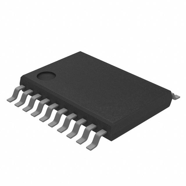
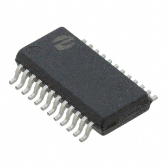
| 描述 | IC 8-BIT FET BUS SW 20-TSSOP数字总线开关 IC 8-Bit FET |
| 产品分类 | |
| 品牌 | Texas Instruments |
| 产品手册 | |
| 产品图片 |
|
| rohs | 符合RoHS无铅 / 符合限制有害物质指令(RoHS)规范要求 |
| 产品系列 | 开关 IC,数字总线开关 IC,Texas Instruments SN74CBT3345PWR74CBT |
| 数据手册 | |
| 产品型号 | SN74CBT3345PWR |
| 产品目录页面 | |
| 产品种类 | 数字总线开关 IC |
| 传播延迟时间 | 0.25 ns |
| 供应商器件封装 | 20-TSSOP |
| 其它名称 | 296-6442-1 |
| 包装 | 剪切带 (CT) |
| 单位重量 | 77 mg |
| 商标 | Texas Instruments |
| 安装类型 | 表面贴装 |
| 安装风格 | SMD/SMT |
| 导通电阻—最大值 | 7 Ohms |
| 封装 | Reel |
| 封装/外壳 | 20-TSSOP(0.173",4.40mm 宽) |
| 封装/箱体 | TSSOP-20 |
| 工作温度 | -40°C ~ 85°C |
| 工厂包装数量 | 2000 |
| 开关数量 | 8 |
| 技术 | CBT |
| 最大工作温度 | + 85 C |
| 最小工作温度 | - 40 C |
| 标准包装 | 1 |
| 独立电路 | 1 |
| 电压-电源 | 4.5 V ~ 5.5 V |
| 电压源 | 单电源 |
| 电流-输出高,低 | - |
| 电源电压-最大 | 5.5 V |
| 电源电压-最小 | 4 V |
| 电源电流 | 50 uA |
| 电路 | 8 x 1:1 |
| 类型 | FET 总线开关 |
| 系列 | SN74CBT3345 |
| 逻辑系列 | CBT |


- 商务部:美国ITC正式对集成电路等产品启动337调查
- 曝三星4nm工艺存在良率问题 高通将骁龙8 Gen1或转产台积电
- 太阳诱电将投资9.5亿元在常州建新厂生产MLCC 预计2023年完工
- 英特尔发布欧洲新工厂建设计划 深化IDM 2.0 战略
- 台积电先进制程称霸业界 有大客户加持明年业绩稳了
- 达到5530亿美元!SIA预计今年全球半导体销售额将创下新高
- 英特尔拟将自动驾驶子公司Mobileye上市 估值或超500亿美元
- 三星加码芯片和SET,合并消费电子和移动部门,撤换高东真等 CEO
- 三星电子宣布重大人事变动 还合并消费电子和移动部门
- 海关总署:前11个月进口集成电路产品价值2.52万亿元 增长14.8%


PDF Datasheet 数据手册内容提取
(cid:1)(cid:2)(cid:3)(cid:4)(cid:5)(cid:6)(cid:7)(cid:8)(cid:8)(cid:4)(cid:9) (cid:10)(cid:11)(cid:6)(cid:12)(cid:7) (cid:13)(cid:14)(cid:7) (cid:6)(cid:15)(cid:1) (cid:1)(cid:16)(cid:12)(cid:7)(cid:5)(cid:17) SCDS027I − MAY 1995 − REVISED JANUARY 2004 (cid:1) Standard ’245-Type Pinout DB, DBQ, DGV, DW, OR PW PACKAGE (cid:1) 5-Ω Switch Connection Between Two Ports (TOP VIEW) (cid:1) TTL-Compatible Input Levels OE 1 20 VCC A1 2 19 OE description/ordering information A2 3 18 B1 The SN74CBT3345 provides eight bits of A3 4 17 B2 high-speed TTL-compatible bus switching in a A4 5 16 B3 standard ’245 device pinout. The low on-state A5 6 15 B4 resistance of the switch allows connections to be A6 7 14 B5 made with minimal propagation delay. A7 8 13 B6 A8 9 12 B7 The device is organized as one 8-bit switch bank GND 10 11 B8 with dual output-enable (OE and OE) inputs. When OE is low or OE is high, the switch is on, and port A is connected to port B. When OE is high and OE is low, the switch is open, and the high-impedance state exists between the two ports. ORDERING INFORMATION ORDERABLE TOP-SIDE TA PACKAGE† PART NUMBER MARKING Tube SN74CBT3345DW SSOOIICC −− DDWW CCBBTT33334455 Tape and reel SN74CBT3345DWR SSOP − DB Tape and reel SN74CBT3345DBR CU345 −−4400°CC ttoo 8855°CC SSOP (QSOP) − DBQ Tape and reel SN74CBT3345DBQR CBT3345 Tube SN74CBT3345PW TTSSSSOOPP −− PPWW CCUU334455 Tape and reel SN74CBT3345PWR TVSOP − DGV Tape and reel SN74CBT3345DGVR CU345 †Package drawings, standard packing quantities, thermal data, symbolization, and PCB design guidelines are available at www.ti.com/sc/package. FUNCTION TABLE INPUTS FFUUNNCCTTIIOONN OE OE H X A port = B port X L A port = B port L H Disconnect Please be aware that an important notice concerning availability, standard warranty, and use in critical applications of TexasInstruments semiconductor products and disclaimers thereto appears at the end of this data sheet. (cid:18)(cid:19)(cid:20)(cid:21)(cid:15)(cid:5)(cid:7)(cid:12)(cid:20)(cid:2) (cid:21)(cid:22)(cid:7)(cid:22) (cid:23)(cid:24)(cid:25)(cid:26)(cid:27)(cid:28)(cid:29)(cid:30)(cid:23)(cid:26)(cid:24) (cid:23)(cid:31) !"(cid:27)(cid:27)#(cid:24)(cid:30) (cid:29)(cid:31) (cid:26)(cid:25) $"%&(cid:23)!(cid:29)(cid:30)(cid:23)(cid:26)(cid:24) ’(cid:29)(cid:30)#( Copyright 2004, Texas Instruments Incorporated (cid:18)(cid:27)(cid:26)’"!(cid:30)(cid:31) !(cid:26)(cid:24)(cid:25)(cid:26)(cid:27)(cid:28) (cid:30)(cid:26) (cid:31)$#!(cid:23)(cid:25)(cid:23)!(cid:29)(cid:30)(cid:23)(cid:26)(cid:24)(cid:31) $#(cid:27) (cid:30))# (cid:30)#(cid:27)(cid:28)(cid:31) (cid:26)(cid:25) (cid:7)#*(cid:29)(cid:31) (cid:12)(cid:24)(cid:31)(cid:30)(cid:27)"(cid:28)#(cid:24)(cid:30)(cid:31) (cid:31)(cid:30)(cid:29)(cid:24)’(cid:29)(cid:27)’ +(cid:29)(cid:27)(cid:27)(cid:29)(cid:24)(cid:30),( (cid:18)(cid:27)(cid:26)’"!(cid:30)(cid:23)(cid:26)(cid:24) $(cid:27)(cid:26)!#(cid:31)(cid:31)(cid:23)(cid:24)- ’(cid:26)#(cid:31) (cid:24)(cid:26)(cid:30) (cid:24)#!#(cid:31)(cid:31)(cid:29)(cid:27)(cid:23)&, (cid:23)(cid:24)!&"’# (cid:30)#(cid:31)(cid:30)(cid:23)(cid:24)- (cid:26)(cid:25) (cid:29)&& $(cid:29)(cid:27)(cid:29)(cid:28)#(cid:30)#(cid:27)(cid:31)( POST OFFICE BOX 655303 • DALLAS, TEXAS 75265 1
(cid:1)(cid:2)(cid:3)(cid:4)(cid:5)(cid:6)(cid:7)(cid:8)(cid:8)(cid:4)(cid:9) (cid:10)(cid:11)(cid:6)(cid:12)(cid:7) (cid:13)(cid:14)(cid:7) (cid:6)(cid:15)(cid:1) (cid:1)(cid:16)(cid:12)(cid:7)(cid:5)(cid:17) SCDS027I − MAY 1995 − REVISED JANUARY 2004 logic diagram (positive logic) 2 18 A1 B1 9 11 A8 B8 1 OE 19 OE absolute maximum ratings over operating free-air temperature range (unless otherwise noted)† Supply voltage range, V . . . . . . . . . . . . . . . . . . . . . . . . . . . . . . . . . . . . . . . . . . . . . . . . . . . . . . . . . . −0.5 V to 7 V CC Input voltage range, V (see Note 1) . . . . . . . . . . . . . . . . . . . . . . . . . . . . . . . . . . . . . . . . . . . . . . . . . . −0.5 V to 7 V I Continuous channel current . . . . . . . . . . . . . . . . . . . . . . . . . . . . . . . . . . . . . . . . . . . . . . . . . . . . . . . . . . . . . . 128 mA Input clamp current, IIK (VI/O < 0) . . . . . . . . . . . . . . . . . . . . . . . . . . . . . . . . . . . . . . . . . . . . . . . . . . . . . . . . . −50 mA Package thermal impedance, θ (see Note 2): DB package . . . . . . . . . . . . . . . . . . . . . . . . . . . . . . . . . . . . 70°C JA DBQ package . . . . . . . . . . . . . . . . . . . . . . . . . . . . . . . . . . . 68°C DGV package . . . . . . . . . . . . . . . . . . . . . . . . . . . . . . . . . . . 92°C DW package . . . . . . . . . . . . . . . . . . . . . . . . . . . . . . . . . . . . 58°C PW package . . . . . . . . . . . . . . . . . . . . . . . . . . . . . . . . . . . . 83°C Storage temperature range, T . . . . . . . . . . . . . . . . . . . . . . . . . . . . . . . . . . . . . . . . . . . . . . . . . . . −65°C to 150°C stg †Stresses beyond those listed under “absolute maximum ratings” may cause permanent damage to the device. These are stress ratings only, and functional operation of the device at these or any other conditions beyond those indicated under “recommended operating conditions” is not implied. Exposure to absolute-maximum-rated conditions for extended periods may affect device reliability. NOTES: 1. The input and output negative-voltage ratings may be exceeded if the input and output clamp-current ratings are observed. 2. The package thermal impedance is calculated in accordance with JESD 51-7. recommended operating conditions (see Note 3) MIN MAX UNIT VCC Supply voltage 4.5 5.5 V VIH High-level control input voltage 2 V VIL Low-level control input voltage 0.8 V TA Operating free-air temperature −40 85 °C NOTE 3: All unused control inputs of the device must be held at VCC or GND to ensure proper device operation. Refer to the TI application report, Implications of Slow or Floating CMOS Inputs, literature number SCBA004. 2 POST OFFICE BOX 655303 • DALLAS, TEXAS 75265
(cid:1)(cid:2)(cid:3)(cid:4)(cid:5)(cid:6)(cid:7)(cid:8)(cid:8)(cid:4)(cid:9) (cid:10)(cid:11)(cid:6)(cid:12)(cid:7) (cid:13)(cid:14)(cid:7) (cid:6)(cid:15)(cid:1) (cid:1)(cid:16)(cid:12)(cid:7)(cid:5)(cid:17) SCDS027I − MAY 1995 − REVISED JANUARY 2004 electrical characteristics over recommended operating free-air temperature range (unless otherwise noted) PARAMETER TEST CONDITIONS MIN TYP† MAX UNIT VIK VCC = 4.5 V, II = −18 mA −1.2 V II All inputs VCC = 5.5 V, VI = 5.5 V or GND ±1 µA ICC VCC = 5.5 V, IO = 0, VI = VCC or GND 50 µA ∆ICC‡ Control inputs VCC = 5.5 V, One input at 3.4 V, Other inputs at VCC or GND 3.5 mA Ci Control inputs VI = 3 V or 0 3 pF Cio(OFF) VO = 3 V or 0, OE = VCC or OE = GND 6 pF II = 64 mA 5 7 rroonn§ VVCCCC == 44..55 VV VVII == 00 II = 30 mA 5 7 Ω VI = 2.4 V, II = 15 mA 10 15 †All typical values are at VCC = 5 V, TA = 25°C. ‡This is the increase in supply current for each input that is at the specified TTL voltage level, rather than VCC or GND. §Measured by the voltage drop between the A and B terminals at the indicated current through the switch. On-state resistance is determined by the lower of the voltages of the two (A or B) terminals. switching characteristics over recommended operating free-air temperature range, C = 50 pF L (unless otherwise noted) (see Figure 1) VCC = 5 V PPAARRAAMMEETTEERR FROM TO ±0.5 V UUNNIITT ((IINNPPUUTT)) ((OOUUTTPPUUTT)) MIN MAX tpd¶ A or B B or A 0.25 ns ten OE or OE A or B 1 9.1 ns tdis OE or OE A or B 1 8.7 ns ¶The propagation delay is the calculated RC time constant of the typical on-state resistance of the switch and the specified load capacitance, when driven by an ideal voltage source (zero output impedance). POST OFFICE BOX 655303 • DALLAS, TEXAS 75265 3
(cid:1)(cid:2)(cid:3)(cid:4)(cid:5)(cid:6)(cid:7)(cid:8)(cid:8)(cid:4)(cid:9) (cid:10)(cid:11)(cid:6)(cid:12)(cid:7) (cid:13)(cid:14)(cid:7) (cid:6)(cid:15)(cid:1) (cid:1)(cid:16)(cid:12)(cid:7)(cid:5)(cid:17) SCDS027I − MAY 1995 − REVISED JANUARY 2004 PARAMETER MEASUREMENT INFORMATION 7 V TEST S1 From Output 500 Ω S1 Open tpd Open Under Test GND tPLZ/tPZL 7 V CL = 50 pF 500 Ω tPHZ/tPZH Open (see Note A) 3 V Output 1.5 V 1.5 V LOAD CIRCUIT Control 0 V tPZL tPLZ Output 3.5 V 3 V Waveform 1 1.5 V Input 1.5 V 1.5 V S1 at 7 V VOL + 0.3 V 0 V (see Note B) VOL tPZH tPHZ tPLH tPHL Output VOH VOH Waveform 2 1.5 V VOH − 0.3 V Output 1.5 V 1.5 V S1 at Open VOL (see Note B) 0 V VOLTAGE WAVEFORMS VOLTAGE WAVEFORMS PROPAGATION DELAY TIMES ENABLE AND DISABLE TIMES NOTES: A. CL includes probe and jig capacitance. B. Waveform 1 is for an output with internal conditions such that the output is low except when disabled by the output control. Waveform 2 is for an output with internal conditions such that the output is high except when disabled by the output control. C. All input pulses are supplied by generators having the following characteristics: PRR ≤10 MHz, ZO = 50 Ω, tr ≤2.5 ns, tf ≤2.5 ns. D. The outputs are measured one at a time with one transition per measurement. E. tPLZ and tPHZ are the same as tdis. F. tPZL and tPZH are the same as ten. G. tPLH and tPHL are the same as tpd. Figure 1. Load Circuit and Voltage Waveforms 4 POST OFFICE BOX 655303 • DALLAS, TEXAS 75265
PACKAGE OPTION ADDENDUM www.ti.com 17-Mar-2017 PACKAGING INFORMATION Orderable Device Status Package Type Package Pins Package Eco Plan Lead/Ball Finish MSL Peak Temp Op Temp (°C) Device Marking Samples (1) Drawing Qty (2) (6) (3) (4/5) SN74CBT3345DGVR ACTIVE TVSOP DGV 20 2000 Green (RoHS CU NIPDAU Level-1-260C-UNLIM -40 to 85 CU345 & no Sb/Br) SN74CBT3345DW ACTIVE SOIC DW 20 25 Green (RoHS CU NIPDAU Level-1-260C-UNLIM -40 to 85 CBT3345 & no Sb/Br) SN74CBT3345DWR ACTIVE SOIC DW 20 2000 Green (RoHS CU NIPDAU Level-1-260C-UNLIM -40 to 85 CBT3345 & no Sb/Br) SN74CBT3345PW ACTIVE TSSOP PW 20 70 Green (RoHS CU NIPDAU Level-1-260C-UNLIM -40 to 85 CU345 & no Sb/Br) SN74CBT3345PWR ACTIVE TSSOP PW 20 2000 Green (RoHS CU NIPDAU Level-1-260C-UNLIM -40 to 85 CU345 & no Sb/Br) (1) The marketing status values are defined as follows: ACTIVE: Product device recommended for new designs. LIFEBUY: TI has announced that the device will be discontinued, and a lifetime-buy period is in effect. NRND: Not recommended for new designs. Device is in production to support existing customers, but TI does not recommend using this part in a new design. PREVIEW: Device has been announced but is not in production. Samples may or may not be available. OBSOLETE: TI has discontinued the production of the device. (2) Eco Plan - The planned eco-friendly classification: Pb-Free (RoHS), Pb-Free (RoHS Exempt), or Green (RoHS & no Sb/Br) - please check http://www.ti.com/productcontent for the latest availability information and additional product content details. TBD: The Pb-Free/Green conversion plan has not been defined. Pb-Free (RoHS): TI's terms "Lead-Free" or "Pb-Free" mean semiconductor products that are compatible with the current RoHS requirements for all 6 substances, including the requirement that lead not exceed 0.1% by weight in homogeneous materials. Where designed to be soldered at high temperatures, TI Pb-Free products are suitable for use in specified lead-free processes. Pb-Free (RoHS Exempt): This component has a RoHS exemption for either 1) lead-based flip-chip solder bumps used between the die and package, or 2) lead-based die adhesive used between the die and leadframe. The component is otherwise considered Pb-Free (RoHS compatible) as defined above. Green (RoHS & no Sb/Br): TI defines "Green" to mean Pb-Free (RoHS compatible), and free of Bromine (Br) and Antimony (Sb) based flame retardants (Br or Sb do not exceed 0.1% by weight in homogeneous material) (3) MSL, Peak Temp. - The Moisture Sensitivity Level rating according to the JEDEC industry standard classifications, and peak solder temperature. (4) There may be additional marking, which relates to the logo, the lot trace code information, or the environmental category on the device. (5) Multiple Device Markings will be inside parentheses. Only one Device Marking contained in parentheses and separated by a "~" will appear on a device. If a line is indented then it is a continuation of the previous line and the two combined represent the entire Device Marking for that device. Addendum-Page 1
PACKAGE OPTION ADDENDUM www.ti.com 17-Mar-2017 (6) Lead/Ball Finish - Orderable Devices may have multiple material finish options. Finish options are separated by a vertical ruled line. Lead/Ball Finish values may wrap to two lines if the finish value exceeds the maximum column width. Important Information and Disclaimer:The information provided on this page represents TI's knowledge and belief as of the date that it is provided. TI bases its knowledge and belief on information provided by third parties, and makes no representation or warranty as to the accuracy of such information. Efforts are underway to better integrate information from third parties. TI has taken and continues to take reasonable steps to provide representative and accurate information but may not have conducted destructive testing or chemical analysis on incoming materials and chemicals. TI and TI suppliers consider certain information to be proprietary, and thus CAS numbers and other limited information may not be available for release. In no event shall TI's liability arising out of such information exceed the total purchase price of the TI part(s) at issue in this document sold by TI to Customer on an annual basis. Addendum-Page 2
PACKAGE MATERIALS INFORMATION www.ti.com 22-Jan-2015 TAPE AND REEL INFORMATION *Alldimensionsarenominal Device Package Package Pins SPQ Reel Reel A0 B0 K0 P1 W Pin1 Type Drawing Diameter Width (mm) (mm) (mm) (mm) (mm) Quadrant (mm) W1(mm) SN74CBT3345DGVR TVSOP DGV 20 2000 330.0 12.4 6.9 5.6 1.6 8.0 12.0 Q1 SN74CBT3345DWR SOIC DW 20 2000 330.0 24.4 10.8 13.3 2.7 12.0 24.0 Q1 SN74CBT3345PWR TSSOP PW 20 2000 330.0 16.4 6.95 7.1 1.6 8.0 16.0 Q1 PackMaterials-Page1
PACKAGE MATERIALS INFORMATION www.ti.com 22-Jan-2015 *Alldimensionsarenominal Device PackageType PackageDrawing Pins SPQ Length(mm) Width(mm) Height(mm) SN74CBT3345DGVR TVSOP DGV 20 2000 367.0 367.0 35.0 SN74CBT3345DWR SOIC DW 20 2000 367.0 367.0 45.0 SN74CBT3345PWR TSSOP PW 20 2000 367.0 367.0 38.0 PackMaterials-Page2
MECHANICAL DATA MPDS006C – FEBRUARY 1996 – REVISED AUGUST 2000 DGV (R-PDSO-G**) PLASTIC SMALL-OUTLINE 24 PINS SHOWN 0,23 0,40 0,07 M 0,13 24 13 0,16 NOM 4,50 6,60 4,30 6,20 Gage Plane 0,25 0°–(cid:1)8° 0,75 1 12 0,50 A Seating Plane 0,15 1,20 MAX 0,08 0,05 PINS ** 14 16 20 24 38 48 56 DIM A MAX 3,70 3,70 5,10 5,10 7,90 9,80 11,40 A MIN 3,50 3,50 4,90 4,90 7,70 9,60 11,20 4073251/E 08/00 NOTES: A. All linear dimensions are in millimeters. B. This drawing is subject to change without notice. C. Body dimensions do not include mold flash or protrusion, not to exceed 0,15 per side. D. Falls within JEDEC: 24/48 Pins – MO-153 14/16/20/56 Pins – MO-194 • POST OFFICE BOX 655303 DALLAS, TEXAS 75265
None
None
PACKAGE OUTLINE DW0020A SOIC - 2.65 mm max height SCALE 1.200 SOIC C 10.63 SEATING PLANE TYP 9.97 A PIN 1 ID 0.1 C AREA 18X 1.27 20 1 13.0 2X 12.6 11.43 NOTE 3 10 11 0.51 20X 7.6 0.31 2.65 MAX B 7.4 0.25 C A B NOTE 4 0.33 TYP 0.10 0.25 SEE DETAIL A GAGE PLANE 0.3 1.27 0 - 8 0.1 0.40 DETAIL A TYPICAL 4220724/A 05/2016 NOTES: 1. All linear dimensions are in millimeters. Dimensions in parenthesis are for reference only. Dimensioning and tolerancing per ASME Y14.5M. 2. This drawing is subject to change without notice. 3. This dimension does not include mold flash, protrusions, or gate burrs. Mold flash, protrusions, or gate burrs shall not exceed 0.15 mm per side. 4. This dimension does not include interlead flash. Interlead flash shall not exceed 0.43 mm per side. 5. Reference JEDEC registration MS-013. www.ti.com
EXAMPLE BOARD LAYOUT DW0020A SOIC - 2.65 mm max height SOIC 20X (2) SYMM 1 20 20X (0.6) 18X (1.27) SYMM (R0.05) TYP 10 11 (9.3) LAND PATTERN EXAMPLE SCALE:6X SOOPLEDNEINRG MASK METAL MSOELTDAEL RU NMDAESRK SOOPLEDNEINRG MASK 0.07 MAX 0.07 MIN ALL AROUND ALL AROUND NON SOLDER MASK SOLDER MASK DEFINED DEFINED SOLDER MASK DETAILS 4220724/A 05/2016 NOTES: (continued) 6. Publication IPC-7351 may have alternate designs. 7. Solder mask tolerances between and around signal pads can vary based on board fabrication site. www.ti.com
EXAMPLE STENCIL DESIGN DW0020A SOIC - 2.65 mm max height SOIC 20X (2) SYMM 1 20 20X (0.6) 18X (1.27) SYMM 10 11 (9.3) SOLDER PASTE EXAMPLE BASED ON 0.125 mm THICK STENCIL SCALE:6X 4220724/A 05/2016 NOTES: (continued) 8. Laser cutting apertures with trapezoidal walls and rounded corners may offer better paste release. IPC-7525 may have alternate design recommendations. 9. Board assembly site may have different recommendations for stencil design. www.ti.com
IMPORTANTNOTICE TexasInstrumentsIncorporated(TI)reservestherighttomakecorrections,enhancements,improvementsandotherchangestoits semiconductorproductsandservicesperJESD46,latestissue,andtodiscontinueanyproductorserviceperJESD48,latestissue.Buyers shouldobtainthelatestrelevantinformationbeforeplacingordersandshouldverifythatsuchinformationiscurrentandcomplete. TI’spublishedtermsofsaleforsemiconductorproducts(http://www.ti.com/sc/docs/stdterms.htm)applytothesaleofpackagedintegrated circuitproductsthatTIhasqualifiedandreleasedtomarket.AdditionaltermsmayapplytotheuseorsaleofothertypesofTIproductsand services. ReproductionofsignificantportionsofTIinformationinTIdatasheetsispermissibleonlyifreproductioniswithoutalterationandis accompaniedbyallassociatedwarranties,conditions,limitations,andnotices.TIisnotresponsibleorliableforsuchreproduced documentation.Informationofthirdpartiesmaybesubjecttoadditionalrestrictions.ResaleofTIproductsorserviceswithstatements differentfromorbeyondtheparametersstatedbyTIforthatproductorservicevoidsallexpressandanyimpliedwarrantiesforthe associatedTIproductorserviceandisanunfairanddeceptivebusinesspractice.TIisnotresponsibleorliableforanysuchstatements. BuyersandotherswhoaredevelopingsystemsthatincorporateTIproducts(collectively,“Designers”)understandandagreethatDesigners remainresponsibleforusingtheirindependentanalysis,evaluationandjudgmentindesigningtheirapplicationsandthatDesignershave fullandexclusiveresponsibilitytoassurethesafetyofDesigners'applicationsandcomplianceoftheirapplications(andofallTIproducts usedinorforDesigners’applications)withallapplicableregulations,lawsandotherapplicablerequirements.Designerrepresentsthat,with respecttotheirapplications,Designerhasallthenecessaryexpertisetocreateandimplementsafeguardsthat(1)anticipatedangerous consequencesoffailures,(2)monitorfailuresandtheirconsequences,and(3)lessenthelikelihoodoffailuresthatmightcauseharmand takeappropriateactions.DesigneragreesthatpriortousingordistributinganyapplicationsthatincludeTIproducts,Designerwill thoroughlytestsuchapplicationsandthefunctionalityofsuchTIproductsasusedinsuchapplications. TI’sprovisionoftechnical,applicationorotherdesignadvice,qualitycharacterization,reliabilitydataorotherservicesorinformation, including,butnotlimitedto,referencedesignsandmaterialsrelatingtoevaluationmodules,(collectively,“TIResources”)areintendedto assistdesignerswhoaredevelopingapplicationsthatincorporateTIproducts;bydownloading,accessingorusingTIResourcesinany way,Designer(individuallyor,ifDesignerisactingonbehalfofacompany,Designer’scompany)agreestouseanyparticularTIResource solelyforthispurposeandsubjecttothetermsofthisNotice. TI’sprovisionofTIResourcesdoesnotexpandorotherwisealterTI’sapplicablepublishedwarrantiesorwarrantydisclaimersforTI products,andnoadditionalobligationsorliabilitiesarisefromTIprovidingsuchTIResources.TIreservestherighttomakecorrections, enhancements,improvementsandotherchangestoitsTIResources.TIhasnotconductedanytestingotherthanthatspecifically describedinthepublisheddocumentationforaparticularTIResource. Designerisauthorizedtouse,copyandmodifyanyindividualTIResourceonlyinconnectionwiththedevelopmentofapplicationsthat includetheTIproduct(s)identifiedinsuchTIResource.NOOTHERLICENSE,EXPRESSORIMPLIED,BYESTOPPELOROTHERWISE TOANYOTHERTIINTELLECTUALPROPERTYRIGHT,ANDNOLICENSETOANYTECHNOLOGYORINTELLECTUALPROPERTY RIGHTOFTIORANYTHIRDPARTYISGRANTEDHEREIN,includingbutnotlimitedtoanypatentright,copyright,maskworkright,or otherintellectualpropertyrightrelatingtoanycombination,machine,orprocessinwhichTIproductsorservicesareused.Information regardingorreferencingthird-partyproductsorservicesdoesnotconstitutealicensetousesuchproductsorservices,orawarrantyor endorsementthereof.UseofTIResourcesmayrequirealicensefromathirdpartyunderthepatentsorotherintellectualpropertyofthe thirdparty,oralicensefromTIunderthepatentsorotherintellectualpropertyofTI. TIRESOURCESAREPROVIDED“ASIS”ANDWITHALLFAULTS.TIDISCLAIMSALLOTHERWARRANTIESOR REPRESENTATIONS,EXPRESSORIMPLIED,REGARDINGRESOURCESORUSETHEREOF,INCLUDINGBUTNOTLIMITEDTO ACCURACYORCOMPLETENESS,TITLE,ANYEPIDEMICFAILUREWARRANTYANDANYIMPLIEDWARRANTIESOF MERCHANTABILITY,FITNESSFORAPARTICULARPURPOSE,ANDNON-INFRINGEMENTOFANYTHIRDPARTYINTELLECTUAL PROPERTYRIGHTS.TISHALLNOTBELIABLEFORANDSHALLNOTDEFENDORINDEMNIFYDESIGNERAGAINSTANYCLAIM, INCLUDINGBUTNOTLIMITEDTOANYINFRINGEMENTCLAIMTHATRELATESTOORISBASEDONANYCOMBINATIONOF PRODUCTSEVENIFDESCRIBEDINTIRESOURCESOROTHERWISE.INNOEVENTSHALLTIBELIABLEFORANYACTUAL, DIRECT,SPECIAL,COLLATERAL,INDIRECT,PUNITIVE,INCIDENTAL,CONSEQUENTIALOREXEMPLARYDAMAGESIN CONNECTIONWITHORARISINGOUTOFTIRESOURCESORUSETHEREOF,ANDREGARDLESSOFWHETHERTIHASBEEN ADVISEDOFTHEPOSSIBILITYOFSUCHDAMAGES. UnlessTIhasexplicitlydesignatedanindividualproductasmeetingtherequirementsofaparticularindustrystandard(e.g.,ISO/TS16949 andISO26262),TIisnotresponsibleforanyfailuretomeetsuchindustrystandardrequirements. WhereTIspecificallypromotesproductsasfacilitatingfunctionalsafetyorascompliantwithindustryfunctionalsafetystandards,such productsareintendedtohelpenablecustomerstodesignandcreatetheirownapplicationsthatmeetapplicablefunctionalsafetystandards andrequirements.Usingproductsinanapplicationdoesnotbyitselfestablishanysafetyfeaturesintheapplication.Designersmust ensurecompliancewithsafety-relatedrequirementsandstandardsapplicabletotheirapplications.DesignermaynotuseanyTIproductsin life-criticalmedicalequipmentunlessauthorizedofficersofthepartieshaveexecutedaspecialcontractspecificallygoverningsuchuse. Life-criticalmedicalequipmentismedicalequipmentwherefailureofsuchequipmentwouldcauseseriousbodilyinjuryordeath(e.g.,life support,pacemakers,defibrillators,heartpumps,neurostimulators,andimplantables).Suchequipmentincludes,withoutlimitation,all medicaldevicesidentifiedbytheU.S.FoodandDrugAdministrationasClassIIIdevicesandequivalentclassificationsoutsidetheU.S. TImayexpresslydesignatecertainproductsascompletingaparticularqualification(e.g.,Q100,MilitaryGrade,orEnhancedProduct). Designersagreethatithasthenecessaryexpertisetoselecttheproductwiththeappropriatequalificationdesignationfortheirapplications andthatproperproductselectionisatDesigners’ownrisk.Designersaresolelyresponsibleforcompliancewithalllegalandregulatory requirementsinconnectionwithsuchselection. DesignerwillfullyindemnifyTIanditsrepresentativesagainstanydamages,costs,losses,and/orliabilitiesarisingoutofDesigner’snon- compliancewiththetermsandprovisionsofthisNotice. MailingAddress:TexasInstruments,PostOfficeBox655303,Dallas,Texas75265 Copyright©2017,TexasInstrumentsIncorporated