ICGOO在线商城 > 集成电路(IC) > 逻辑 - 信号开关,多路复用器,解码器 > SN74CB3Q3345PWR

 Datasheet下载
- 型号: SN74CB3Q3345PWR
- 制造商: Texas Instruments
- 库位|库存: xxxx|xxxx
- 要求:
| 数量阶梯 | 香港交货 | 国内含税 |
| +xxxx | $xxxx | ¥xxxx |
查看当月历史价格
查看今年历史价格
SN74CB3Q3345PWR产品简介:
ICGOO电子元器件商城为您提供SN74CB3Q3345PWR由Texas Instruments设计生产,在icgoo商城现货销售,并且可以通过原厂、代理商等渠道进行代购。 SN74CB3Q3345PWR价格参考¥2.42-¥5.98。Texas InstrumentsSN74CB3Q3345PWR封装/规格:逻辑 - 信号开关,多路复用器,解码器, Bus Switch 8 x 1:1 20-TSSOP。您可以下载SN74CB3Q3345PWR参考资料、Datasheet数据手册功能说明书,资料中有SN74CB3Q3345PWR 详细功能的应用电路图电压和使用方法及教程。
SN74CB3Q3345PWR 是由 Texas Instruments(德州仪器)生产的一款逻辑芯片,属于信号开关、多路复用器和解码器类别。该器件主要应用于需要高效信号切换、数据路由以及复杂逻辑控制的场景。以下是其典型应用场景:

1. 通信系统
   在通信设备中,SN74CB3Q3345PWR 可用于信号路径的选择与切换,例如在多通道收发器中实现数据流的动态分配。它能够支持高速信号传输,确保数据完整性并减少延迟。

2. 计算机外设与接口设计
   该芯片适用于 USB、PCIe 等高速接口的设计中,作为信号切换的核心组件。通过多路复用功能,可以灵活管理多个输入/输出端口之间的连接关系。

3. 嵌入式系统中的资源管理
   在微控制器或 FPGA 系统中,这款 IC 能够帮助优化硬件资源分配。例如,在有限的引脚数情况下,通过多路复用技术共享某些外围设备(如传感器或存储器模块)。

4. 音频视频处理设备
   对于 AV 切换器、投影仪或其他多媒体装置而言,此型号可用于选择不同来源的音视频信号,并将其传递给正确的输出端。

5. 工业自动化控制系统
   工业领域常涉及复杂的信号网络,SN74CB3Q3345PWR 可以协助完成对各种现场总线协议的支持及转换任务,同时提供可靠的电气隔离特性。

6. 测试测量仪器
   在示波器、逻辑分析仪等精密仪器内,此类器件有助于实现快速精确地捕获和处理来自不同通道的电信号。

总之,SN74CB3Q3345PWR 凭借其卓越的性能参数(如低功耗、高频率操作能力),成为众多现代电子产品的理想选择,尤其适合那些要求高性能、灵活性和稳定性的应用场合。
| 参数 | 数值 |
| 产品目录 | 集成电路 (IC)半导体 |
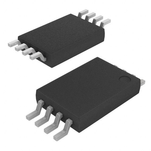
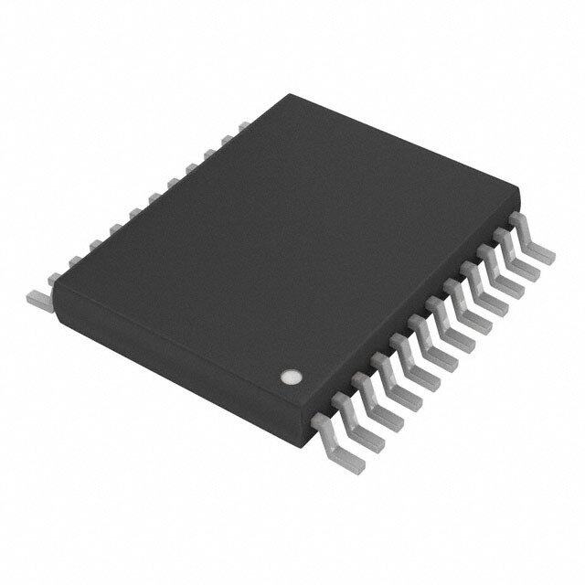
| 描述 | IC SWITCH BUS 8BIT FET 20-TSSOP数字总线开关 IC Lo-Vltg Hi-Bandwidth Bus Switch |
| 产品分类 | |
| 品牌 | Texas Instruments |
| 产品手册 | |
| 产品图片 |
|
| rohs | 符合RoHS无铅 / 符合限制有害物质指令(RoHS)规范要求 |
| 产品系列 | 开关 IC,数字总线开关 IC,Texas Instruments SN74CB3Q3345PWR74CB |
| 数据手册 | |
| 产品型号 | SN74CB3Q3345PWR |
| 产品目录页面 | |
| 产品种类 | 数字总线开关 IC |
| 传播延迟时间 | 0.2 ns |
| 供应商器件封装 | 20-TSSOP |
| 其它名称 | 296-19141-1 |
| 包装 | 剪切带 (CT) |
| 单位重量 | 77 mg |
| 商标 | Texas Instruments |
| 安装类型 | 表面贴装 |
| 安装风格 | SMD/SMT |
| 导通电阻—最大值 | 9 Ohms |
| 封装 | Reel |
| 封装/外壳 | 20-TSSOP(0.173",4.40mm 宽) |
| 封装/箱体 | TSSOP-20 |
| 工作温度 | -40°C ~ 85°C |
| 工厂包装数量 | 2000 |
| 开关数量 | 8 |
| 技术 | CB3Q |
| 最大工作温度 | + 85 C |
| 最小工作温度 | - 40 C |
| 标准包装 | 1 |
| 独立电路 | 1 |
| 电压-电源 | 2.3 V ~ 3.6 V |
| 电压源 | 单电源 |
| 电流-输出高,低 | - |
| 电源电压-最大 | 3.6 V |
| 电源电压-最小 | 2.3 V |
| 电源电流 | 700 uA |
| 电路 | 8 x 1:1 |
| 类型 | FET 总线开关 |
| 系列 | SN74CB3Q3345 |
| 逻辑系列 | CB3Q |


- 商务部:美国ITC正式对集成电路等产品启动337调查
- 曝三星4nm工艺存在良率问题 高通将骁龙8 Gen1或转产台积电
- 太阳诱电将投资9.5亿元在常州建新厂生产MLCC 预计2023年完工
- 英特尔发布欧洲新工厂建设计划 深化IDM 2.0 战略
- 台积电先进制程称霸业界 有大客户加持明年业绩稳了
- 达到5530亿美元!SIA预计今年全球半导体销售额将创下新高
- 英特尔拟将自动驾驶子公司Mobileye上市 估值或超500亿美元
- 三星加码芯片和SET,合并消费电子和移动部门,撤换高东真等 CEO
- 三星电子宣布重大人事变动 还合并消费电子和移动部门
- 海关总署:前11个月进口集成电路产品价值2.52万亿元 增长14.8%


PDF Datasheet 数据手册内容提取
SN74CB3Q3345 8-BIT FET BUS SWITCH 2.5-V/3.3-V LOW-VOLTAGE HIGH-BANDWIDTH BUS SWITCH www.ti.com SCDS144B–OCTOBER2003–REVISEDMARCH2005 FEATURES • DataandControlInputsProvideUndershoot • High-BandwidthDataPath(upto500MHz (1)) ClampDiodes • 5-V-TolerantI/OsWithDevicePoweredUpor • LowPowerConsumption(ICC=0.7mATyp) PoweredDown • V OperatingRangeFrom2.3Vto3.6V CC • LowandFlatON-StateResistance(r ) • DataI/OsSupport0-to5-VSignalingLevels on CharacteristicsOverOperatingRange (0.8V,1.2V,1.5V,1.8V,2.5V,3.3V,5V) (ron=4W Typ) • ControlInputsCanBeDrivenbyTTLor • Rail-to-RailSwitchingonDataI/OPorts 5-V/3.3-VCMOSOutputs – 0-to5-VSwitchingWith3.3-VV • I SupportsPartial-Power-DownMode CC off – 0-to3.3-VSwitchingWith2.5-VV Operation CC • BidirectionalDataFlowWithNear-Zero • Latch-UpPerformanceExceeds100mAPer PropagationDelay JESD78,ClassII • LowInput/OutputCapacitanceMinimizes • ESDPerformanceTestedPerJESD22 LoadingandSignalDistortion – 2000-VHuman-BodyModel (C =4pFTyp) (A114-B,ClassII) io(OFF) • FastSwitchingFrequency(f =20MHzMax) – 1000-VCharged-DeviceModel(C101) OE • SupportsBothDigitalandAnalog (1) Foradditionalinformationregardingtheperformance Applications:DifferentialSignalInterface, characteristicsoftheCB3Qfamily,refertotheTIapplication MemoryInterleaving,BusIsolation, report,CBT-C,CB3T,andCB3QSignal-SwitchFamilies, literaturenumberSCDA008. Low-DistortionSignalGating DBQ, DGV, OR PW PACKAGE RGY PACKAGE (TOP VIEW) (TOP VIEW) C OE 1 20 VCC OE VC A1 2 19 OE 1 20 A2 3 18 B1 A1 2 19 OE A3 4 17 B2 A2 3 18 B1 A4 5 16 B3 A3 4 17 B2 A5 6 15 B4 A4 5 16 B9 A6 7 14 B5 A5 6 15 B4 A7 8 13 B6 A6 7 14 B5 A8 9 12 B7 A7 8 13 B6 GND 10 11 B8 A8 9 12 B7 10 11 D 8 N B G Pleasebeawarethatanimportantnoticeconcerningavailability,standardwarranty,anduseincriticalapplicationsofTexas Instrumentssemiconductorproductsanddisclaimerstheretoappearsattheendofthisdatasheet. PRODUCTIONDATAinformationiscurrentasofpublicationdate. Copyright©2003–2005,TexasInstrumentsIncorporated Products conform to specifications per the terms of the Texas Instruments standard warranty. Production processing does not necessarilyincludetestingofallparameters.
SN74CB3Q3345 8-BIT FET BUS SWITCH 2.5-V/3.3-V LOW-VOLTAGE HIGH-BANDWIDTH BUS SWITCH www.ti.com SCDS144B–OCTOBER2003–REVISEDMARCH2005 DESCRIPTION/ORDERING INFORMATION The SN74CB3Q3345 is a high-bandwidth FET bus switch utilizing a charge pump to elevate the gate voltage of thepasstransistor,providingalowand flat ON-state resistance (r ). The low and flat ON-state resistance allows on for minimal propagation delay and supports rail-to-rail switching on the data input/output (I/O) ports. The device also features low data I/O capacitance to minimize capacitive loading and signal distortion on the data bus. Specifically designed to support high-bandwidth applications, the SN74CB3Q3345 provides an optimized interface solution ideally suited for broadband communications, networking, and data-intensive computing systems. The SN74CB3Q3384A is organized as an 8-bit bus switch with two output-enable (OE, OE) inputs. When OE is highorOEislow,thebusswitchisON, and the A port is connected to the B port, allowing bidirectional data flow between ports. When OE is low and OE is high, the bus switch is OFF, and a high-impedance state exists betweentheAandBports. This device is fully specified for partial-power-down applications using I . The I circuitry prevents damaging off off currentbackflowthroughthedevicewhenitispowereddown.Thedevicehasisolationduringpoweroff. To ensure the high-impedance state during power up or power down, OE should be tied to V through a pullup CC resistor and OE should be tied to GND through a pulldown resistor; the minimum value of the resistor is determinedbythecurrent-sinking/current-sourcingcapabilityofthedriver. ORDERINGINFORMATION T PACKAGE(1) ORDERABLEPARTNUMBER TOP-SIDEMARKING A QFN–RGY Tapeandreel SN74CB3Q3345RGYR BU345 SSOP(QSOP)–DBQ Tapeandreel SN74CB3Q3345DBQR CB3Q3345 –40°Cto85°C Tube SN74CB3Q3345PW TSSOP–PW BU345 Tapeandreel SN74CB3Q3345PWR TVSOP–DGV Tapeandreel SN74CB3Q3345DGVR BU345 (1) Packagedrawings,standardpackingquantities,thermaldata,symbolization,andPCBdesignguidelinesareavailableat www.ti.com/sc/package. FUNCTIONTABLE INPUTS INPUT/OUTPUT FUNCTION OE OE A H X B Aport=Bport X L B Aport=Bport L H Z Disconnect LOGICDIAGRAM(POSITIVELOGIC) 2 18 A1 SW B1 9 11 A8 SW B8 1 OE 19 OE 2
SN74CB3Q3345 8-BIT FET BUS SWITCH 2.5-V/3.3-V LOW-VOLTAGE HIGH-BANDWIDTH BUS SWITCH www.ti.com SCDS144B–OCTOBER2003–REVISEDMARCH2005 SIMPLIFIED SCHEMATIC, EACH FET SWITCH (SW) A B VCC Charge Pump EN(1) (1) EN is the internal enable signal applied to the switch. Absolute Maximum Ratings(1) overoperatingfree-airtemperaturerange(unlessotherwisenoted) MIN MAX UNIT V Supplyvoltagerange –0.5 4.6 V CC V Controlinputvoltagerange(2)(3) –0.5 7 V IN V SwitchI/Ovoltagerange(2)(3)(4) –0.5 7 V I/O I Controlinputclampcurrent V <0 –50 mA I/K IN I I/Oportclampcurrent V <0 –50 mA I/OK I/O I ON-stateswitchcurrent(5) ±64 mA IO ContinuouscurrentthroughV orGND ±100 mA CC DBQpackage(6) 68 DGVpackage(6) 92 q Packagethermalimpedance °C/W JA PWpackage(6) 83 RGYpackage(7) 37 T Storagetemperaturerange –65 150 °C stg (1) Stressesbeyondthoselistedunder"absolutemaximumratings"maycausepermanentdamagetothedevice.Thesearestressratings only,andfunctionaloperationofthedeviceattheseoranyotherconditionsbeyondthoseindicatedunder"recommendedoperating conditions"isnotimplied.Exposuretoabsolute-maximum-ratedconditionsforextendedperiodsmayaffectdevicereliability. (2) Allvoltagesarewithrespecttoground,unlessotherwisespecified. (3) Theinputandoutputvoltageratingsmaybeexceedediftheinputandoutputclamp-currentratingsareobserved. (4) V andV areusedtodenotespecificconditionsforV . I O I/O (5) I andI areusedtodenotespecificconditionsforI . I O I/O (6) ThepackagethermalimpedanceiscalculatedinaccordancewithJESD51-7. (7) ThepackagethermalimpedanceiscalculatedinaccordancewithJESD51-5. 3
SN74CB3Q3345 8-BIT FET BUS SWITCH 2.5-V/3.3-V LOW-VOLTAGE HIGH-BANDWIDTH BUS SWITCH www.ti.com SCDS144B–OCTOBER2003–REVISEDMARCH2005 Recommended Operating Conditions(1) MIN MAX UNIT V Supplyvoltage 2.3 3.6 V CC V =2.3Vto2.7V 1.7 5.5 CC V High-levelcontrolinputvoltage V IH V =2.7Vto3.6V 2 5.5 CC V =2.3Vto2.7V 0 0.7 CC V Low-levelcontrolinputvoltage V IL V =2.7Vto3.6V 0 0.8 CC V Datainput/outputvoltage 0 5.5 V I/O T Operatingfree-airtemperature –40 85 °C A (1) AllunusedcontrolinputsofthedevicemustbeheldatV orGNDtoensureproperdeviceoperation.RefertotheTIapplicationreport, CC ImplicationsofSloworFloatingCMOSInputs,literaturenumberSCBA004. Electrical Characteristics(1) overrecommendedoperatingfree-airtemperaturerange(unlessotherwisenoted) PARAMETER TESTCONDITIONS MIN TYP(2) MAX UNIT V V =3.6V, I =–18mA –1.8 V IK CC I I Controlinputs V =3.6V, V =0to5.5V ±1 m A IN CC IN I (3) V =3.6V, VO=0to5.5V, SwitchOFF, ±1 m A OZ CC V =0, V =V orGND I IN CC I V =0, V =0to5.5V, V =0 1 m A off CC O I I =0, I V =3.6V, I/O V =V orGND 0.7 2 mA CC CC SwitchONorOFF, IN CC D I (4) Controlinputs V =3.6V, Oneinputat3V, OtherinputsatV orGND 30 m A CC CC CC I (5) Percontrol VCC=3.6V, AandBportsopen, 0.13 0.14 mA/ CCD input Controlinputswitchingat50%dutycycle MHz C Controlinputs V =3.3V, V =5.5V,3.3V,or0 2.5 3.5 pF in CC IN SwitchOFF, C V =3.3V, V =5.5V,3.3V,or0 3.5 5 pF io(OFF) CC V =V orGND, I/O IN CC SwitchON, C V =3.3V, V =5.5V,3.3V,or0 9 11.5 pF io(ON) CC V =V orGND, I/O IN CC VCC=2.3V, VI=0, IO=30mA 4 8 r (6) TYPatVCC=2.5V VI=1.7V, IO=–15mA 4.5 9 W on V =0, I =30mA 4 6 I O V =3V CC V =2.4V, I =–15mA 4.5 8 I O (1) V andI refertocontrolinputs.V,V ,I,andI refertodatapins. IN IN I O I O (2) AlltypicalvaluesareatV =3.3V(unlessotherwisenoted),T =25°C. CC A (3) ForI/Oports,theparameterI includestheinputleakagecurrent. OZ (4) ThisistheincreaseinsupplycurrentforeachinputthatisatthespecifiedTTLvoltagelevel,ratherthanV orGND. CC (5) Thisparameterspecifiesthedynamicpower-supplycurrentassociatedwiththeoperatingfrequencyofasinglecontrolinput(see Figure2). (6) MeasuredbythevoltagedropbetweentheAandBterminalsattheindicatedcurrentthroughtheswitch.ON-stateresistanceis determinedbythelowerofthevoltagesofthetwo(AorB)terminals. 4
SN74CB3Q3345 8-BIT FET BUS SWITCH 2.5-V/3.3-V LOW-VOLTAGE HIGH-BANDWIDTH BUS SWITCH www.ti.com SCDS144B–OCTOBER2003–REVISEDMARCH2005 Switching Characteristics overrecommendedoperatingfree-airtemperaturerange(unlessotherwisenoted)(seeFigure3) V =2.5V V =3.3V CC CC PARAMETER FROM TO ±0.2V ±0.3V UNIT (INPUT) (OUTPUT) MIN MAX MIN MAX f orf (1) OEorOE AorB 10 20 MHz OE OE t (2) AorB BorA 0.12 0.2 ns pd t OEorOE AorB 1.5 7.7 1.5 6.5 ns en t OEorOE AorB 1 6.9 1 6.8 ns dis (1) Maximumswitchingfrequencyforcontrolinput(V >V ,V =5V,R ‡ 1MW ,C =0) O CC I L L (2) ThepropagationdelayisthecalculatedRCtimeconstantofthetypicalON-stateresistanceoftheswitchandthespecifiedload capacitance,whendrivenbyanidealvoltagesource(zerooutputimpedance). TYPICAL r on vs V I 16 (cid:1)ce - 1124 VTIOAC =C= -=21 553° .mC3 VA n a st 10 si e R 8 e Stat 6 N- 4 O - n 2 o r 0 0.0 0.5 1.0 1.5 2.0 2.5 3.0 3.5 4.0 4.5 5.0 VI - V Figure1.Typicalr vsV on I TYPICAL I CC vs OE or OE SWITCHING FREQUENCY 12 VCC = 3.3 V 10 TA = 25 °C A and B Ports Open 8 A m − 6 C C I 4 2 One OE or OE Switching 0 0 2 4 6 8 10 12 14 16 18 20 OE or OE Switching Frequency − MHz Figure2.TypicalI vsOEorOESwitchingFrequency CC 5
SN74CB3Q3345 8-BIT FET BUS SWITCH 2.5-V/3.3-V LOW-VOLTAGE HIGH-BANDWIDTH BUS SWITCH www.ti.com SCDS144B–OCTOBER2003–REVISEDMARCH2005 PARAMETER MEASUREMENT INFORMATION VCC Input Generator VIN 50 W VG1 50 W TEST CIRCUIT DUT 2 × VCC Input Generator S1 VI VO RL Open 50 W GND VG2 50 W CL RL (see Note A) TEST VCC S1 RL VI CL VD tpd(s) 2.5 V ± 0.2 V Open 500 W VCC or GND 30 pF 3.3 V ± 0.3 V Open 500 W VCC or GND 50 pF tPLZ/tPZL 23..53 VV ±± 00..23 VV 22 ×× VVCCCC 550000 WW GGNNDD 3500 ppFF 00.1.35 V V tPHZ/tPZH 23..53 VV ±± 00..23 VV GGNNDD 550000 WW VVCCCC 3500 ppFF 00.1.35 V V Output VCC Control VCC/2 VCC/2 (VIN) 0 V tPZL tPLZ Output Output VCC Waveform 1 VCC Control VCC/2 VCC/2 S1 at 2 × VCC VCC/2 VOL + VD (VIN) 0 V (see Note B) VOL tPZH tPHZ tPLH tPHL Output VOH VOH Waveform 2 VOH − VD Output VCC/2 VCC/2 S1 at GND VCC/2 VOL (see Note B) 0 V VOLTAGE WAVEFORMS VOLTAGE WAVEFORMS PROPAGATION DELAY TIMES (tpd(s)) ENABLE AND DISABLE TIMES NOTES: A. CL includes probe and jig capacitance. B. Waveform 1 is for an output with internal conditions such that the output is low, except when disabled by the output control. Waveform 2 is for an output with internal conditions such that the output is high, except when disabled by the output control. C. All input pulses are supplied by generators having the following characteristics: PRR ≤ 10 MHz, ZO = 50 W , tr ≤ 2.5 ns, tf ≤ 2.5 ns. D. The outputs are measured one at a time, with one transition per measurement. E. tPLZ and tPHZ are the same as tdis. F. tPZL and tPZH are the same as ten. G. tPLH and tPHL are the same as tpd(s). The tpd propagation delay is the calculated RC time constant of the typical ON-state resistance of the switch and the specified load capacitance, when driven by an ideal voltage source (zero output impedance). H. All parameters and waveforms are not applicable to all devices. Figure3.TestCircuitandVoltageWaveforms 6
PACKAGE OPTION ADDENDUM www.ti.com 6-Feb-2020 PACKAGING INFORMATION Orderable Device Status Package Type Package Pins Package Eco Plan Lead/Ball Finish MSL Peak Temp Op Temp (°C) Device Marking Samples (1) Drawing Qty (2) (6) (3) (4/5) SN74CB3Q3345DBQR ACTIVE SSOP DBQ 20 2500 Green (RoHS NIPDAU Level-2-260C-1 YEAR -40 to 85 CB3Q3345 & no Sb/Br) SN74CB3Q3345DGVR ACTIVE TVSOP DGV 20 2000 Green (RoHS NIPDAU Level-1-260C-UNLIM -40 to 85 BU345 & no Sb/Br) SN74CB3Q3345PW ACTIVE TSSOP PW 20 70 Green (RoHS NIPDAU Level-1-260C-UNLIM -40 to 85 BU345 & no Sb/Br) SN74CB3Q3345PWR ACTIVE TSSOP PW 20 2000 Green (RoHS NIPDAU Level-1-260C-UNLIM -40 to 85 BU345 & no Sb/Br) SN74CB3Q3345RGYR ACTIVE VQFN RGY 20 3000 Green (RoHS NIPDAU Level-2-260C-1 YEAR -40 to 85 BU345 & no Sb/Br) (1) The marketing status values are defined as follows: ACTIVE: Product device recommended for new designs. LIFEBUY: TI has announced that the device will be discontinued, and a lifetime-buy period is in effect. NRND: Not recommended for new designs. Device is in production to support existing customers, but TI does not recommend using this part in a new design. PREVIEW: Device has been announced but is not in production. Samples may or may not be available. OBSOLETE: TI has discontinued the production of the device. (2) RoHS: TI defines "RoHS" to mean semiconductor products that are compliant with the current EU RoHS requirements for all 10 RoHS substances, including the requirement that RoHS substance do not exceed 0.1% by weight in homogeneous materials. Where designed to be soldered at high temperatures, "RoHS" products are suitable for use in specified lead-free processes. TI may reference these types of products as "Pb-Free". RoHS Exempt: TI defines "RoHS Exempt" to mean products that contain lead but are compliant with EU RoHS pursuant to a specific EU RoHS exemption. Green: TI defines "Green" to mean the content of Chlorine (Cl) and Bromine (Br) based flame retardants meet JS709B low halogen requirements of <=1000ppm threshold. Antimony trioxide based flame retardants must also meet the <=1000ppm threshold requirement. (3) MSL, Peak Temp. - The Moisture Sensitivity Level rating according to the JEDEC industry standard classifications, and peak solder temperature. (4) There may be additional marking, which relates to the logo, the lot trace code information, or the environmental category on the device. (5) Multiple Device Markings will be inside parentheses. Only one Device Marking contained in parentheses and separated by a "~" will appear on a device. If a line is indented then it is a continuation of the previous line and the two combined represent the entire Device Marking for that device. (6) Lead/Ball Finish - Orderable Devices may have multiple material finish options. Finish options are separated by a vertical ruled line. Lead/Ball Finish values may wrap to two lines if the finish value exceeds the maximum column width. Addendum-Page 1
PACKAGE OPTION ADDENDUM www.ti.com 6-Feb-2020 Important Information and Disclaimer:The information provided on this page represents TI's knowledge and belief as of the date that it is provided. TI bases its knowledge and belief on information provided by third parties, and makes no representation or warranty as to the accuracy of such information. Efforts are underway to better integrate information from third parties. TI has taken and continues to take reasonable steps to provide representative and accurate information but may not have conducted destructive testing or chemical analysis on incoming materials and chemicals. TI and TI suppliers consider certain information to be proprietary, and thus CAS numbers and other limited information may not be available for release. In no event shall TI's liability arising out of such information exceed the total purchase price of the TI part(s) at issue in this document sold by TI to Customer on an annual basis. Addendum-Page 2
PACKAGE MATERIALS INFORMATION www.ti.com 22-Jan-2015 TAPE AND REEL INFORMATION *Alldimensionsarenominal Device Package Package Pins SPQ Reel Reel A0 B0 K0 P1 W Pin1 Type Drawing Diameter Width (mm) (mm) (mm) (mm) (mm) Quadrant (mm) W1(mm) SN74CB3Q3345DBQR SSOP DBQ 20 2500 330.0 16.4 6.5 9.0 2.1 8.0 16.0 Q1 SN74CB3Q3345DGVR TVSOP DGV 20 2000 330.0 12.4 6.9 5.6 1.6 8.0 12.0 Q1 SN74CB3Q3345PWR TSSOP PW 20 2000 330.0 16.4 6.95 7.1 1.6 8.0 16.0 Q1 SN74CB3Q3345RGYR VQFN RGY 20 3000 330.0 12.4 3.8 4.8 1.6 8.0 12.0 Q1 PackMaterials-Page1
PACKAGE MATERIALS INFORMATION www.ti.com 22-Jan-2015 *Alldimensionsarenominal Device PackageType PackageDrawing Pins SPQ Length(mm) Width(mm) Height(mm) SN74CB3Q3345DBQR SSOP DBQ 20 2500 367.0 367.0 38.0 SN74CB3Q3345DGVR TVSOP DGV 20 2000 367.0 367.0 35.0 SN74CB3Q3345PWR TSSOP PW 20 2000 367.0 367.0 38.0 SN74CB3Q3345RGYR VQFN RGY 20 3000 367.0 367.0 35.0 PackMaterials-Page2
MECHANICAL DATA MPDS006C – FEBRUARY 1996 – REVISED AUGUST 2000 DGV (R-PDSO-G**) PLASTIC SMALL-OUTLINE 24 PINS SHOWN 0,23 0,40 0,07 M 0,13 24 13 0,16 NOM 4,50 6,60 4,30 6,20 Gage Plane 0,25 0°–(cid:1)8° 0,75 1 12 0,50 A Seating Plane 0,15 1,20 MAX 0,08 0,05 PINS ** 14 16 20 24 38 48 56 DIM A MAX 3,70 3,70 5,10 5,10 7,90 9,80 11,40 A MIN 3,50 3,50 4,90 4,90 7,70 9,60 11,20 4073251/E 08/00 NOTES: A. All linear dimensions are in millimeters. B. This drawing is subject to change without notice. C. Body dimensions do not include mold flash or protrusion, not to exceed 0,15 per side. D. Falls within JEDEC: 24/48 Pins – MO-153 14/16/20/56 Pins – MO-194 • POST OFFICE BOX 655303 DALLAS, TEXAS 75265
None
None
GENERIC PACKAGE VIEW RGY 20 VQFN - 1 mm max height 3.5 x 4.5, 0.5 mm pitch PLASTIC QUAD FGLATPACK - NO LEAD This image is a representation of the package family, actual package may vary. Refer to the product data sheet for package details. 4225264/A www.ti.com
PACKAGE OUTLINE RGY0020A VQFN - 1 mm max height SCALE 3.000 PLASTIC QUAD FLATPACK - NO LEAD A 3.65 B 3.35 PIN 1 INDEX AREA 4.65 4.35 1.0 0.8 C SEATING PLANE 0.05 0.00 0.08 C 2.05 0.1 2X 1.5 (0.2) TYP 10 11 EXPOSED THERMAL PAD 9 12 14X 0.5 2X SYMM 21 3.05 0.1 3.5 2 19 0.30 PIN 1 ID 1 20 20X 0.18 SYMM 0.1 C A B 0.5 0.05 20X 0.3 4225320/A 09/2019 NOTES: 1. All linear dimensions are in millimeters. Any dimensions in parenthesis are for reference only. Dimensioning and tolerancing per ASME Y14.5M. 2. This drawing is subject to change without notice. 3. The package thermal pad must be soldered to the printed circuit board for thermal and mechanical performance. www.ti.com
EXAMPLE BOARD LAYOUT RGY0020A VQFN - 1 mm max height PLASTIC QUAD FLATPACK - NO LEAD (2.05) SYMM 1 20 20X (0.6) 2 19 20X (0.24) (1.275) (4.3) SYMM 21 (3.05) 14X (0.5) (0.775) 9 12 (R0.05) TYP ( 0.2) TYP VIA 10 11 (0.75) TYP (3.3) LAND PATTERN EXAMPLE EXPOSED METAL SHOWN SCALE:18X 0.07 MAX 0.07 MIN ALL AROUND ALL AROUND SOLDER MASK METAL OPENING EXPOSED METAL SOLDER MASK EXPOSED METAL UNDER OPENING METAL SOLDER MASK NON SOLDER MASK SOLDER MASK DEFINED DEFINED (PREFERRED) SOLDER MASK DETAILS 4225320/A 09/2019 NOTES: (continued) 4. This package is designed to be soldered to a thermal pad on the board. For more information, see Texas Instruments literature number SLUA271 (www.ti.com/lit/slua271). 5. Vias are optional depending on application, refer to device data sheet. If any vias are implemented, refer to their locations shown on this view. It is recommended that vias under paste be filled, plugged or tented. www.ti.com
EXAMPLE STENCIL DESIGN RGY0020A VQFN - 1 mm max height PLASTIC QUAD FLATPACK - NO LEAD SYMM 4X (0.92) 1 20 (R0.05) TYP 20X (0.6) 2 19 20X (0.24) 4X (1.33) 21 SYMM (4.3) (0.77) 14X (0.5) (0.56) 9 12 METAL TYP 10 11 (0.75) TYP (3.3) SOLDER PASTE EXAMPLE BASED ON 0.125 mm THICK STENCIL EXPOSED PAD 21 78% PRINTED SOLDER COVERAGE BY AREA UNDER PACKAGE SCALE:20X 4225320/A 09/2019 NOTES: (continued) 6. Laser cutting apertures with trapezoidal walls and rounded corners may offer better paste release. IPC-7525 may have alternate design recommendations. www.ti.com
None
None
IMPORTANTNOTICEANDDISCLAIMER TI PROVIDES TECHNICAL AND RELIABILITY DATA (INCLUDING DATASHEETS), DESIGN RESOURCES (INCLUDING REFERENCE DESIGNS), APPLICATION OR OTHER DESIGN ADVICE, WEB TOOLS, SAFETY INFORMATION, AND OTHER RESOURCES “AS IS” AND WITH ALL FAULTS, AND DISCLAIMS ALL WARRANTIES, EXPRESS AND IMPLIED, INCLUDING WITHOUT LIMITATION ANY IMPLIED WARRANTIES OF MERCHANTABILITY, FITNESS FOR A PARTICULAR PURPOSE OR NON-INFRINGEMENT OF THIRD PARTY INTELLECTUAL PROPERTY RIGHTS. These resources are intended for skilled developers designing with TI products. You are solely responsible for (1) selecting the appropriate TI products for your application, (2) designing, validating and testing your application, and (3) ensuring your application meets applicable standards, and any other safety, security, or other requirements. These resources are subject to change without notice. TI grants you permission to use these resources only for development of an application that uses the TI products described in the resource. Other reproduction and display of these resources is prohibited. No license is granted to any other TI intellectual property right or to any third party intellectual property right. TI disclaims responsibility for, and you will fully indemnify TI and its representatives against, any claims, damages, costs, losses, and liabilities arising out of your use of these resources. TI’s products are provided subject to TI’s Terms of Sale (www.ti.com/legal/termsofsale.html) or other applicable terms available either on ti.com or provided in conjunction with such TI products. TI’s provision of these resources does not expand or otherwise alter TI’s applicable warranties or warranty disclaimers for TI products. Mailing Address: Texas Instruments, Post Office Box 655303, Dallas, Texas 75265 Copyright © 2020, Texas Instruments Incorporated