ICGOO在线商城 > 集成电路(IC) > 逻辑 - 信号开关,多路复用器,解码器 > SN74CB3Q32245ZKER
 Datasheet下载
- 型号: SN74CB3Q32245ZKER
- 制造商: Texas Instruments
- 库位|库存: xxxx|xxxx
- 要求:
| 数量阶梯 | 香港交货 | 国内含税 |
| +xxxx | $xxxx | ¥xxxx |
查看当月历史价格
查看今年历史价格
SN74CB3Q32245ZKER产品简介:
ICGOO电子元器件商城为您提供SN74CB3Q32245ZKER由Texas Instruments设计生产,在icgoo商城现货销售,并且可以通过原厂、代理商等渠道进行代购。 SN74CB3Q32245ZKER价格参考¥16.00-¥20.00。Texas InstrumentsSN74CB3Q32245ZKER封装/规格:逻辑 - 信号开关,多路复用器,解码器, Bus Switch 8 x 1:1 96-PBGA MICROSTAR (13.6x5.6)。您可以下载SN74CB3Q32245ZKER参考资料、Datasheet数据手册功能说明书,资料中有SN74CB3Q32245ZKER 详细功能的应用电路图电压和使用方法及教程。
SN74CB3Q32245ZKER是Texas Instruments推出的一款8通道1:1双电源电平转换信号开关,属于逻辑 - 信号开关、多路复用器、解码器类别。该器件主要用于实现不同电压域之间的双向信号切换与电平转换,典型应用于需要在低电压和高电压逻辑系统之间进行接口通信的场景。

常见应用场景包括便携式设备(如智能手机、平板电脑)、消费类电子产品、工业控制系统以及通信设备中的I²C、SDA、SCL、GPIO等低速信号通路切换。其支持1.65V至5.5V的宽电压范围,可实现A侧与B侧的独立供电,便于在3.3V系统与1.8V或更低电压的处理器或传感器之间进行无缝连接。

该器件具有低导通电阻(RON)、快速响应时间和低静态功耗的特点,适合对能效和信号完整性要求较高的设计。同时,它采用小型化封装(如X2SON-8),节省PCB空间,适用于高密度布局的电路板。

此外,SN74CB3Q32245ZKER具备高抗噪能力和闩锁免疫特性,提升了系统可靠性,广泛用于数据传输路径管理、热插拔接口、电源域隔离和混合电压系统中的信号路由控制。
| 参数 | 数值 |
| 产品目录 | 集成电路 (IC)半导体 |
| 描述 | IC SWITCH BUS 32B FET 96-BGA数字总线开关 IC 16-Channel LVDS Receiver |
| 产品分类 | |
| 品牌 | Texas Instruments |
| 产品手册 | |
| 产品图片 |
|
| rohs | 符合RoHS无铅 / 符合限制有害物质指令(RoHS)规范要求 |
| 产品系列 | 开关 IC,数字总线开关 IC,Texas Instruments SN74CB3Q32245ZKER74CB |
| 数据手册 | |
| 产品型号 | SN74CB3Q32245ZKER |
| PCN设计/规格 | |
| 产品目录页面 | |
| 产品种类 | 数字总线开关 IC |
| 传播延迟时间 | 0.18 ns |
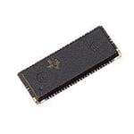
| 供应商器件封装 | 96-PBGA MICROSTAR(13.6x5.6) |
| 其它名称 | 296-17666-1 |
| 包装 | 剪切带 (CT) |
| 单位重量 | 166.600 mg |
| 商标 | Texas Instruments |
| 安装类型 | 表面贴装 |
| 安装风格 | SMD/SMT |
| 导通电阻—最大值 | 7 Ohms |
| 封装 | Reel |
| 封装/外壳 | 96-LFBGA |
| 封装/箱体 | BGA-96 Microstar |
| 工作温度 | -40°C ~ 85°C |
| 工厂包装数量 | 1000 |
| 开关数量 | 8 |
| 技术 | CB3Q |
| 最大工作温度 | + 85 C |
| 最小工作温度 | - 40 C |
| 标准包装 | 1 |
| 独立电路 | 4 |
| 电压-电源 | 2.3 V ~ 3.6 V |
| 电压源 | 单电源 |
| 电流-输出高,低 | - |
| 电源电压-最大 | 3.6 V |
| 电源电压-最小 | 2.3 V |
| 电源电流 | 20 mA |
| 电路 | 8 x 1:1 |
| 类型 | FET 总线开关 |
| 系列 | SN74CB3Q32245 |
| 逻辑系列 | CB3Q |


.jpg)


- 商务部:美国ITC正式对集成电路等产品启动337调查
- 曝三星4nm工艺存在良率问题 高通将骁龙8 Gen1或转产台积电
- 太阳诱电将投资9.5亿元在常州建新厂生产MLCC 预计2023年完工
- 英特尔发布欧洲新工厂建设计划 深化IDM 2.0 战略
- 台积电先进制程称霸业界 有大客户加持明年业绩稳了
- 达到5530亿美元!SIA预计今年全球半导体销售额将创下新高
- 英特尔拟将自动驾驶子公司Mobileye上市 估值或超500亿美元
- 三星加码芯片和SET,合并消费电子和移动部门,撤换高东真等 CEO
- 三星电子宣布重大人事变动 还合并消费电子和移动部门
- 海关总署:前11个月进口集成电路产品价值2.52万亿元 增长14.8%


PDF Datasheet 数据手册内容提取
(cid:1)(cid:2)(cid:3)(cid:4)(cid:5)(cid:6)(cid:7)(cid:8)(cid:7)(cid:9)(cid:9)(cid:4)(cid:10) (cid:7)(cid:9)(cid:11)(cid:6)(cid:12)(cid:13) (cid:6)(cid:14)(cid:1) (cid:1)(cid:15)(cid:12)(cid:13)(cid:5)(cid:16) (cid:9)(cid:17)(cid:10)(cid:11)(cid:18)(cid:19)(cid:7)(cid:17)(cid:7)(cid:11)(cid:18) (cid:16)(cid:12)(cid:20)(cid:16) (cid:6)(cid:21)(cid:2)(cid:22)(cid:15)(cid:12)(cid:22)(cid:13)(cid:16) SCES622 – JANUARY 2005 (cid:1) (cid:1) Member of the Texas Instruments Data and Control Inputs Provide Widebus+ Family Undershoot Clamp Diodes (cid:1) (cid:1) High-Bandwidth Data Path Low Power Consumption (Up to 500 MHz†) (I = 2 mA Typical) CC (cid:1) (cid:1) 5-V-Tolerant I/Os with Device Powered Up V Operating Range From 2.3 V to 3.6 V CC or Powered Down (cid:1) Data I/Os Support 0- to 5-V Signaling (cid:1) Low and Flat ON-State Resistance (r ) Levels (0.8 V, 1.2 V, 1.5 V, 1.8 V, 2.5 V, 3.3 V, on Characteristics Over Operating Range 5 V) (ron = 5 Ω Typical) (cid:1) Control Inputs Can be Driven by TTL or (cid:1) Rail-to-Rail Switching on Data I/O Ports 5-V/3.3-V CMOS Outputs − 0- to 5-V Switching With 3.3-V V (cid:1) CC I Supports Partial-Power-Down Mode off − 0- to 3.3-V Switching With 2.5-V V CC Operation (cid:1) Bidirectional Data Flow, With Near-Zero (cid:1) Latch-Up Performance Exceeds 100 mA Per Propagation Delay JESD 78, Class II (cid:1) Low Input/Output Capacitance Minimizes (cid:1) ESD Performance Tested Per JESD 22 Loading and Signal Distortion − 2000-V Human-Body Model (C = 4 pF Typical) io(OFF) (A114-B, Class II) (cid:1) Fast Switching Frequency − 1000-V Charged-Device Model (C101) (fOE = 20 MHz Max) (cid:1) Supports Both Digital and Analog †For additional information regarding the performance Applications: PCI Interface, Differential characteristics of the CB3Q family, refer to the TI Signal Interface, Memory Interleaving, Bus application report, CBT-C, CB3T, and CB3Q Isolation, Low-Distortion Signal Gating Signal-Switch Families, literature number SCDA008. description/ordering information The SN74CB3Q32245 is a high-bandwidth FET bus switch utilizing a charge pump to elevate the gate voltage of the pass transistor, providing a low and flat ON-state resistance (r ). The low and flat ON-state resistance on allows for minimal propagation delay and supports rail-to-rail switching on the data input/output (I/O) ports. The device also features low data I/O capacitance to minimize capacitive loading and signal distortion on the data bus. Specifically designed to support high-bandwidth applications, the SN74CB3Q32245 provides an optimized interface solution ideally suited for broadband communications, networking, and data-intensive computing systems. The SN74CB3Q32245 is organized as four 8-bit bus switches with separate output-enable (1OE, 2OE, 3OE, 4OE) inputs. It can be used as four 8-bit bus switches, two 16-bit bus switches, or as one 32-bit bus switch. When OE is low, the associated 8-bit bus switch is ON and the A port is connected to the B port, allowing bidirectional data flow between ports. When OE is high, the associated 8-bit bus switch is OFF, and a high-impedance state exists between the A and B ports. ORDERING INFORMATION ORDERABLE TOP-SIDE TA PACKAGE‡ PART NUMBER MARKING LFBGA − GKE Tape and reel SN74CB3Q32245GKER −−4400°°CC ttoo 8855°°CC BBZZ224455 LFBGA − ZKE (Pb-free) Tape and reel SN74CB3Q32245ZKER ‡Package drawings, standard packing quantities, thermal data, symbolization, and PCB design guidelines are available at www.ti.com/sc/package. Please be aware that an important notice concerning availability, standard warranty, and use in critical applications of TexasInstruments semiconductor products and disclaimers thereto appears at the end of this data sheet. Widebus+ is a trademark of Texas Instruments. (cid:23)(cid:24)(cid:25)(cid:22)(cid:14)(cid:5)(cid:13)(cid:12)(cid:25)(cid:2) (cid:22)(cid:21)(cid:13)(cid:21) (cid:26)(cid:27)(cid:28)(cid:29)(cid:30)(cid:31)!"(cid:26)(cid:29)(cid:27) (cid:26)# $%(cid:30)(cid:30)&(cid:27)" !# (cid:29)(cid:28) ’%()(cid:26)$!"(cid:26)(cid:29)(cid:27) *!"&(cid:17) Copyright 2005, Texas Instruments Incorporated (cid:23)(cid:30)(cid:29)*%$"# $(cid:29)(cid:27)(cid:28)(cid:29)(cid:30)(cid:31) "(cid:29) #’&$(cid:26)(cid:28)(cid:26)$!"(cid:26)(cid:29)(cid:27)# ’&(cid:30) "+& "&(cid:30)(cid:31)# (cid:29)(cid:28) (cid:13)&,!# (cid:12)(cid:27)#"(cid:30)%(cid:31)&(cid:27)"# #"!(cid:27)*!(cid:30)* -!(cid:30)(cid:30)!(cid:27)".(cid:17) (cid:23)(cid:30)(cid:29)*%$"(cid:26)(cid:29)(cid:27) ’(cid:30)(cid:29)$&##(cid:26)(cid:27)/ *(cid:29)&# (cid:27)(cid:29)" (cid:27)&$&##!(cid:30)(cid:26)). (cid:26)(cid:27)$)%*& "&#"(cid:26)(cid:27)/ (cid:29)(cid:28) !)) ’!(cid:30)!(cid:31)&"&(cid:30)#(cid:17) POST OFFICE BOX 655303 • DALLAS, TEXAS 75265 1
(cid:1)(cid:2)(cid:3)(cid:4)(cid:5)(cid:6)(cid:7)(cid:8)(cid:7)(cid:9)(cid:9)(cid:4)(cid:10) (cid:7)(cid:9)(cid:11)(cid:6)(cid:12)(cid:13) (cid:6)(cid:14)(cid:1) (cid:1)(cid:15)(cid:12)(cid:13)(cid:5)(cid:16) (cid:9)(cid:17)(cid:10)(cid:11)(cid:18)(cid:19)(cid:7)(cid:17)(cid:7)(cid:11)(cid:18) (cid:16)(cid:12)(cid:20)(cid:16) (cid:6)(cid:21)(cid:2)(cid:22)(cid:15)(cid:12)(cid:22)(cid:13)(cid:16) SCES622 – JANUARY 2005 description/ordering information (continued) This device is fully specified for partial-power-down applications using I . The I circuitry prevents damaging off off current backflow through the device when it is powered down. The device has isolation during power off. To ensure the high-impedance state during power up or power down, OE should be tied to V through a pullup CC resistor; the minimum value of the resistor is determined by the current-sinking capability of the driver. FUNCTION TABLE (each 8-bit bus switch) IINNPPUUTT IINNPPUUTT//OOUUTTPPUUTT FFUUNNCCTTIIOONN OE A L B A port = B port H Z Disconnect GKE PACKAGE (TOP VIEW) terminal assignments 1 2 3 4 5 6 1 2 3 4 5 6 A A 1B2 1B1 NC 1OE 1A1 1A2 B B 1B4 1B3 GND GND 1A3 1A4 C C 1B6 1B5 VCC VCC 1A5 1A6 D 1B8 1B7 GND GND 1A7 1A8 D E 2B2 2B1 GND GND 2A1 2A2 E F 2B4 2B3 VCC VCC 2A3 2A4 F G 2B6 2B5 GND GND 2A5 2A6 G H 2B7 2B8 NC 2OE 2A8 2A7 H J 3B2 3B1 NC 3OE 3A1 3A2 J K 3B4 3B3 GND GND 3A3 3A4 K L 3B6 3B5 VCC VCC 3A5 3A6 L M 3B8 3B7 GND GND 3A7 3A8 M N 4B2 4B1 GND GND 4A1 4A2 N P 4B4 4B3 VCC VCC 4A3 4A4 P R 4B6 4B5 GND GND 4A5 4A6 R T 4B7 4B8 NC 4OE 4A8 4A7 NC − No internal connection T 2 POST OFFICE BOX 655303 • DALLAS, TEXAS 75265
(cid:1)(cid:2)(cid:3)(cid:4)(cid:5)(cid:6)(cid:7)(cid:8)(cid:7)(cid:9)(cid:9)(cid:4)(cid:10) (cid:7)(cid:9)(cid:11)(cid:6)(cid:12)(cid:13) (cid:6)(cid:14)(cid:1) (cid:1)(cid:15)(cid:12)(cid:13)(cid:5)(cid:16) (cid:9)(cid:17)(cid:10)(cid:11)(cid:18)(cid:19)(cid:7)(cid:17)(cid:7)(cid:11)(cid:18) (cid:16)(cid:12)(cid:20)(cid:16) (cid:6)(cid:21)(cid:2)(cid:22)(cid:15)(cid:12)(cid:22)(cid:13)(cid:16) SCES622 – JANUARY 2005 logic diagram (positive logic) A5 A2 E5 E2 1A1 SW 1B1 2A1 SW 2B1 D6 D1 H5 H2 1A8 SW 1B8 2A8 SW 2B8 A4 H4 1OE 2OE J5 J2 N5 N2 3A1 SW 3B1 4A1 SW 4B1 M6 M1 T5 T2 3A8 SW 3B8 4A8 SW 4B8 J4 T4 3OE 4OE simplified schematic, each FET switch (SW) A B VCC Charge Pump EN† †EN is the internal enable signal applied to the switch. POST OFFICE BOX 655303 • DALLAS, TEXAS 75265 3
(cid:1)(cid:2)(cid:3)(cid:4)(cid:5)(cid:6)(cid:7)(cid:8)(cid:7)(cid:9)(cid:9)(cid:4)(cid:10) (cid:7)(cid:9)(cid:11)(cid:6)(cid:12)(cid:13) (cid:6)(cid:14)(cid:1) (cid:1)(cid:15)(cid:12)(cid:13)(cid:5)(cid:16) (cid:9)(cid:17)(cid:10)(cid:11)(cid:18)(cid:19)(cid:7)(cid:17)(cid:7)(cid:11)(cid:18) (cid:16)(cid:12)(cid:20)(cid:16) (cid:6)(cid:21)(cid:2)(cid:22)(cid:15)(cid:12)(cid:22)(cid:13)(cid:16) SCES622 – JANUARY 2005 absolute maximum ratings over operating free-air temperature range (unless otherwise noted)† Supply voltage range, V . . . . . . . . . . . . . . . . . . . . . . . . . . . . . . . . . . . . . . . . . . . . . . . . . . . . . . . . . −0.5 V to 4.6 V CC Control input voltage range, V (see Notes 1 and 2) . . . . . . . . . . . . . . . . . . . . . . . . . . . . . . . . . . . −0.5 V to 7 V IN Switch I/O voltage range, VI/O (see Notes 1, 2, and 3) . . . . . . . . . . . . . . . . . . . . . . . . . . . . . . . . . . −0.5 V to 7 V Control input clamp current, IIK (VIN < 0) . . . . . . . . . . . . . . . . . . . . . . . . . . . . . . . . . . . . . . . . . . . . . . . . . . . −50 mA I/O port clamp current, II/OK (VI/O < 0) . . . . . . . . . . . . . . . . . . . . . . . . . . . . . . . . . . . . . . . . . . . . . . . . . . . . . −50 mA ON-state switch current, II/O (see Note 4) . . . . . . . . . . . . . . . . . . . . . . . . . . . . . . . . . . . . . . . . . . . . . . . . . . ±64 mA Continuous current through VCC or GND terminals . . . . . . . . . . . . . . . . . . . . . . . . . . . . . . . . . . . . . . . . . ±100 mA Package thermal impedance, θ (see Note 5) . . . . . . . . . . . . . . . . . . . . . . . . . . . . . . . . . . . . . . . . . . . . 40°C/W JA Storage temperature range, T . . . . . . . . . . . . . . . . . . . . . . . . . . . . . . . . . . . . . . . . . . . . . . . . . . . −65°C to 150°C stg †Stresses beyond those listed under “absolute maximum ratings” may cause permanent damage to the device. These are stress ratings only, and functional operation of the device at these or any other conditions beyond those indicated under “recommended operating conditions” is not implied. Exposure to absolute-maximum-rated conditions for extended periods may affect device reliability. NOTES: 1. All voltages are with respect to ground, unless otherwise specified. 2. The input and output voltage ratings may be exceeded if the input and output clamp-current ratings are observed. 3. VI and VO are used to denote specific conditions for VI/O. 4. II and IO are used to denote specific conditions for II/O. 5. The package thermal impedance is calculated in accordance with JESD 51-7. recommended operating conditions (see Note 6) MIN MAX UNIT VCC Supply voltage 2.3 3.6 V VCC = 2.3 V to 2.7 V 1.7 5.5 VVIIHH HHiigghh--lleevveell ccoonnttrrooll iinnppuutt vvoollttaaggee VV VCC = 2.7 V to 3.6 V 2 5.5 VCC = 2.3 V to 2.7 V 0 0.7 VVIILL LLooww--lleevveell ccoonnttrrooll iinnppuutt vvoollttaaggee VV VCC = 2.7 V to 3.6 V 0 0.8 VI/O Data input/output voltage 0 5.5 V TA Operating free-air temperature −40 85 °C NOTE 6: All unused control inputs of the device must be held at VCC or GND to ensure proper device operation. Refer to the TI application report, Implications of Slow or Floating CMOS Inputs, literature number SCBA004. 4 POST OFFICE BOX 655303 • DALLAS, TEXAS 75265
(cid:1)(cid:2)(cid:3)(cid:4)(cid:5)(cid:6)(cid:7)(cid:8)(cid:7)(cid:9)(cid:9)(cid:4)(cid:10) (cid:7)(cid:9)(cid:11)(cid:6)(cid:12)(cid:13) (cid:6)(cid:14)(cid:1) (cid:1)(cid:15)(cid:12)(cid:13)(cid:5)(cid:16) (cid:9)(cid:17)(cid:10)(cid:11)(cid:18)(cid:19)(cid:7)(cid:17)(cid:7)(cid:11)(cid:18) (cid:16)(cid:12)(cid:20)(cid:16) (cid:6)(cid:21)(cid:2)(cid:22)(cid:15)(cid:12)(cid:22)(cid:13)(cid:16) SCES622 – JANUARY 2005 electrical characteristics over recommended operating free-air temperature range (unless otherwise noted) PARAMETER TEST CONDITIONS MIN TYP† MAX UNIT VIK VCC = 3.6 V, II = −18 mA −1.8 V IIN Control inputs VCC = 3.6 V, VIN = 0 to 5.5 V ±1 µA IOZ‡ VCC = 3.6 V, VVIO = = 0 0, to 5.5 V, SVIwNit c=h V OCFCF ,or GND ±1 µA Ioff VCC = 0, VO = 0 to 5.5 V, VI = 0 1 µA II/O = 0, ICC VCC = 3.6 V, Switch ON or OFF, VIN = VCC or GND 2 4 mA ∆ICC§ Control inputs VCC = 3.6 V, One input at 3 V, Other inputs at VCC or GND 30 µA IICCCCDD¶¶ PiPinneepprruu ccttoonnttrrooll VCConCtr =o l 3in.6p uVt, switching atA 5 a0n%d dBu ptyo crtysc olepen, 00..1155 00..2255 MMmmHHAAzz// Cin Control inputs VCC = 3.3 V, VIN = 5.5 V, 3.3 V, or 0 3.5 5 pF Switch OFF, Cio(OFF) VCC = 3.3 V, VIN = VCC or GND, VI/O = 5.5 V, 3.3 V, or 0 4 6 pF Switch ON, Cio(ON) VCC = 3.3 V, VIN = VCC or GND, VI/O = 5.5 V, 3.3 V, or 0 10 13 pF VVCCCC == 22..33 VV,, VI = 0, IO = 30 mA 6 8 rroonn## TYP at VCC = 2.5 V VI = 1.7 V, IO = −15 mA 5 10 ΩΩ VI = 0, IO = 30 mA 6 8 VVCCCC == 33 VV VI = 2.4 V, IO = −15 mA 5 9 VIN and IIN refer to control inputs. VI, VO, II, and IO refer to data pins. †All typical values are at VCC = 3.3 V (unless otherwise noted), TA = 25°C. ‡For I/O ports, the parameter IOZ includes the input leakage current. §This is the increase in supply current for each input that is at the specified TTL voltage level, rather than VCC or GND. ¶This parameter specifies the dynamic power-supply current associated with the operating frequency of a single control input (see Figure 2). #Measured by the voltage drop between the A and B terminals at the indicated current through the switch. ON-state resistance is determined by the lower of the voltages of the two (A or B) terminals. switching characteristics over recommended operating free-air temperature range (unless otherwise noted) (see Figure 3) VCC = 2.5 V VCC = 3.3 V PPAARRAAMMEETTEERR FROM TO ± 0.2 V ± 0.3 V UUNNIITT ((IINNPPUUTT)) ((OOUUTTPPUUTT)) MIN MAX MIN MAX fOE|| OE A or B 10 20 MHz (cid:2) tpd A or B B or A 0.18 0.3 ns ten OE A or B 1.5 8 1.5 7 ns tdis OE A or B 1 8 1 7 ns ||Maximum switching frequency for control input (VO > VCC, VI = 5 V, RL ≥ 1 MΩ, CL = 0) (cid:2) The propagation delay is the calculated RC time constant of the typical ON-state resistance of the switch and the specified load capacitance, when driven by an ideal voltage source (zero output impedance). POST OFFICE BOX 655303 • DALLAS, TEXAS 75265 5
(cid:1)(cid:2)(cid:3)(cid:4)(cid:5)(cid:6)(cid:7)(cid:8)(cid:7)(cid:9)(cid:9)(cid:4)(cid:10) (cid:7)(cid:9)(cid:11)(cid:6)(cid:12)(cid:13) (cid:6)(cid:14)(cid:1) (cid:1)(cid:15)(cid:12)(cid:13)(cid:5)(cid:16) (cid:9)(cid:17)(cid:10)(cid:11)(cid:18)(cid:19)(cid:7)(cid:17)(cid:7)(cid:11)(cid:18) (cid:16)(cid:12)(cid:20)(cid:16) (cid:6)(cid:21)(cid:2)(cid:22)(cid:15)(cid:12)(cid:22)(cid:13)(cid:16) SCES622 – JANUARY 2005 16 Ω VCC = 3.3 V − 14 TA = 25°C ce 12 IO = −15 mA n a st 10 si e R 8 e at 6 St − N 4 O − 2 n o r 0 0.0 0.5 1.0 1.5 2.0 2.5 3.0 3.5 4.0 4.5 5.0 VI − V Figure 1. Typical r vs V on I 12 VCC = 3.3 V 10 TA = 25°C A and B ports Open 8 A m − 6 C C I 4 One OE Switching 2 0 0 2 4 6 8 10 12 14 16 18 20 OE Switching Frequency − MHz Figure 2. Typical I vs OE Switching Frequency CC 6 POST OFFICE BOX 655303 • DALLAS, TEXAS 75265
(cid:1)(cid:2)(cid:3)(cid:4)(cid:5)(cid:6)(cid:7)(cid:8)(cid:7)(cid:9)(cid:9)(cid:4)(cid:10) (cid:7)(cid:9)(cid:11)(cid:6)(cid:12)(cid:13) (cid:6)(cid:14)(cid:1) (cid:1)(cid:15)(cid:12)(cid:13)(cid:5)(cid:16) (cid:9)(cid:17)(cid:10)(cid:11)(cid:18)(cid:19)(cid:7)(cid:17)(cid:7)(cid:11)(cid:18) (cid:16)(cid:12)(cid:20)(cid:16) (cid:6)(cid:21)(cid:2)(cid:22)(cid:15)(cid:12)(cid:22)(cid:13)(cid:16) SCES622 – JANUARY 2005 PARAMETER MEASUREMENT INFORMATION VCC Input Generator VIN 50 Ω VG1 50 Ω TEST CIRCUIT DUT 2 × VCC Input Generator S1 VI VO RL Open 50 Ω GND VG2 50 Ω CL RL (see Note A) TEST VCC S1 RL VI CL V∆ tpd(s) 2.5 V ±0.2 V Open 500 Ω VCC or GND 30 pF 3.3 V ±0.3 V Open 500 Ω VCC or GND 50 pF tPLZ/tPZL 2.5 V ±0.2 V 2 × VCC 500 Ω GND 30 pF 0.15 V 3.3 V ±0.3 V 2 × VCC 500 Ω GND 50 pF 0.3 V tPHZ/tPZH 2.5 V ±0.2 V GND 500 Ω VCC 30 pF 0.15 V 3.3 V ±0.3 V GND 500 Ω VCC 50 pF 0.3 V Output VCC Control VCC/2 VCC/2 (VIN) 0 V tPZL tPLZ Output VCC Output VCC Waveform 1 Control VCC/2 VCC/2 S1 at 2 × VCC VCC/2 VOL + V∆ (VIN) 0 V (see Note B) VOL tPZH tPHZ tPLH tPHL Output VOH VOH Waveform 2 VOH − V∆ Output VCC/2 VCC/2 S1 at GND VCC/2 VOL (see Note B) 0 V VOLTAGE WAVEFORMS VOLTAGE WAVEFORMS PROPAGATION DELAY TIMES (tpd(s)) ENABLE AND DISABLE TIMES NOTES: A. CL includes probe and jig capacitance. B. Waveform 1 is for an output with internal conditions such that the output is low, except when disabled by the output control. Waveform 2 is for an output with internal conditions such that the output is high, except when disabled by the output control. C. All input pulses are supplied by generators having the following characteristics: PRR ≤10 MHz, ZO = 50 Ω, tr ≤2.5 ns, tf ≤2.5 ns. D. The outputs are measured one at a time, with one transition per measurement. E. tPLZ and tPHZ are the same as tdis. F. tPZL and tPZH are the same as ten. G. tPLH and tPHL are the same as tpd(s). The tpd propagation delay is the calculated RC time constant of the typical ON-state resistance of the switch and the specified load capacitance, when driven by an ideal voltage source (zero output impedance). H. All parameters and waveforms are not applicable to all devices. Figure 3. Test Circuit and Voltage Waveforms POST OFFICE BOX 655303 • DALLAS, TEXAS 75265 7
PACKAGE OPTION ADDENDUM www.ti.com 30-Dec-2019 PACKAGING INFORMATION Orderable Device Status Package Type Package Pins Package Eco Plan Lead/Ball Finish MSL Peak Temp Op Temp (°C) Device Marking Samples (1) Drawing Qty (2) (6) (3) (4/5) SN74CB3Q32245GKER LIFEBUY LFBGA GKE 96 1000 TBD SNPB Level-2-235C-1 YEAR -40 to 85 BZ245 SN74CB3Q32245ZKER LIFEBUY LFBGA ZKE 96 1000 Green (RoHS SNAGCU Level-3-260C-168 HR -40 to 85 BZ245 & no Sb/Br) (1) The marketing status values are defined as follows: ACTIVE: Product device recommended for new designs. LIFEBUY: TI has announced that the device will be discontinued, and a lifetime-buy period is in effect. NRND: Not recommended for new designs. Device is in production to support existing customers, but TI does not recommend using this part in a new design. PREVIEW: Device has been announced but is not in production. Samples may or may not be available. OBSOLETE: TI has discontinued the production of the device. (2) RoHS: TI defines "RoHS" to mean semiconductor products that are compliant with the current EU RoHS requirements for all 10 RoHS substances, including the requirement that RoHS substance do not exceed 0.1% by weight in homogeneous materials. Where designed to be soldered at high temperatures, "RoHS" products are suitable for use in specified lead-free processes. TI may reference these types of products as "Pb-Free". RoHS Exempt: TI defines "RoHS Exempt" to mean products that contain lead but are compliant with EU RoHS pursuant to a specific EU RoHS exemption. Green: TI defines "Green" to mean the content of Chlorine (Cl) and Bromine (Br) based flame retardants meet JS709B low halogen requirements of <=1000ppm threshold. Antimony trioxide based flame retardants must also meet the <=1000ppm threshold requirement. (3) MSL, Peak Temp. - The Moisture Sensitivity Level rating according to the JEDEC industry standard classifications, and peak solder temperature. (4) There may be additional marking, which relates to the logo, the lot trace code information, or the environmental category on the device. (5) Multiple Device Markings will be inside parentheses. Only one Device Marking contained in parentheses and separated by a "~" will appear on a device. If a line is indented then it is a continuation of the previous line and the two combined represent the entire Device Marking for that device. (6) Lead/Ball Finish - Orderable Devices may have multiple material finish options. Finish options are separated by a vertical ruled line. Lead/Ball Finish values may wrap to two lines if the finish value exceeds the maximum column width. Important Information and Disclaimer:The information provided on this page represents TI's knowledge and belief as of the date that it is provided. TI bases its knowledge and belief on information provided by third parties, and makes no representation or warranty as to the accuracy of such information. Efforts are underway to better integrate information from third parties. TI has taken and continues to take reasonable steps to provide representative and accurate information but may not have conducted destructive testing or chemical analysis on incoming materials and chemicals. TI and TI suppliers consider certain information to be proprietary, and thus CAS numbers and other limited information may not be available for release. In no event shall TI's liability arising out of such information exceed the total purchase price of the TI part(s) at issue in this document sold by TI to Customer on an annual basis. Addendum-Page 1
PACKAGE MATERIALS INFORMATION www.ti.com 29-Sep-2019 TAPE AND REEL INFORMATION *Alldimensionsarenominal Device Package Package Pins SPQ Reel Reel A0 B0 K0 P1 W Pin1 Type Drawing Diameter Width (mm) (mm) (mm) (mm) (mm) Quadrant (mm) W1(mm) SN74CB3Q32245GKER LFBGA GKE 96 1000 330.0 24.4 5.7 13.7 2.0 8.0 24.0 Q1 SN74CB3Q32245ZKER LFBGA ZKE 96 1000 330.0 24.4 5.7 13.7 2.0 8.0 24.0 Q1 PackMaterials-Page1
PACKAGE MATERIALS INFORMATION www.ti.com 29-Sep-2019 *Alldimensionsarenominal Device PackageType PackageDrawing Pins SPQ Length(mm) Width(mm) Height(mm) SN74CB3Q32245GKER LFBGA GKE 96 1000 336.6 336.6 41.3 SN74CB3Q32245ZKER LFBGA ZKE 96 1000 336.6 336.6 41.3 PackMaterials-Page2
None
None
IMPORTANTNOTICEANDDISCLAIMER TIPROVIDESTECHNICALANDRELIABILITYDATA(INCLUDINGDATASHEETS),DESIGNRESOURCES(INCLUDINGREFERENCE DESIGNS),APPLICATIONOROTHERDESIGNADVICE,WEBTOOLS,SAFETYINFORMATION,ANDOTHERRESOURCES“ASIS” ANDWITHALLFAULTS,ANDDISCLAIMSALLWARRANTIES,EXPRESSANDIMPLIED,INCLUDINGWITHOUTLIMITATIONANY IMPLIEDWARRANTIESOFMERCHANTABILITY,FITNESSFORAPARTICULARPURPOSEORNON-INFRINGEMENTOFTHIRD PARTYINTELLECTUALPROPERTYRIGHTS. TheseresourcesareintendedforskilleddevelopersdesigningwithTIproducts.Youaresolelyresponsiblefor(1)selectingtheappropriate TIproductsforyourapplication,(2)designing,validatingandtestingyourapplication,and(3)ensuringyourapplicationmeetsapplicable standards,andanyothersafety,security,orotherrequirements.Theseresourcesaresubjecttochangewithoutnotice.TIgrantsyou permissiontousetheseresourcesonlyfordevelopmentofanapplicationthatusestheTIproductsdescribedintheresource.Other reproductionanddisplayoftheseresourcesisprohibited.NolicenseisgrantedtoanyotherTIintellectualpropertyrightortoanythird partyintellectualpropertyright.TIdisclaimsresponsibilityfor,andyouwillfullyindemnifyTIanditsrepresentativesagainst,anyclaims, damages,costs,losses,andliabilitiesarisingoutofyouruseoftheseresources. TI’sproductsareprovidedsubjecttoTI’sTermsofSale(www.ti.com/legal/termsofsale.html)orotherapplicabletermsavailableeitheron ti.comorprovidedinconjunctionwithsuchTIproducts.TI’sprovisionoftheseresourcesdoesnotexpandorotherwisealterTI’sapplicable warrantiesorwarrantydisclaimersforTIproducts. MailingAddress:TexasInstruments,PostOfficeBox655303,Dallas,Texas75265 Copyright©2019,TexasInstrumentsIncorporated