ICGOO在线商城 > 集成电路(IC) > 逻辑 - 栅极和逆变器 - 多功能,可配置 > SN74AUP1G57YFPR
 Datasheet下载
- 型号: SN74AUP1G57YFPR
- 制造商: Texas Instruments
- 库位|库存: xxxx|xxxx
- 要求:
| 数量阶梯 | 香港交货 | 国内含税 |
| +xxxx | $xxxx | ¥xxxx |
查看当月历史价格
查看今年历史价格
SN74AUP1G57YFPR产品简介:
ICGOO电子元器件商城为您提供SN74AUP1G57YFPR由Texas Instruments设计生产,在icgoo商城现货销售,并且可以通过原厂、代理商等渠道进行代购。 SN74AUP1G57YFPR价格参考¥1.26-¥3.61。Texas InstrumentsSN74AUP1G57YFPR封装/规格:逻辑 - 栅极和逆变器 - 多功能,可配置, Configurable Multiple Function Configurable 1 Circuit 3 Input 6-DSBGA。您可以下载SN74AUP1G57YFPR参考资料、Datasheet数据手册功能说明书,资料中有SN74AUP1G57YFPR 详细功能的应用电路图电压和使用方法及教程。
SN74AUP1G57YFPR 是 Texas Instruments(德州仪器)推出的一款单通道、可配置的多功能逻辑门器件,属于逻辑 - 栅极和逆变器类别。它支持多种逻辑功能配置,如与门(AND)、或门(OR)、与非门(NAND)、或非门(NOR)、异或门(XOR)和逆变器(Inverter)等,用户可通过配置选择所需逻辑功能,具有较高的灵活性。

该器件主要应用于需要低功耗、小尺寸和多功能逻辑控制的场合,适用于便携式设备、消费类电子产品、工业控制系统和通信设备等。例如:

1. 嵌入式系统:用于实现灵活的逻辑控制功能,减少PCB空间占用。
2. 电池供电设备:低功耗特性适合用于智能手表、传感器节点等。
3. 接口转换电路:可用于电平转换、信号调理和逻辑转换。
4. 测试与测量设备:提供可编程逻辑功能,便于调试和多功能切换。
5. 工业自动化:在PLC或现场设备中用于实现灵活的逻辑判断。

其采用5引脚DSF或DRL封装,适合在空间受限的设计中使用,是一款高集成度、低电压操作的逻辑器件。
| 参数 | 数值 |
| 产品目录 | 集成电路 (IC)半导体 |
| 描述 | IC GATE MULT-FUNC CONFIG 6DSBGA逻辑门 Lo-Pwr Config Mult- |
| 产品分类 | |
| 品牌 | Texas Instruments |
| 产品手册 | |
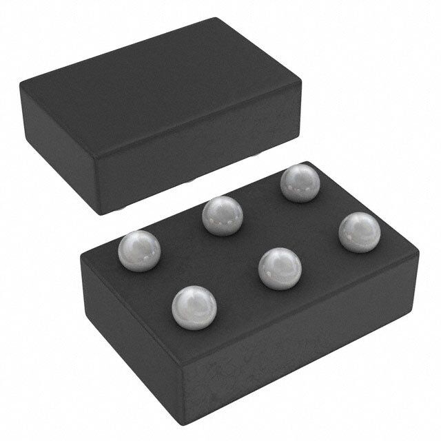
| 产品图片 |
|
| rohs | 符合RoHS无铅 / 符合限制有害物质指令(RoHS)规范要求 |
| 产品系列 | 逻辑集成电路,逻辑门,Texas Instruments SN74AUP1G57YFPR74AUP |
| 数据手册 | |
| 产品型号 | SN74AUP1G57YFPR |
| 产品 | Configurable |
| 产品目录页面 | |
| 产品种类 | 逻辑门 |
| 传播延迟时间 | 5.3 ns |
| 低电平输出电流 | 4 mA |
| 供应商器件封装 | 6-DSBGA |
| 其它名称 | 296-25396-6 |
| 包装 | Digi-Reel® |
| 商标 | Texas Instruments |
| 安装类型 | 表面贴装 |
| 安装风格 | SMD/SMT |
| 封装 | Reel |
| 封装/外壳 | 6-XFBGA,DSBGA |
| 封装/箱体 | DSBGA-6 |
| 工作温度 | -40°C ~ 85°C |
| 工作温度范围 | - 40 C to + 85 C |
| 工厂包装数量 | 3000 |
| 施密特触发器输入 | 是 |
| 最大工作温度 | + 85 C |
| 最小工作温度 | - 40 C |
| 栅极数量 | Configurable |
| 标准包装 | 1 |
| 电压-电源 | 0.8 V ~ 3.6 V |
| 电流-输出高,低 | 4mA,4mA |
| 电源电压-最大 | 3.6 V |
| 电源电压-最小 | 0.8 V |
| 电路数 | 1 |
| 系列 | SN74AUP1G57 |
| 输入/输出线数量 | 3 / 1 |
| 输入数 | 3 |
| 输入线路数量 | 3 |
| 输出电压 | 3.3 V |
| 输出电流 | 4 mA |
| 输出类型 | 单端 |
| 输出线路数量 | 1 |
| 逻辑类型 | 可配置多功能 |
| 逻辑系列 | 74AUP |
| 高电平输出电流 | - 4 mA |


- 商务部:美国ITC正式对集成电路等产品启动337调查
- 曝三星4nm工艺存在良率问题 高通将骁龙8 Gen1或转产台积电
- 太阳诱电将投资9.5亿元在常州建新厂生产MLCC 预计2023年完工
- 英特尔发布欧洲新工厂建设计划 深化IDM 2.0 战略
- 台积电先进制程称霸业界 有大客户加持明年业绩稳了
- 达到5530亿美元!SIA预计今年全球半导体销售额将创下新高
- 英特尔拟将自动驾驶子公司Mobileye上市 估值或超500亿美元
- 三星加码芯片和SET,合并消费电子和移动部门,撤换高东真等 CEO
- 三星电子宣布重大人事变动 还合并消费电子和移动部门
- 海关总署:前11个月进口集成电路产品价值2.52万亿元 增长14.8%


PDF Datasheet 数据手册内容提取
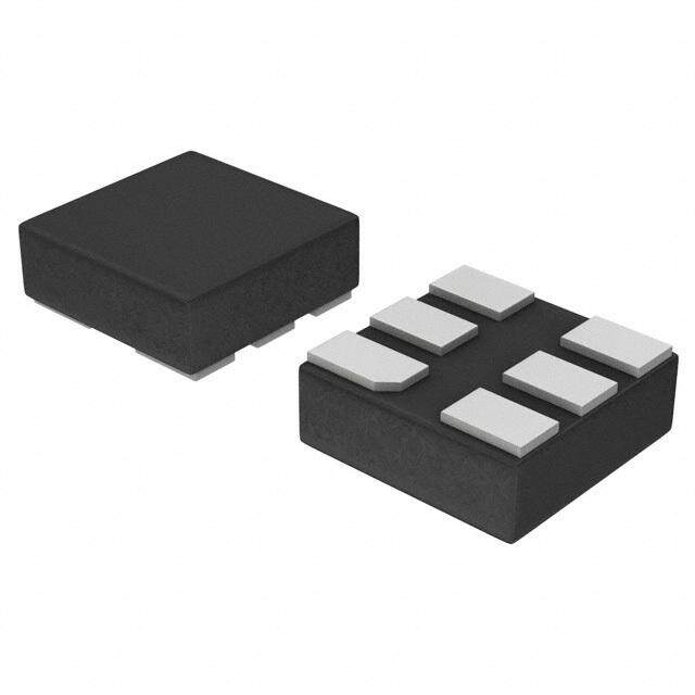
Product Sample & Technical Tools & Support & Folder Buy Documents Software Community SN74AUP1G57 SCES503J–NOVEMBER2003–REVISEDJUNE2015 SN74AUP1G57 Low-Power Configurable Multiple-Function Gate 1 Features 1 • AvailableintheTexasInstruments NanoStar™ 3 Description Packages The SN74AUP1G57 device features configurable • LowStatic-PowerConsumption multiple functions. The output state is determined by (I =0.9μAMaximum) eight patterns of 3-bit input. The user can choose the CC logic functions AND, OR, NAND, NOR, XNOR, • LowDynamic-PowerConsumption inverter, and noninverter. All inputs can be connected (C =4.3pFTypicalat3.3V) pd toV orGND. CC • LowInputCapacitance(C =1.5pFTypical) i • LowNoise–OvershootandUndershoot DeviceInformation(1) <10%ofV PARTNUMBER PACKAGE BODYSIZE(NOM) CC • I SupportsPartial-Power-DownModeOperation SN74AUP1G57YFP DSBGA(6) 1.16x0.76mm off • IncludesSchmitt-TriggerInputs SN74AUP1G57YZP DSBGA(6) 1.388x0.888mm • WideOperatingV Rangeof0.8Vto3.6V SN74AUP1G57DRY SON(6) 1.00x1.45mm CC SN74AUP1G57DSF SON(6) 1.00x1.00mm • Optimizedfor3.3-VOperation SN74AUP1G57DBV SOT-23(6) 2.80x2.90mm • 3.6-VI/OToleranttoSupportMixed-ModeSignal SN74AUP1G57DCK SC70(6) 2.10x2.00mm Operation SN74AUP1G57DRL SOT(6) 1.60x1.60mm • t =5.3nsMaximumat3.3V pd (1) For all available packages, see the orderable addendum at • SuitableforPoint-to-PointApplications theendofthedatasheet. • Latch-UpPerformanceExceeds100mAPer JESD78,ClassII FunctionalBlockDiagram(PositiveLogic) • ESDPerformanceTestedPerJESD22 3 In0 – 2000-VHuman-BodyModel 4 (A114-B,ClassII) 1 Y In1 – 1000-VCharged-DeviceModel(C101) 6 In2 2 Applications • ActiveNoiseCancellation(ANC) • BarcodeScanners • BloodPressureMonitors • CPAPMachines • CableSolutions • E-Books • EmbeddedPCs • FieldTransmitter:TemperatureorPressure Sensors • HVAC:Heating,Ventilating,andAirConditioning • Network-AttachedStorage(NAS) • ServerMotherboardandPSU • SoftwareDefinedRadio(SDR) • TV:High-Definition(HDTV),LCD,andDigital • VideoCommunicationsSystems 1 An IMPORTANT NOTICE at the end of this data sheet addresses availability, warranty, changes, use in safety-critical applications, intellectualpropertymattersandotherimportantdisclaimers.PRODUCTIONDATA.
SN74AUP1G57 SCES503J–NOVEMBER2003–REVISEDJUNE2015 www.ti.com Table of Contents 1 Features.................................................................. 1 7.2 EnableandDisableTimes........................................9 2 Applications........................................................... 1 8 DetailedDescription............................................ 10 3 Description............................................................. 1 8.1 Overview.................................................................10 4 RevisionHistory..................................................... 2 8.2 FunctionalBlockDiagram.......................................10 8.3 FeatureDescription.................................................10 5 PinConfigurationandFunctions......................... 3 8.4 DeviceFunctionalModes........................................10 6 Specifications......................................................... 4 9 ApplicationandImplementation........................ 12 6.1 AbsoluteMaximumRatings......................................4 9.1 ApplicationInformation............................................12 6.2 ESDRatings..............................................................4 9.2 TypicalApplication .................................................12 6.3 RecommendedOperatingConditions.......................4 10 PowerSupplyRecommendations..................... 13 6.4 ThermalInformation..................................................5 6.5 ElectricalCharacteristics...........................................5 11 Layout................................................................... 13 6.6 SwitchingCharacteristics,C =5pF........................6 11.1 LayoutGuidelines.................................................13 L 6.7 SwitchingCharacteristics,C =10pF......................6 11.2 LayoutExample....................................................14 L 6.8 SwitchingCharacteristics,C =15pF......................6 12 DeviceandDocumentationSupport................. 14 L 6.9 SwitchingCharacteristics,C =30pF......................7 12.1 CommunityResources..........................................14 L 6.10 OperatingCharacteristics........................................7 12.2 Trademarks...........................................................14 6.11 TypicalCharacteristics............................................7 12.3 ElectrostaticDischargeCaution............................14 7 ParameterMeasurementInformation..................8 12.4 Glossary................................................................14 7.1 PropagationDelays,SetupandHoldTimes,and 13 Mechanical,Packaging,andOrderable PulseDuration...........................................................8 Information........................................................... 14 4 Revision History ChangesfromRevisionI(May2010)toRevisionJ Page • AddedPinConfigurationandFunctionssection,ESDRatingstable,FeatureDescriptionsection,DeviceFunctional Modes,ApplicationandImplementationsection,PowerSupplyRecommendationssection,Layoutsection,Device andDocumentationSupportsection,andMechanical,Packaging,andOrderableInformationsection .............................. 1 2 SubmitDocumentationFeedback Copyright©2003–2015,TexasInstrumentsIncorporated ProductFolderLinks:SN74AUP1G57
SN74AUP1G57 www.ti.com SCES503J–NOVEMBER2003–REVISEDJUNE2015 5 Pin Configuration and Functions DBVPackage 6-PinSOT-23 DRYPackage TopView 6-PinSON TopView ln1 1 6 ln2 In1 1 6 In2 GND 2 5 V CC GND 2 5 VCC In0 3 4 Y ln0 3 4 Y DSFPackage 6-PinSON TopView DCKPackage In1 1 6 In2 6-PinSC70 TopView GND 2 5 V CC ln1 1 6 ln2 In0 3 4 Y GND 2 5 V CC YFPPackage ln0 3 4 Y 6-PinDSBGA TopView In1 A11 6A2 In2 DRLPackage 6-PinSOT GND B12 5B2 VCC TopView In0 C13 4C2 Y ln1 1 6 ln2 GND 2 5 VCC YZPPackage 6-PinDSBGA ln0 3 4 Y TopView In1 A11 6A2 In2 GND B12 5B2 VCC In0 C13 4C2 Y PinFunctions PIN SOT-23, I/O DESCRIPTION NAME DSBGA SC70,SOT ln1 1 A1 I Logicinput1 GND 2 B1 — Ground ln0 3 C1 I Logicinput0 Y 4 C2 O Logicoutput V 5 B2 — Power CC ln2 6 A2 I Logicinput2 Copyright©2003–2015,TexasInstrumentsIncorporated SubmitDocumentationFeedback 3 ProductFolderLinks:SN74AUP1G57
SN74AUP1G57 SCES503J–NOVEMBER2003–REVISEDJUNE2015 www.ti.com 6 Specifications 6.1 Absolute Maximum Ratings overoperatingfree-airtemperaturerange(unlessotherwisenoted)(1) MIN MAX UNIT V Supplyvoltage –0.5 4.6 V CC V Inputvoltage(2) –0.5 4.6 V I V Voltageappliedtoanyoutputinthehigh-impedanceorpower-offstate(2) –0.5 4.6 V O V Outputvoltageinthehighorlowstate(2) –0.5 V +0.5 V O CC I Inputclampcurrent V <0 –50 mA IK I I Outputclampcurrent V <0 –50 mA OK O I Continuousoutputcurrent ±20 mA O ContinuouscurrentthroughV orGND ±50 mA CC T Junctiontemperature 150 °C J T Storagetemperature –65 150 °C stg (1) StressesbeyondthoselistedunderAbsoluteMaximumRatingsmaycausepermanentdamagetothedevice.Thesearestressratings only,whichdonotimplyfunctionaloperationofthedeviceattheseoranyotherconditionsbeyondthoseindicatedunderRecommended OperatingConditions.Exposuretoabsolute-maximum-ratedconditionsforextendedperiodsmayaffectdevicereliability. (2) Theinputnegative-voltageandoutputvoltageratingsmaybeexceedediftheinputandoutputcurrentratingsareobserved. 6.2 ESD Ratings VALUE UNIT Human-bodymodel(HBM),perANSI/ESDA/JEDECJS-001(1) 2000 V(ESD) Electrostaticdischarge Charged-devicemodel(CDM),perJEDECspecificationJESD22- V C101(2) 1000 (1) JEDECdocumentJEP155statesthat500-VHBMallowssafemanufacturingwithastandardESDcontrolprocess. (2) JEDECdocumentJEP157statesthat250-VCDMallowssafemanufacturingwithastandardESDcontrolprocess. 6.3 Recommended Operating Conditions overoperatingfree-airtemperaturerange(unlessotherwisenoted)(1) MIN MAX UNIT V Supplyvoltage 0.8 3.6 V CC V Inputvoltage 0 3.6 V I V Outputvoltage 0 V V O CC V =0.8V –20 μA CC V =1.1V –1.1 CC V =1.4V –1.7 CC I High-leveloutputcurrent OH V =1.65 –1.9 mA CC V =2.3V –3.1 CC V =3V –4 CC V =0.8V 20 μA CC V =1.1V 1.1 CC V =1.4V 1.7 CC I Low-leveloutputcurrent OL V =1.65V 1.9 mA CC V =2.3V 3.1 CC V =3V 4 CC T Operatingfree-airtemperature –40 85 °C A (1) AllunusedinputsofthedevicemustbeheldatV orGNDtoensureproperdeviceoperation.SeetheTIapplicationreportImplications CC ofSloworFloatingCMOSInputs,SCBA004. 4 SubmitDocumentationFeedback Copyright©2003–2015,TexasInstrumentsIncorporated ProductFolderLinks:SN74AUP1G57
SN74AUP1G57 www.ti.com SCES503J–NOVEMBER2003–REVISEDJUNE2015 6.4 Thermal Information SN74AUP1G57 THERMALMETRIC(1) DBV DCK DRL DSF DRY YFP/YZP UNIT (SOT-23) (SC70) (SOT) (SON) (SON) (DSBGA) 6PINS 6PINS 6PINS 6PINS 6PINS 6PINS R Junction-to-ambientthermalresistance 165 259 142 300 234 123 °C/W θJA (1) Formoreinformationabouttraditionalandnewthermalmetrics,seetheSemiconductorandICPackageThermalMetricsapplication report,SPRA953. 6.5 Electrical Characteristics overoperatingfree-airtemperaturerange(unlessotherwisenoted) T =25°C T =–40°Cto85°C A A PARAMETER TESTCONDITIONS V UNIT CC MIN TYP MAX MIN MAX 0.8V 0.3 0.6 0.3 0.6 1.1V 0.53 0.9 0.53 0.9 V T+ Positive-going 1.4V 0.74 1.11 0.74 1.11 V inputthreshold 1.65V 0.91 1.29 0.91 1.29 voltage 2.3V 1.37 1.77 1.37 1.77 3V 1.88 2.29 1.88 2.29 0.8V 0.1 0.6 0.1 0.6 1.1V 0.26 0.65 0.26 0.65 V T- Negative-going 1.4V 0.39 0.75 0.39 0.75 V inputthreshold 1.65V 0.47 0.84 0.47 0.84 voltage 2.3V 0.69 1.04 0.69 1.04 3V 0.88 1.24 0.88 1.24 0.8V 0.07 0.5 0.07 0.5 1.1V 0.08 0.46 0.08 0.46 ΔVT 1.4V 0.18 0.56 0.18 0.56 Hysteresis V (V –V ) 1.65V 0.27 0.66 0.27 0.66 T+ T– 2.3V 0.53 0.92 0.53 0.92 3V 0.79 1.31 0.79 1.31 I =–20μA 0.8Vto3.6V V –0.1 V –0.1 OH CC CC I =–1.1mA 1.1V 0.75×V 0.7×V OH CC CC I =–1.7mA 1.4V 1.11 1.03 OH I =–1.9mA 1.65V 1.32 1.3 OH V V OH I =–2.3mA 2.05 1.97 OH 2.3V I =–3.1mA 1.9 1.85 OH I =–2.7mA 2.72 2.67 OH 3V I =–4mA 2.6 2.55 OH I =20μA 0.8Vto3.6V 0.1 0.1 OL 0.3× I =1.1mA 1.1V 0.3×V OL V CC CC I =1.7mA 1.4V 0.31 0.37 OL VOL IOL=1.9mA 1.65V 0.31 0.35 V I =2.3mA 0.31 0.33 OL 2.3V I =3.1mA 0.44 0.45 OL I =2.7mA 0.31 0.33 OL 3V I =4mA 0.44 0.45 OL I (allinputs) V =GNDto3.6V 0Vto3.6V 0.1 0.5 μA I I I V orV =0Vto3.6V 0V 0.2 0.6 μA off I O Copyright©2003–2015,TexasInstrumentsIncorporated SubmitDocumentationFeedback 5 ProductFolderLinks:SN74AUP1G57
SN74AUP1G57 SCES503J–NOVEMBER2003–REVISEDJUNE2015 www.ti.com Electrical Characteristics (continued) overoperatingfree-airtemperaturerange(unlessotherwisenoted) T =25°C T =–40°Cto85°C A A PARAMETER TESTCONDITIONS V UNIT CC MIN TYP MAX MIN MAX ΔI V orV =0Vto3.6V 0Vto0.2V 0.2 0.6 μA off I O I V =GNDor(V to3.6V), I =0 0.8Vto3.6V 0.5 0.9 μA CC I CC O ΔI V =V –0.6V(1), I =0 3.3V 40 50 μA CC I CC O 0V 1.5 C V =V orGND pF i I CC 3.6V 1.5 C V =GND 0V 3 pF o O (1) OneinputatV –0.6V,otherinputsatV orGND. CC CC 6.6 Switching Characteristics, C = 5 pF L overrecommendedoperatingfree-airtemperaturerange,C =5pF(unlessotherwisenoted)(seeFigure2andFigure3) L FROM TO TA=25°C TA=–40°Cto85°C PARAMETER V UNIT (INPUT) (OUTPUT) CC MIN TYP MAX MIN MAX 0.8V 28.6 1.2V±0.1V 2.6 9.5 13.6 2.1 17.1 1.5V±0.1V 1.9 6.4 9.1 1.4 11.1 t In0,In1,orIn2 Y ns pd 1.8V±0.15V 1.4 5.2 7.1 0.9 8.9 2.5V±0.2V 1.1 3.6 5.3 0.6 6.3 3.3V±0.3V 1 2.9 4.4 0.5 5.3 6.7 Switching Characteristics, C = 10 pF L overrecommendedoperatingfree-airtemperaturerange,C =10pF(unlessotherwisenoted)(seeFigure2andFigure3) L FROM TO TA=25°C TA=–40°Cto85°C PARAMETER V UNIT (INPUT) (OUTPUT) CC MIN TYP MAX MIN MAX 0.8V 32.8 1.2V±0.1V 2.6 11 15.1 2.1 18.1 1.5V±0.1V 1.9 7.4 10.3 1.4 12.4 t In0,In1,orIn2 Y ns pd 1.8V±0.15V 1.4 6 8.1 0.9 10 2.5V±0.2V 1.1 4.3 6.1 0.6 7.3 3.3V±0.3V 1 3.5 5.1 0.5 6.1 6.8 Switching Characteristics, C = 15 pF L overrecommendedoperatingfree-airtemperaturerange,C =15pF(unlessotherwisenoted)(seeFigure2andFigure3) L FROM TO TA=25°C TA=–40°Cto85°C PARAMETER V UNIT (INPUT) (OUTPUT) CC MIN TYP MAX MIN MAX 0.8V 37 1.2V±0.1V 3.6 12.3 16.8 3.1 20.1 1.5V±0.1V 2.8 8.3 11.4 2.3 13.7 t In0,In1,orIn2 Y ns pd 1.8V±0.15V 2.1 6.7 9 1.6 11.1 2.5V±0.2V 1.7 4.9 6.8 1.2 8.1 3.3V±0.3V 1.5 3.9 5.6 1 6.7 6 SubmitDocumentationFeedback Copyright©2003–2015,TexasInstrumentsIncorporated ProductFolderLinks:SN74AUP1G57
SN74AUP1G57 www.ti.com SCES503J–NOVEMBER2003–REVISEDJUNE2015 6.9 Switching Characteristics, C = 30 pF L overrecommendedoperatingfree-airtemperaturerange,C =30pF(unlessotherwisenoted)(seeFigure2andFigure3) L FROM TO TA=25°C TA=–40°Cto85°C PARAMETER V UNIT (INPUT) (OUTPUT) CC MIN TYP MAX MIN MAX 0.8V 49.3 1.2V±0.1V 5 15.7 21.4 4.5 26.5 1.5V±0.1V 3.9 10.8 14.4 3.4 17.4 t In0,In1,orIn2 Y ns pd 1.8V±0.15V 3.1 8.8 11.4 2.6 14 2.5V±0.2V 2.6 6.4 8.4 2.1 10.1 3.3V±0.3V 2.3 5.3 7 1.8 8.4 6.10 Operating Characteristics T =25°C A PARAMETER TESTCONDITIONS V TYP UNIT CC 0.8V 4 1.2V±0.1V 4 1.5V±0.1V 4 C Powerdissipationcapacitance f=10MHz pF pd 1.8V±0.15V 4 2.5V±0.2V 4.1 3.3V±0.3V 4.3 6.11 Typical Characteristics 40 35 30 25 s) t (npd20 15 10 5 0 0 1 2 3 4 V (V) CC C001 Figure1.t vsV ,15-pFLoad pd CC Copyright©2003–2015,TexasInstrumentsIncorporated SubmitDocumentationFeedback 7 ProductFolderLinks:SN74AUP1G57
SN74AUP1G57 SCES503J–NOVEMBER2003–REVISEDJUNE2015 www.ti.com 7 Parameter Measurement Information 7.1 Propagation Delays, Setup and Hold Times, and Pulse Duration From Output Under Test CL 1 MW (see Note A) LOAD CIRCUIT VCC = 0.8 V VC±C 0=. 11 .V2 V VC±C 0=. 11 .V5 V VC±C 0 =.1 15. 8V V VC±C 0=. 22 .V5 V VC±C 0=. 33 .V3 V CL 5, 10, 15, 30 pF 5, 10, 15, 30 pF 5, 10, 15, 30 pF 5, 10, 15, 30 pF 5, 10, 15, 30 pF 5, 10, 15, 30 pF VM VCC/2 VCC/2 VCC/2 VCC/2 VCC/2 VCC/2 VI VCC VCC VCC VCC VCC VCC tw VCC Input VCC/2 VCC/2 VI 0 V Input VM VM 0 V VOLTAGE WAVEFORMS PULSE DURATION tPLH tPHL Output VM VM VOH VCC VOL Timing Input VCC/2 0 V tPHL tPLH VOH tsu th Output VM VM VCC VOL Data Input VCC/2 VCC/2 0 V VOLTAGE WAVEFORMS PROPAGATION DELAY TIMES VOLTAGE WAVEFORMS INVERTING AND NONINVERTING OUTPUTS SETUP AND HOLD TIMES NOTES: A. CL includes probe and jig capacitance. B. All input pulses are supplied by generators having the following characteristics: PRR ≤ 10 MHz, ZO = 50 W , slew rate ≥ 1 V/ns. C. The outputs are measured one at a time, with one transition per measurement. D. tPLH and tPHL are the same as tpd. E. All parameters and waveforms are not applicable to all devices. Figure2. LoadCircuitandVoltageWaveforms 8 SubmitDocumentationFeedback Copyright©2003–2015,TexasInstrumentsIncorporated ProductFolderLinks:SN74AUP1G57
SN74AUP1G57 www.ti.com SCES503J–NOVEMBER2003–REVISEDJUNE2015 7.2 Enable and Disable Times 2 × VCC 5 kW S1 From Output Under Test GND TEST S1 CL 5 kW tPLZ/tPZL 2 × VCC (see Note A) tPHZ/tPZH GND LOAD CIRCUIT VCC = 0.8 V VC±C 0=. 11 .V2 V VC±C 0=. 11 .V5 V VC±C 0 =.1 15. 8V V VC±C 0=. 22 .V5 V VC±C 0=. 33 .V3 V CL 5, 10, 15, 30 pF 5, 10, 15, 30 pF 5, 10, 15, 30 pF 5, 10, 15, 30 pF 5, 10, 15, 30 pF 5, 10, 15, 30 pF VM VCC/2 VCC/2 VCC/2 VCC/2 VCC/2 VCC/2 VI VCC VCC VCC VCC VCC VCC VD 0.1 V 0.1 V 0.1 V 0.15 V 0.15 V 0.3 V VCC Output Control VCC/2 VCC/2 0 V tPZL tPLZ Output Waveform 1 VCC S1 at 2 × VCC VCC/2 VOL + VD (see Note B) VOL tPZH tPHZ Output WSa1v eafto GrmN D2 VCC/2 VOH - VD VOH ≈0 V (see Note B) VOLTAGE WAVEFORMS ENABLE AND DISABLE TIMES LOW- AND HIGH-LEVEL ENABLING NOTES: A. CL includes probe and jig capacitance. B. Waveform 1 is for an output with internal conditions such that the output is low, except when disabled by the output control. Waveform2 is for an output with internal conditions such that the output is high, except when disabled by the output control. C. All input pulses are supplied by generators having the following characteristics: PRR ≤ 10 MHz, ZO = 50 W , slew rate ≥ 1 V/ns. D. The outputs are measured one at a time, with one transition per measurement. E. tPLZ and tPHZ are the same as tdis. F. tPZL and tPZH are the same as ten. G. All parameters and waveforms are not applicable to all devices. Figure3. LoadCircuitandVoltageWaveforms Copyright©2003–2015,TexasInstrumentsIncorporated SubmitDocumentationFeedback 9 ProductFolderLinks:SN74AUP1G57
SN74AUP1G57 SCES503J–NOVEMBER2003–REVISEDJUNE2015 www.ti.com 8 Detailed Description 8.1 Overview The AUP family is TI's premier solution to the low-power needs of the industry in battery-powered portable applications. This family ensures a very low static and dynamic power consumption across the entire V range CC of 0.8 V to 3.6 V, resulting in an increased battery life. This product also maintains excellent signal integrity, whichproducesverylowundershootandovershootcharacteristics. The SN74AUP1G57 features configurable multiple functions. The output state is determined by eight patterns of 3-bit input. The user can choose the logic functions AND, OR, NAND, NOR, XNOR, inverter, and noninverter. All inputscanbeconnectedtoV orGND. CC The device functions as an independent gate with Schmitt-trigger inputs, which allow for slow input transition and betterswitchingnoiseimmunityattheinput. NanoStarpackagetechnologyisamajorbreakthroughinICpackagingconcepts,usingthedieasthepackage. This device is fully specified for partial-power-down applications using I . The I circuitry disables the outputs, off off preventingdamagingcurrentbackflowthroughthedevicewhenitispowereddown. 8.2 Functional Block Diagram 3 In0 4 1 Y In1 6 In2 8.3 Feature Description This part is available in the TI NanoStar package. It has low static-power consumption with I = 0.9 μA CC maximumandlowdynamicpowerconsumption(C =4.3pF,Typicalat3.3V). pd Theinputshavelowcapacitance,withtypicalC =1.5pF. i Thisparthaslownoise,withovershootandundershootlessthan10%ofV . CC This part supports partial-power-down mode operation. When this part is powered down (V = 0 V), the leakage CC currentintothedeviceischaracterizedbyI . off Schmitt-triggerinputsprovidehysterisisandconsistencyinV /V . IH IL IthasawideoperatingV rangeof0.8Vto3.6V,andhasbeenoptimizedfor3.3-Voperation. CC 3.6-VI/Otoleranttosupportmixed-modesignaloperation. Ithasalowpropagationdelayof5.3nsat3.3V. Itissuitableforpoint-to-pointapplications. 8.4 Device Functional Modes Table1listsallthefunctionalmodesoftheSN74AUP1G57. Table1.FunctionTable INPUTS OUTPUT In2 In1 In0 Y L L L H L L H L L H L H 10 SubmitDocumentationFeedback Copyright©2003–2015,TexasInstrumentsIncorporated ProductFolderLinks:SN74AUP1G57
SN74AUP1G57 www.ti.com SCES503J–NOVEMBER2003–REVISEDJUNE2015 Table1.FunctionTable(continued) INPUTS OUTPUT In2 In1 In0 Y L H H L H L L L H L H L H H L H H H H H 8.4.1 LogicConfigurations Table2listsallthelogicfunctionsoftheSN74AUP1G57. Table2.FunctionSelectionTable LOGICFUNCTION FIGURENO. 2-inputAND Figure4 2-inputANDwithbothinputsinverted Figure7 2-inputNANDwithinvertedinput Figure5,Figure6 2-inputORwithinvertedinput Figure5,Figure6 2-inputNOR Figure7 2-inputNORwithbothinputsinverted Figure4 2-inputXNOR Figure8 V V CC CC A A Y Y B B A 1 6 B A 1 6 B A 2 5 A 2 5 Y Y 3 4 Y 3 4 Y B B Figure4.2-InputANDGate Figure5.2-InputNANDGateWithInvertedAInput VCC VCC A A Y Y B B 1 6 B 1 6 B A Y A 23 54 Y AB Y A 23 54 Y B Figure7.2-InputNORGate Figure6.2-InputNANDGateWithInvertedBInput V CC A A 1 6 B Y B 2 5 3 4 Y Figure8.2-InputXNORGate Copyright©2003–2015,TexasInstrumentsIncorporated SubmitDocumentationFeedback 11 ProductFolderLinks:SN74AUP1G57
SN74AUP1G57 SCES503J–NOVEMBER2003–REVISEDJUNE2015 www.ti.com 9 Application and Implementation NOTE Information in the following applications sections is not part of the TI component specification, and TI does not warrant its accuracy or completeness. TI’s customers are responsible for determining suitability of components for their purposes. Customers should validateandtesttheirdesignimplementationtoconfirmsystemfunctionality. 9.1 Application Information The SN74AUP1G57 features configurable multiple functions. The output state is determined by eight patterns of 3-bit input. The user can choose the logic functions AND, NAND, NOR, XNOR, inverter, and noninverter. All inputscanbeconnectedtoV orGND. CC This part can be used in any application where an equivalent single gate would work. The biggest benefit to this part is that it can be used for multiple functions on the same board, reducing the total number of part numbers to beused. 9.2 Typical Application This application shows how the SN74AUP1G57 can be configured to work as an AND logic gate. This part can Thecapacitorshownis0.1uFandshouldbeplacedascloseaspossibletothepart. V CC B 1 ln1 ln2 6 C V CC 2 GND V 5 Y CC V CC 3 ln0 Y 4 A SN74AUP1G57 Figure9. SchematicforANDGateConfigurationofSN74AUP1G57 9.2.1 DesignRequirements ThisdeviceusesCMOStechnologyandhasbalancedoutputdrive.Takecaretoavoidbuscontentionbecauseit candrivecurrentsthatwouldexceedmaximumlimits. 9.2.2 DetailedDesignProcedure 1. RecommendedInputconditions – Risetimeandfalltimespecs.See(Δt/ΔV)inRecommendedOperatingConditions – Specifiedhighandlowlevels.See(V andV )inRecommendedOperatingConditions IH IL – Inputsareovervoltagetolerantallowingthemtogoashighas4.6VatanyvalidV CC 2. Recommendoutputconditions – Loadcurrentsshouldnotexceed20mAontheoutputand50mAtotalforthepart – OutputsshouldnotbepulledaboveV +0.5V. CC 12 SubmitDocumentationFeedback Copyright©2003–2015,TexasInstrumentsIncorporated ProductFolderLinks:SN74AUP1G57
SN74AUP1G57 www.ti.com SCES503J–NOVEMBER2003–REVISEDJUNE2015 Typical Application (continued) 9.2.3 ApplicationCurve The AUP family of single gate logic makes excellent translators for the new lower voltage microprocessors that typically are powered from 0.8 V to 1.2 V. They can drop the voltage of peripheral drivers and accessories that arestillpoweredby3.3Vtothenewmicrocontrollerpowerlevels. Figure10. AUP–TheLowest-PowerFamily 10 Power Supply Recommendations The power supply can be any voltage between the minimum and maximum supply voltage rating located in the RecommendedOperatingConditions. Each V terminal should have a good bypass capacitor to prevent power disturbance. For devices with a single CC supply, a 0.1-μF bypass capacitor is recommended. If there are multiple pins labeled V , then a 0.01-μF or CC 0.022-μF capacitor is recommended for each V because the V pins will be tied together internally. For CC CC devices with dual supply pins operating at different voltages, for example V and V , a 0.1-µF bypass CC DD capacitor is recommended for each supply pin. It is acceptable to parallel multiple bypass capacitors to reject different frequencies of noise. 0.1-μF and 1-μF capacitors are commonly used in parallel. The bypass capacitor shouldbeinstalledasclosetothepowerterminalaspossibleforbestresults. 11 Layout 11.1 Layout Guidelines Reflections and matching are closely related to the loop antenna theory but are different enough to be discussed separately from the theory. When a PCB trace turns a corner at a 90° angle, a reflection can occur. A reflection occurs primarily because of the change of width of the trace. At the apex of the turn, the trace width increases to 1.414 times the width. This increase upsets the transmission-line characteristics, especially the distributed capacitance and self–inductance of the trace which results in the reflection. Not all PCB traces can be straight and therefore some traces must turn corners. Figure 11 shows progressively better techniques of rounding corners.Onlythelastexample(BEST)maintainsconstanttracewidthandminimizesreflections. Copyright©2003–2015,TexasInstrumentsIncorporated SubmitDocumentationFeedback 13 ProductFolderLinks:SN74AUP1G57
SN74AUP1G57 SCES503J–NOVEMBER2003–REVISEDJUNE2015 www.ti.com 11.2 Layout Example WORST BETTER BEST W 2 1W min. W Figure11. TraceExample 12 Device and Documentation Support 12.1 Community Resources The following links connect to TI community resources. Linked contents are provided "AS IS" by the respective contributors. They do not constitute TI specifications and do not necessarily reflect TI's views; see TI's Terms of Use. TIE2E™OnlineCommunity TI'sEngineer-to-Engineer(E2E)Community.Createdtofostercollaboration amongengineers.Ate2e.ti.com,youcanaskquestions,shareknowledge,exploreideasandhelp solveproblemswithfellowengineers. DesignSupport TI'sDesignSupport QuicklyfindhelpfulE2Eforumsalongwithdesignsupporttoolsand contactinformationfortechnicalsupport. 12.2 Trademarks NanoStar,E2EaretrademarksofTexasInstruments. Allothertrademarksarethepropertyoftheirrespectiveowners. 12.3 Electrostatic Discharge Caution Thesedeviceshavelimitedbuilt-inESDprotection.Theleadsshouldbeshortedtogetherorthedeviceplacedinconductivefoam duringstorageorhandlingtopreventelectrostaticdamagetotheMOSgates. 12.4 Glossary SLYZ022—TIGlossary. Thisglossarylistsandexplainsterms,acronyms,anddefinitions. 13 Mechanical, Packaging, and Orderable Information The following pages include mechanical, packaging, and orderable information. This information is the most current data available for the designated devices. This data is subject to change without notice and revision of thisdocument.Forbrowser-basedversionsofthisdatasheet,refertotheleft-handnavigation. 14 SubmitDocumentationFeedback Copyright©2003–2015,TexasInstrumentsIncorporated ProductFolderLinks:SN74AUP1G57
PACKAGE OPTION ADDENDUM www.ti.com 6-Feb-2020 PACKAGING INFORMATION Orderable Device Status Package Type Package Pins Package Eco Plan Lead/Ball Finish MSL Peak Temp Op Temp (°C) Device Marking Samples (1) Drawing Qty (2) (6) (3) (4/5) SN74AUP1G57DBVR ACTIVE SOT-23 DBV 6 3000 Green (RoHS NIPDAU Level-1-260C-UNLIM -40 to 85 HA7R & no Sb/Br) SN74AUP1G57DBVT ACTIVE SOT-23 DBV 6 250 Green (RoHS NIPDAU Level-1-260C-UNLIM -40 to 85 HA7R & no Sb/Br) SN74AUP1G57DCKR ACTIVE SC70 DCK 6 3000 Green (RoHS NIPDAU Level-1-260C-UNLIM -40 to 85 HHR & no Sb/Br) SN74AUP1G57DCKRE4 ACTIVE SC70 DCK 6 3000 Green (RoHS NIPDAU Level-1-260C-UNLIM -40 to 85 HHR & no Sb/Br) SN74AUP1G57DCKT ACTIVE SC70 DCK 6 250 Green (RoHS NIPDAU Level-1-260C-UNLIM -40 to 85 HHR & no Sb/Br) SN74AUP1G57DRLR ACTIVE SOT-5X3 DRL 6 4000 Green (RoHS NIPDAU | NIPDAUAG Level-1-260C-UNLIM -40 to 85 (HH7, HHR) & no Sb/Br) SN74AUP1G57DRLRG4 ACTIVE SOT-5X3 DRL 6 4000 Green (RoHS NIPDAU Level-1-260C-UNLIM -40 to 85 (HH7, HHR) & no Sb/Br) SN74AUP1G57DRYR ACTIVE SON DRY 6 5000 Green (RoHS NIPDAU Level-1-260C-UNLIM -40 to 85 HH & no Sb/Br) SN74AUP1G57DSFR ACTIVE SON DSF 6 5000 Green (RoHS NIPDAU | NIPDAUAG Level-1-260C-UNLIM -40 to 85 HH & no Sb/Br) SN74AUP1G57YFPR ACTIVE DSBGA YFP 6 3000 Green (RoHS SNAGCU Level-1-260C-UNLIM HHN & no Sb/Br) SN74AUP1G57YZPR ACTIVE DSBGA YZP 6 3000 Green (RoHS SNAGCU Level-1-260C-UNLIM -40 to 85 HHN & no Sb/Br) (1) The marketing status values are defined as follows: ACTIVE: Product device recommended for new designs. LIFEBUY: TI has announced that the device will be discontinued, and a lifetime-buy period is in effect. NRND: Not recommended for new designs. Device is in production to support existing customers, but TI does not recommend using this part in a new design. PREVIEW: Device has been announced but is not in production. Samples may or may not be available. OBSOLETE: TI has discontinued the production of the device. (2) RoHS: TI defines "RoHS" to mean semiconductor products that are compliant with the current EU RoHS requirements for all 10 RoHS substances, including the requirement that RoHS substance do not exceed 0.1% by weight in homogeneous materials. Where designed to be soldered at high temperatures, "RoHS" products are suitable for use in specified lead-free processes. TI may reference these types of products as "Pb-Free". RoHS Exempt: TI defines "RoHS Exempt" to mean products that contain lead but are compliant with EU RoHS pursuant to a specific EU RoHS exemption. Green: TI defines "Green" to mean the content of Chlorine (Cl) and Bromine (Br) based flame retardants meet JS709B low halogen requirements of <=1000ppm threshold. Antimony trioxide based flame retardants must also meet the <=1000ppm threshold requirement. Addendum-Page 1
PACKAGE OPTION ADDENDUM www.ti.com 6-Feb-2020 (3) MSL, Peak Temp. - The Moisture Sensitivity Level rating according to the JEDEC industry standard classifications, and peak solder temperature. (4) There may be additional marking, which relates to the logo, the lot trace code information, or the environmental category on the device. (5) Multiple Device Markings will be inside parentheses. Only one Device Marking contained in parentheses and separated by a "~" will appear on a device. If a line is indented then it is a continuation of the previous line and the two combined represent the entire Device Marking for that device. (6) Lead/Ball Finish - Orderable Devices may have multiple material finish options. Finish options are separated by a vertical ruled line. Lead/Ball Finish values may wrap to two lines if the finish value exceeds the maximum column width. Important Information and Disclaimer:The information provided on this page represents TI's knowledge and belief as of the date that it is provided. TI bases its knowledge and belief on information provided by third parties, and makes no representation or warranty as to the accuracy of such information. Efforts are underway to better integrate information from third parties. TI has taken and continues to take reasonable steps to provide representative and accurate information but may not have conducted destructive testing or chemical analysis on incoming materials and chemicals. TI and TI suppliers consider certain information to be proprietary, and thus CAS numbers and other limited information may not be available for release. In no event shall TI's liability arising out of such information exceed the total purchase price of the TI part(s) at issue in this document sold by TI to Customer on an annual basis. Addendum-Page 2
PACKAGE MATERIALS INFORMATION www.ti.com 18-Jan-2020 TAPE AND REEL INFORMATION *Alldimensionsarenominal Device Package Package Pins SPQ Reel Reel A0 B0 K0 P1 W Pin1 Type Drawing Diameter Width (mm) (mm) (mm) (mm) (mm) Quadrant (mm) W1(mm) SN74AUP1G57DBVR SOT-23 DBV 6 3000 180.0 8.4 3.23 3.17 1.37 4.0 8.0 Q3 SN74AUP1G57DBVT SOT-23 DBV 6 250 180.0 8.4 3.23 3.17 1.37 4.0 8.0 Q3 SN74AUP1G57DCKR SC70 DCK 6 3000 180.0 8.4 2.41 2.41 1.2 4.0 8.0 Q3 SN74AUP1G57DCKT SC70 DCK 6 250 180.0 8.4 2.41 2.41 1.2 4.0 8.0 Q3 SN74AUP1G57DRLR SOT-5X3 DRL 6 4000 180.0 9.5 1.78 1.78 0.69 4.0 8.0 Q3 SN74AUP1G57DRLR SOT-5X3 DRL 6 4000 180.0 8.4 1.98 1.78 0.69 4.0 8.0 Q3 SN74AUP1G57DRYR SON DRY 6 5000 180.0 9.5 1.15 1.6 0.75 4.0 8.0 Q1 SN74AUP1G57DSFR SON DSF 6 5000 180.0 9.5 1.16 1.16 0.5 4.0 8.0 Q2 SN74AUP1G57YFPR DSBGA YFP 6 3000 178.0 9.2 0.89 1.29 0.62 4.0 8.0 Q1 SN74AUP1G57YZPR DSBGA YZP 6 3000 178.0 9.2 1.02 1.52 0.63 4.0 8.0 Q1 PackMaterials-Page1
PACKAGE MATERIALS INFORMATION www.ti.com 18-Jan-2020 *Alldimensionsarenominal Device PackageType PackageDrawing Pins SPQ Length(mm) Width(mm) Height(mm) SN74AUP1G57DBVR SOT-23 DBV 6 3000 202.0 201.0 28.0 SN74AUP1G57DBVT SOT-23 DBV 6 250 202.0 201.0 28.0 SN74AUP1G57DCKR SC70 DCK 6 3000 202.0 201.0 28.0 SN74AUP1G57DCKT SC70 DCK 6 250 202.0 201.0 28.0 SN74AUP1G57DRLR SOT-5X3 DRL 6 4000 184.0 184.0 19.0 SN74AUP1G57DRLR SOT-5X3 DRL 6 4000 202.0 201.0 28.0 SN74AUP1G57DRYR SON DRY 6 5000 184.0 184.0 19.0 SN74AUP1G57DSFR SON DSF 6 5000 184.0 184.0 19.0 SN74AUP1G57YFPR DSBGA YFP 6 3000 220.0 220.0 35.0 SN74AUP1G57YZPR DSBGA YZP 6 3000 220.0 220.0 35.0 PackMaterials-Page2
GENERIC PACKAGE VIEW DRY 6 USON - 0.6 mm max height PLASTIC SMALL OUTLINE - NO LEAD Images above are just a representation of the package family, actual package may vary. Refer to the product data sheet for package details. 4207181/G
PACKAGE OUTLINE DRY0006A USON - 0.6 mm max height SCALE 8.500 PLASTIC SMALL OUTLINE - NO LEAD B 1.05 A 0.95 PIN 1 INDEX AREA 1.5 1.4 0.6 MAX C SEATING PLANE 0.05 0.00 0.08 C 3X 0.6 SYMM (0.127) TYP (0.05) TYP 3 4 4X 0.5 SYMM 2X 1 6 1 0.25 6X 0.15 0.4 0.3 0.1 C A B 0.05 C PIN 1 ID (OPTIONAL) 0.35 5X 0.25 4222894/A 01/2018 NOTES: 1. All linear dimensions are in millimeters. Any dimensions in parenthesis are for reference only. Dimensioning and tolerancing per ASME Y14.5M. 2. This drawing is subject to change without notice. www.ti.com
EXAMPLE BOARD LAYOUT DRY0006A USON - 0.6 mm max height PLASTIC SMALL OUTLINE - NO LEAD SYMM (0.35) 5X (0.3) 1 6 6X (0.2) SYMM 4X (0.5) 4 3 (R0.05) TYP (0.6) LAND PATTERN EXAMPLE 1:1 RATIO WITH PKG SOLDER PADS EXPOSED METAL SHOWN SCALE:40X 0.05 MAX 0.05 MIN ALL AROUND ALL AROUND EXPOSED EXPOSED METAL METAL SOLDER MASK METAL METAL UNDER SOLDER MASK OPENING SOLDER MASK OPENING NON SOLDER MASK DEFINED SOLDER MASK DEFINED (PREFERRED) SOLDER MASK DETAILS 4222894/A 01/2018 NOTES: (continued) 3. For more information, see QFN/SON PCB application report in literature No. SLUA271 (www.ti.com/lit/slua271). www.ti.com
EXAMPLE STENCIL DESIGN DRY0006A USON - 0.6 mm max height PLASTIC SMALL OUTLINE - NO LEAD SYMM (0.35) 5X (0.3) 1 6 6X (0.2) SYMM 4X (0.5) 4 3 (R0.05) TYP (0.6) SOLDER PASTE EXAMPLE BASED ON 0.075 - 0.1 mm THICK STENCIL SCALE:40X 4222894/A 01/2018 NOTES: (continued) 4. Laser cutting apertures with trapezoidal walls and rounded corners may offer better paste release. IPC-7525 may have alternate design recommendations. www.ti.com
PACKAGE OUTLINE DBV0006A SOT-23 - 1.45 mm max height SCALE 4.000 SMALL OUTLINE TRANSISTOR C 3.0 2.6 0.1 C 1.75 1.45 B A 1.45 MAX PIN 1 INDEX AREA 1 6 2X 0.95 3.05 2.75 1.9 5 2 4 3 0.50 6X 0.25 0.15 0.2 C A B (1.1) TYP 0.00 0.25 GAGE PLANE 0.22 TYP 0.08 8 TYP 0.6 0 0.3 TYP SEATING PLANE 4214840/B 03/2018 NOTES: 1. All linear dimensions are in millimeters. Any dimensions in parenthesis are for reference only. Dimensioning and tolerancing per ASME Y14.5M. 2. This drawing is subject to change without notice. 3. Body dimensions do not include mold flash or protrusion. Mold flash and protrusion shall not exceed 0.15 per side. 4. Leads 1,2,3 may be wider than leads 4,5,6 for package orientation. 5. Refernce JEDEC MO-178. www.ti.com
EXAMPLE BOARD LAYOUT DBV0006A SOT-23 - 1.45 mm max height SMALL OUTLINE TRANSISTOR PKG 6X (1.1) 1 6X (0.6) 6 SYMM 2 5 2X (0.95) 3 4 (R0.05) TYP (2.6) LAND PATTERN EXAMPLE EXPOSED METAL SHOWN SCALE:15X SOLDER MASK SOLDER MASK METAL UNDER METAL OPENING OPENING SOLDER MASK EXPOSED METAL EXPOSED METAL 0.07 MAX 0.07 MIN ARROUND ARROUND NON SOLDER MASK SOLDER MASK DEFINED DEFINED (PREFERRED) SOLDER MASK DETAILS 4214840/B 03/2018 NOTES: (continued) 6. Publication IPC-7351 may have alternate designs. 7. Solder mask tolerances between and around signal pads can vary based on board fabrication site. www.ti.com
EXAMPLE STENCIL DESIGN DBV0006A SOT-23 - 1.45 mm max height SMALL OUTLINE TRANSISTOR PKG 6X (1.1) 1 6X (0.6) 6 SYMM 2 5 2X(0.95) 3 4 (R0.05) TYP (2.6) SOLDER PASTE EXAMPLE BASED ON 0.125 mm THICK STENCIL SCALE:15X 4214840/B 03/2018 NOTES: (continued) 8. Laser cutting apertures with trapezoidal walls and rounded corners may offer better paste release. IPC-7525 may have alternate design recommendations. 9. Board assembly site may have different recommendations for stencil design. www.ti.com
None
None
PACKAGE OUTLINE DRL0006A SOT - 0.6 mm max height SCALE 8.000 PLASTIC SMALL OUTLINE 1.7 1.5 PIN 1 A ID AREA 1 6 4X 0.5 1.7 1.5 2X 1 NOTE 3 4 3 B 11..31 6X 00..31 00..0050 TYP 0.6 MAX C SEATING PLANE 0.18 6X 0.08 SYMM 0.05 C SYMM 0.27 6X 0.15 0.1 C A B 0.4 6X 0.2 0.05 4223266/A 09/2016 NOTES: 1. All linear dimensions are in millimeters. Any dimensions in parenthesis are for reference only. Dimensioning and tolerancing per ASME Y14.5M. 2. This drawing is subject to change without notice. 3. This dimension does not include mold flash, protrusions, or gate burrs. Mold flash, protrusions, or gate burrs shall not exceed 0.15 mm per side. www.ti.com
EXAMPLE BOARD LAYOUT DRL0006A SOT - 0.6 mm max height PLASTIC SMALL OUTLINE 6X (0.67) SYMM 1 6X (0.3) 6 SYMM 4X (0.5) 4 3 (R0.05) TYP (1.48) LAND PATTERN EXAMPLE SCALE:30X 0.05 MAX 0.05 MIN AROUND AROUND SOLDER MASK METAL METAL UNDER SOLDER MASK OPENING SOLDER MASK OPENING NON SOLDER MASK SOLDER MASK DEFINED DEFINED (PREFERRED) SOLDERMASK DETAILS 4223266/A 09/2016 NOTES: (continued) 4. Publication IPC-7351 may have alternate designs. 5. Solder mask tolerances between and around signal pads can vary based on board fabrication site. www.ti.com
EXAMPLE STENCIL DESIGN DRL0006A SOT - 0.6 mm max height PLASTIC SMALL OUTLINE 6X (0.67) SYMM 1 6X (0.3) 6 SYMM 4X (0.5) 4 3 (R0.05) TYP (1.48) SOLDER PASTE EXAMPLE BASED ON 0.1 mm THICK STENCIL SCALE:30X 4223266/A 09/2016 NOTES: (continued) 6. Laser cutting apertures with trapezoidal walls and rounded corners may offer better paste release. IPC-7525 may have alternate design recommendations. 7. Board assembly site may have different recommendations for stencil design. www.ti.com
PACKAGE OUTLINE YFP0006 DSBGA - 0.5 mm max height SCALE 10.000 DIE SIZE BALL GRID ARRAY B E A BALL A1 CORNER D C 0.5 MAX SEATING PLANE 0.19 0.13 BALL TYP 0.05 C 0.4 TYP SYMM C D: Max = 1.19 mm, Min = 1.13 mm 0.8 TYP B SYMM E: Max = 0.79 mm, Min = 0.73 mm 0.4 TYP A 0.25 6X 0.21 1 2 0.015 C A B 4223410/A 11/2016 NOTES: 1. All linear dimensions are in millimeters. Any dimensions in parenthesis are for reference only. Dimensioning and tolerancing per ASME Y14.5M. 2. This drawing is subject to change without notice. www.ti.com
EXAMPLE BOARD LAYOUT YFP0006 DSBGA - 0.5 mm max height DIE SIZE BALL GRID ARRAY (0.4) TYP 6X ( 0.23) 1 2 A (0.4) TYP B SYMM C SYMM LAND PATTERN EXAMPLE SCALE:50X ( 0.23) 0.05 MAX 0.05 MIN METAL UNDER METAL SOLDER MASK SOLDER MASK ( 0.23) OPENING SOLDER MASK OPENING NON-SOLDER MASK SOLDER MASK DEFINED DEFINED (PREFERRED) SOLDER MASK DETAILS NOT TO SCALE 4223410/A 11/2016 NOTES: (continued) 3. Final dimensions may vary due to manufacturing tolerance considerations and also routing constraints. For more information, see Texas Instruments literature number SNVA009 (www.ti.com/lit/snva009). www.ti.com
EXAMPLE STENCIL DESIGN YFP0006 DSBGA - 0.5 mm max height DIE SIZE BALL GRID ARRAY (0.4) TYP 6X ( 0.25) (R0.05) TYP 1 2 A (0.4) TYP B SYMM METAL TYP C SYMM SOLDER PASTE EXAMPLE BASED ON 0.1 mm THICK STENCIL SCALE:50X 4223410/A 11/2016 NOTES: (continued) 4. Laser cutting apertures with trapezoidal walls and rounded corners may offer better paste release. www.ti.com
PACKAGE OUTLINE DSF0006A X2SON - 0.4 mm max height SCALE 10.000 PLASTIC SMALL OUTLINE - NO LEAD 1.05 B A 0.95 PIN 1 INDEX AREA 1.05 0.95 0.4 MAX C SEATING PLANE 0.05 C (0.11) TYP SYMM 0.05 0.00 3 4 2X SYMM 0.7 4X 0.35 6 1 0.22 6X 0.12 (0.1) PIN 1 ID 0.45 0.07 C B A 6X 0.35 0.05 C 4220597/A 06/2017 NOTES: 1. All linear dimensions are in millimeters. Any dimensions in parenthesis are for reference only. Dimensioning and tolerancing per ASME Y14.5M. 2. This drawing is subject to change without notice. 3. Reference JEDEC registration MO-287, variation X2AAF. www.ti.com
EXAMPLE BOARD LAYOUT DSF0006A X2SON - 0.4 mm max height PLASTIC SMALL OUTLINE - NO LEAD 6X (0.6) (R0.05) TYP 1 6X (0.17) 6 SYMM 4X (0.35) 4 3 SYMM (0.8) LAND PATTERN EXAMPLE EXPOSED METAL SHOWN SCALE:40X 0.07 MIN 0.07 MAX EXPOSED METAL ALL AROUND ALL AROUND EXPOSED METAL SOLDER MASK SOLDER MASK METAL METAL UNDER OPENING OPENING SOLDER MASK NON SOLDER MASK SOLDER MASK DEFINED DEFINED SOLDER MASK DETAILS 4220597/A 06/2017 NOTES: (continued) 4. For more information, see Texas Instruments literature number SLUA271 (www.ti.com/lit/slua271). www.ti.com
EXAMPLE STENCIL DESIGN DSF0006A X2SON - 0.4 mm max height PLASTIC SMALL OUTLINE - NO LEAD 6X (0.6) (R0.05) TYP 1 6X (0.17) 6 SYMM 4X (0.35) 4 3 SYMM (0.8) SOLDER PASTE EXAMPLE BASED ON 0.125 mm THICK STENCIL PRINTED SOLDER COVERAGE BY AREA UNDER PACKAGE SCALE:40X 4220597/A 06/2017 4. Laser cutting apertures with trapezoidal walls and rounded corners may offer better paste release. IPC-7525 may have alternate design recommendations. www.ti.com
PACKAGE OUTLINE YZP0006 DSBGA - 0.5 mm max height SCALE 9.000 DIE SIZE BALL GRID ARRAY B E A BALL A1 CORNER D 0.5 MAX C SEATING PLANE 0.19 BALL TYP 0.05 C 0.15 0.5 TYP C SYMM 1 D: Max = 1.418 mm, Min =1 .358 mm B TYP 0.5 E: Max = 0.918 mm, Min =0 .858 mm TYP A 0.25 1 2 6X 0.21 SYMM 0.015 C A B 4219524/A 06/2014 NOTES: NanoFree Is a trademark of Texas Instruments. 1. All linear dimensions are in millimeters. Any dimensions in parenthesis are for reference only. Dimensioning and tolerancing per ASME Y14.5M. 2. This drawing is subject to change without notice. 3. NanoFreeTM package configuration. www.ti.com
EXAMPLE BOARD LAYOUT YZP0006 DSBGA - 0.5 mm max height DIE SIZE BALL GRID ARRAY (0.5) TYP 6X ( 0.225) 1 2 A (0.5) TYP B SYMM C SYMM LAND PATTERN EXAMPLE SCALE:40X ( 0.225) 0.05 MAX 0.05 MIN METAL METAL UNDER MASK SOLDER MASK ( 0.225) OPENING SOLDER MASK OPENING NON-SOLDER MASK DEFINED SOLDER MASK (PREFERRED) DEFINED SOLDER MASK DETAILS NOT TO SCALE 4219524/A 06/2014 NOTES: (continued) 4. Final dimensions may vary due to manufacturing tolerance considerations and also routing constraints. For more information, see Texas Instruments literature number SBVA017 (www.ti.com/lit/sbva017). www.ti.com
EXAMPLE STENCIL DESIGN YZP0006 DSBGA - 0.5 mm max height DIE SIZE BALL GRID ARRAY (0.5) TYP 6X ( 0.25) (R0.05) TYP 1 2 A (0.5) TYP B SYMM METAL TYP C SYMM SOLDER PASTE EXAMPLE BASED ON 0.1 mm THICK STENCIL SCALE:40X 4219524/A 06/2014 NOTES: (continued) 5. Laser cutting apertures with trapezoidal walls and rounded corners may offer better paste release. www.ti.com
IMPORTANTNOTICEANDDISCLAIMER TI PROVIDES TECHNICAL AND RELIABILITY DATA (INCLUDING DATASHEETS), DESIGN RESOURCES (INCLUDING REFERENCE DESIGNS), APPLICATION OR OTHER DESIGN ADVICE, WEB TOOLS, SAFETY INFORMATION, AND OTHER RESOURCES “AS IS” AND WITH ALL FAULTS, AND DISCLAIMS ALL WARRANTIES, EXPRESS AND IMPLIED, INCLUDING WITHOUT LIMITATION ANY IMPLIED WARRANTIES OF MERCHANTABILITY, FITNESS FOR A PARTICULAR PURPOSE OR NON-INFRINGEMENT OF THIRD PARTY INTELLECTUAL PROPERTY RIGHTS. These resources are intended for skilled developers designing with TI products. You are solely responsible for (1) selecting the appropriate TI products for your application, (2) designing, validating and testing your application, and (3) ensuring your application meets applicable standards, and any other safety, security, or other requirements. These resources are subject to change without notice. TI grants you permission to use these resources only for development of an application that uses the TI products described in the resource. Other reproduction and display of these resources is prohibited. No license is granted to any other TI intellectual property right or to any third party intellectual property right. TI disclaims responsibility for, and you will fully indemnify TI and its representatives against, any claims, damages, costs, losses, and liabilities arising out of your use of these resources. TI’s products are provided subject to TI’s Terms of Sale (www.ti.com/legal/termsofsale.html) or other applicable terms available either on ti.com or provided in conjunction with such TI products. TI’s provision of these resources does not expand or otherwise alter TI’s applicable warranties or warranty disclaimers for TI products. Mailing Address: Texas Instruments, Post Office Box 655303, Dallas, Texas 75265 Copyright © 2020, Texas Instruments Incorporated