ICGOO在线商城 > 集成电路(IC) > 逻辑 - 缓冲器,驱动器,接收器,收发器 > SN74ALVCH32973KR
 Datasheet下载
- 型号: SN74ALVCH32973KR
- 制造商: Texas Instruments
- 库位|库存: xxxx|xxxx
- 要求:
| 数量阶梯 | 香港交货 | 国内含税 |
| +xxxx | $xxxx | ¥xxxx |
查看当月历史价格
查看今年历史价格
SN74ALVCH32973KR产品简介:
ICGOO电子元器件商城为您提供SN74ALVCH32973KR由Texas Instruments设计生产,在icgoo商城现货销售,并且可以通过原厂、代理商等渠道进行代购。 SN74ALVCH32973KR价格参考。Texas InstrumentsSN74ALVCH32973KR封装/规格:逻辑 - 缓冲器,驱动器,接收器,收发器, Buffer, Transceiver, Non-Inverting 2 Element 8 Bit per Element 3-State Output 96-LFBGA (13.5x5.5)。您可以下载SN74ALVCH32973KR参考资料、Datasheet数据手册功能说明书,资料中有SN74ALVCH32973KR 详细功能的应用电路图电压和使用方法及教程。
SN74ALVCH32973KR 是由德州仪器(Texas Instruments)生产的一款逻辑缓冲器、驱动器、接收器和收发器。它主要用于在不同电压电平的系统之间进行信号转换和传输,特别适用于需要在低电压和高电压系统之间进行接口的应用场景。

 应用场景:

1. 通信接口:
   - SN74ALVCH32973KR 常用于各种通信接口中,例如 UART、SPI 和 I2C 等。它可以将低电压信号(如 1.8V 或 2.5V)转换为高电压信号(如 3.3V 或 5V),或者反之亦然。这使得它非常适合用于连接不同的微控制器、传感器和其他外设设备,确保信号在不同电压电平下的正确传输。

2. 嵌入式系统:
   - 在嵌入式系统中,特别是那些包含多个电压域的系统中,SN74ALVCH32973KR 可以用于实现信号的电平转换。例如,在一个系统中,某些模块可能工作在 1.8V,而其他模块工作在 3.3V,这时该器件可以确保这些模块之间的信号能够正确传递,避免因电压不匹配导致的信号失真或损坏。

3. 工业自动化:
   - 在工业自动化领域,设备通常需要在不同的电压电平下工作。SN74ALVCH32973KR 可以用于连接 PLC(可编程逻辑控制器)、传感器和执行器等设备,确保它们之间的信号传输稳定可靠。此外,它还可以用于隔离敏感电路,防止外部干扰对系统的正常运行造成影响。

4. 消费电子:
   - 在消费电子产品中,如智能手机、平板电脑和其他便携式设备中,SN74ALVCH32973KR 可以用于连接内部的不同模块,例如电源管理单元、显示驱动器和音频处理器等。通过电平转换,它可以确保这些模块之间的信号传输顺畅无误,同时降低功耗。

5. 汽车电子:
   - 在汽车电子系统中,SN74ALVCH32973KR 可以用于连接车内的各种传感器、控制器和执行器。由于汽车环境中的电压波动较大,该器件可以帮助确保信号的稳定传输,从而提高系统的可靠性和安全性。

总之,SN74ALVCH32973KR 是一款功能强大的电平转换器,广泛应用于各种需要在不同电压电平之间进行信号传输的场景中,确保系统的稳定性和可靠性。
| 参数 | 数值 |
| 产品目录 | 集成电路 (IC) |
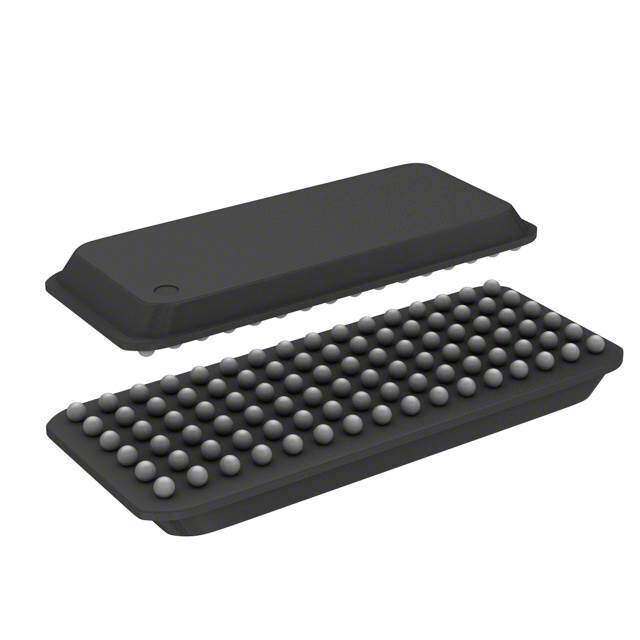
| 描述 | IC BUS TRANSCVR 16BIT 96LFBGA |
| 产品分类 | |
| 品牌 | Texas Instruments |
| 数据手册 | |
| 产品图片 |
|
| 产品型号 | SN74ALVCH32973KR |
| PCN设计/规格 | |
| rohs | 含铅 / 不符合限制有害物质指令(RoHS)规范要求 |
| 产品系列 | 74ALVCH |
| 产品目录页面 | |
| 供应商器件封装 | 96-LFBGA(13.5x5.5) |
| 元件数 | 2 |
| 其它名称 | 296-15321-1 |
| 包装 | 剪切带 (CT) |
| 安装类型 | 表面贴装 |
| 封装/外壳 | 96-LFBGA |
| 工作温度 | -40°C ~ 85°C |
| 标准包装 | 1 |
| 每元件位数 | 8 |
| 电压-电源 | 1.65 V ~ 3.6 V |
| 电流-输出高,低 | 24mA,24mA |
| 逻辑类型 | 收发器,非反相 |
.jpg)


- 商务部:美国ITC正式对集成电路等产品启动337调查
- 曝三星4nm工艺存在良率问题 高通将骁龙8 Gen1或转产台积电
- 太阳诱电将投资9.5亿元在常州建新厂生产MLCC 预计2023年完工
- 英特尔发布欧洲新工厂建设计划 深化IDM 2.0 战略
- 台积电先进制程称霸业界 有大客户加持明年业绩稳了
- 达到5530亿美元!SIA预计今年全球半导体销售额将创下新高
- 英特尔拟将自动驾驶子公司Mobileye上市 估值或超500亿美元
- 三星加码芯片和SET,合并消费电子和移动部门,撤换高东真等 CEO
- 三星电子宣布重大人事变动 还合并消费电子和移动部门
- 海关总署:前11个月进口集成电路产品价值2.52万亿元 增长14.8%


PDF Datasheet 数据手册内容提取
SN74ALVCH32973 16-BIT BUS TRANSCEIVER AND TRANSPARENT D-TYPE LATCH WITH EIGHT INDEPENDENT BUFFERS www.ti.com SCES436C–APRIL2003–REVISEDSEPTEMBER2004 FEATURES • Latch-UpPerformanceExceeds250mAPer • MemberoftheTexasInstrumentsWidebus+™ JESD17 Family • ESDProtectionExceedsJESD22 • BusHoldonDataInputsEliminatestheNeed – 2000-VHuman-BodyModel(A114-A) forExternalPullup/PulldownResistors – 200-VMachineModel(A115-A) – 1000-VCharged-DeviceModel(C101) DESCRIPTION/ORDERING INFORMATION This device contains eight independent noninverting buffers and a 16-bit noninverting bus transceiver and D-type latchdesignedfor1.65-Vto3.6-VV operation. CC The SN74ALVCH32973 is particularly suitable for demultiplexing an address/data bus into a dedicated address bus and dedicated data bus. The device is used where there is asynchronous bidirectional communication between the A and B data bus, and the address signals are latched and buffered on the Q bus. The control-functionimplementationminimizesexternaltimingrequirements. This device can be used as one 8-bit buffer, two 8-bit transceivers, and two 8-bit latches or one 8-bit buffer, one 16-bit transceiver, and one 16-bit latch. It allows data transmission from the A bus to the B bus or from the B bus to the A bus, depending on the logic level at the direction-control (DIR) input. The transceiver output-enable (TOE)inputcanbeusedtodisablethetransceiverssothattheAandBbuseseffectivelyareisolated. When the latch-enable (LE) input is high, the Q outputs follow the data (A) inputs. When LE is taken low, the Q outputsarelatchedat the levels set up at the A inputs. The latch output-enable (LOE) input can be used to place the nine Q outputs in either a normal logic state (high or low logic level) or the high-impedance state. In the high-impedance state, the Q outputs neither drive nor load the bus lines significantly. LOE does not affect internal operations of the latch. Old data can be retained or new data can be entered while the Q outputs are in thehigh-impedancestate. To ensure the high-impedance state during power up or power down, LOE and TOE should be tied to V CC through pullup resistors; the minimum values of the resistors are determined by the current-sinking capability of thedrivers. The eight independent noninverting buffers perform the Boolean function Y = D and are independent of the state ofDIR,TOE,LE,andLOE. The A and B I/Os and D inputs have bus-hold circuitry. Active bus-hold circuitry holds unused or undriven data inputsatavalidlogicstate.Useofpulluporpulldownresistorswiththebus-holdcircuitryisnotrecommended. ORDERINGINFORMATION T PACKAGE(1) ORDERABLEPARTNUMBER TOP-SIDEMARKING A LFBGA-GKE SN74ALVCH32973KR -40(cid:176) Cto85(cid:176) C Tapeandreel ACH973 LFBGA-ZKE(Pb-free) 74ALVCH32973ZKER (1) Packagedrawings,standardpackingquantities,thermaldata,symbolization,andPCBdesignguidelinesareavailableat www.ti.com/sc/package. Pleasebeawarethatanimportantnoticeconcerningavailability,standardwarranty,anduseincriticalapplicationsofTexas Instrumentssemiconductorproductsanddisclaimerstheretoappearsattheendofthisdatasheet. Widebus+isatrademarkofTexasInstruments. PRODUCTIONDATAinformationiscurrentasofpublicationdate. Copyright©2003–2004,TexasInstrumentsIncorporated Products conform to specifications per the terms of the Texas Instruments standard warranty. Production processing does not necessarilyincludetestingofallparameters.
SN74ALVCH32973 16-BIT BUS TRANSCEIVER AND TRANSPARENT D-TYPE LATCH WITH EIGHT INDEPENDENT BUFFERS www.ti.com SCES436C–APRIL2003–REVISEDSEPTEMBER2004 GKE OR ZKE PACKAGE rt (TOP VIEW) rt 1 2 3 4 5 6 TERMINALASrt SIGNMENTS 1 2 3 4 5 6 A A 1A1 D1 1TOE 1DIR 1B1 1Q1 B B 1A2 Y1 GND GND 1B2 1Q2 C C 1A3 D2 V V 1B3 1Q3 CC CC D D 1A4 Y2 GND GND 1B4 1Q4 E E 1A5 D3 GND GND 1B5 1Q5 F F 1A6 Y3 V V 1B6 1Q6 CC CC G G 1A7 D4 GND GND 1B7 1Q7 H H 1A8 Y4 1LE 1LOE 1B8 1Q8 J J 2A1 D5 2TOE 2DIR 2B1 2Q1 K K 2A2 Y5 GND GND 2B2 2Q2 L 2A3 D6 V V 2B3 2Q3 L CC CC M 2A4 Y6 GND GND 2B4 2Q4 M N 2A5 D7 GND GND 2B5 2Q5 N P 2A6 Y7 V V 2B6 2Q6 CC CC P R 2A7 D8 GND GND 2B7 2Q7 R T 2A8 Y8 2LE 2LOE 2B8 2Q8 T FUNCTIONTABLES INPUTS OPERATION TOE DIR L L BdatatoAbus L H AdatatoBbus H X AbusandBbusisolation INPUTS OUTPUT LOE LE A Q L H H H L H L L L L X Q 0 H X X Z INPUT OUTPUT D Y L L H H 2
SN74ALVCH32973 16-BIT BUS TRANSCEIVER AND TRANSPARENT D-TYPE LATCH WITH EIGHT INDEPENDENT BUFFERS www.ti.com SCES436C–APRIL2003–REVISEDSEPTEMBER2004 LOGICDIAGRAM(POSITIVELOGIC) A4 1DIR A3 1TOE H4 1LOE H3 1LE One of Eight Channels C1 A6 1Q1 1D A1 1A1 A5 1B1 To Seven Other Channels 3
SN74ALVCH32973 16-BIT BUS TRANSCEIVER AND TRANSPARENT D-TYPE LATCH WITH EIGHT INDEPENDENT BUFFERS www.ti.com SCES436C–APRIL2003–REVISEDSEPTEMBER2004 LOGICDIAGRAM(POSITIVELOGIC) 2DIR J4 J3 2TOE T4 2LOE T3 2LE One of Eight Channels C1 J6 2Q1 1D J1 2A1 J5 2B1 To Seven Other Channels One of Eight Channels A2 B2 D1 Y1 4
SN74ALVCH32973 16-BIT BUS TRANSCEIVER AND TRANSPARENT D-TYPE LATCH WITH EIGHT INDEPENDENT BUFFERS www.ti.com SCES436C–APRIL2003–REVISEDSEPTEMBER2004 ABSOLUTE MAXIMUM RATINGS(1) overoperatingfree-airtemperaturerange(unlessotherwisenoted) MIN MAX UNIT V Supplyvoltagerange -0.5 4.6 V CC ExceptI/OandDinputports(2) -0.5 4.6 V Inputvoltagerange V I I/OandDinputports(2)(3) -0.5 V +0.5 CC V Outputvoltagerange(2)(3) -0.5 V +0.5 V O CC I Inputclampcurrent V <0 -50 mA IK I I Outputclampcurrent V <0 -50 mA OK O I Continuousoutputcurrent – 50 mA O ContinuouscurrentthrougheachV orGND – 100 mA CC q Packagethermalimpedance(4) GKE/ZKEpackage 40 (cid:176) C/W JA T Storagetemperaturerange -65 150 (cid:176) C stg (1) Stressesbeyondthoselistedunder"absolutemaximumratings"maycausepermanentdamagetothedevice.Thesearestressratings only,andfunctionaloperationofthedeviceattheseoranyotherconditionsbeyondthoseindicatedunder"recommendedoperating conditions"isnotimplied.Exposuretoabsolute-maximum-ratedconditionsforextendedperiodsmayaffectdevicereliability. (2) Theinputnegative-voltageandoutputvoltageratingsmaybeexceedediftheinputandoutputcurrentratingsareobserved. (3) Thisvalueislimitedto4.6Vmaximum. (4) ThepackagethermalimpedanceiscalculatedinaccordancewithJESD51-7. RECOMMENDED OPERATING CONDITIONS(1) MIN MAX UNIT V Supplyvoltage 1.65 3.6 V CC V =1.65Vto1.95V 0.65· V CC CC V High-levelinputvoltage V =2.3Vto2.7V 1.7 V IH CC V =3Vto3.6V 2 CC V =1.65Vto1.95V 0.35· V CC CC V Low-levelinputvoltage V =2.3Vto2.7V 0.7 V IL CC V =3Vto3.6V 0.8 CC V Inputvoltage 0 V V I CC V Outputvoltage 0 V V O CC V =1.65V -4 CC V =2.3V -12 CC I High-leveloutputcurrent mA OH V =2.7V -12 CC V =3V -24 CC V =1.65V 4 CC V =2.3V 12 CC I Low-leveloutputcurrent mA OL V =2.7V 12 CC V =3V 24 CC D t/D v Inputtransitionriseorfallrate 10 ns/V T Operatingfree-airtemperature -40 85 (cid:176) C A (1) AllunusedcontrolinputsofthedevicemustbeheldatV orGNDtoensureproperdeviceoperation.RefertotheTIapplicationreport, CC ImplicationsofSloworFloatingCMOSInputs,literaturenumberSCBA004. 5
SN74ALVCH32973 16-BIT BUS TRANSCEIVER AND TRANSPARENT D-TYPE LATCH WITH EIGHT INDEPENDENT BUFFERS www.ti.com SCES436C–APRIL2003–REVISEDSEPTEMBER2004 ELECTRICAL CHARACTERISTICS overrecommendedoperatingfree-airtemperaturerange(unlessotherwisenoted) PARAMETER TESTCONDITIONS V MIN TYP(1) MAX UNIT CC I =-100m A 1.65Vto3.6V V -0.2 OH CC I =-4mA 1.65V 1.2 OH I =-6mA 2.3V 2 OH V 2.3V 1.7 V OH I =-12mA 2.7V 2.2 OH 3V 2.4 I =-24mA 3V 2 OH I =100m A 1.65Vto3.6V 0.2 OL I =4mA 1.65V 0.45 OL I =6mA 2.3V 0.4 OL V V OL 2.3V 0.7 I =12mA OL 2.7V 0.4 I =24mA 3V 0.55 OL I V =V orGND 3.6V – 5 m A I I CC V =0.57V 1.65V 25 I I (2) V =0.7V 2.3V 45 m A BHL I V =0.8V 3V 75 I V =1.07V 1.65V -25 I I (3) V =1.7V 2.3V -45 m A BHH I V =2V 3V -75 I 1.95V 200 I (4) V =0toV 2.7V 300 m A BHLO I CC 3.6V 500 1.95V -200 I (5) V =0toV 2.7V -300 m A BHHO I CC 3.6V -500 I (6) V =V orGND 3.6V – 10 m A OZ O CC I V =V orGND, I =0 3.6V 60 m A CC I CC O D I OneinputatV -0.6V, OtherinputsatV or GND 3Vto3.6V 750 m A CC CC CC Controlinputs 3 C V =V orGND 3.3V pF i I CC D 4 Aports 4.5 C V =V orGND 3.3V pF io O CC Bports 4.5 C Q V =V orGND 3.3V 3 pF o O CC (1) AlltypicalvaluesareatV =3.3V,T =25(cid:176) C. CC A (2) Thebus-holdcircuitcansinkatleasttheminimumlowsustainingcurrentatV max.I shouldbemeasuredafterloweringV toGND IL BHL IN andthenraisingittoV max. IL (3) Thebus-holdcircuitcansourceatleasttheminimumhighsustainingcurrentatV min.I shouldbemeasuredafterraisingV IH BHH IN toV andthenloweringittoV min. CC IH (4) AnexternaldrivermustsourceatleastI toswitchthisnodefromlowtohigh. BHLO (5) AnexternaldrivermustsinkatleastI toswitchthisnodefromhightolow. BHHO (6) ForI/Oports,theparameterI includestheinputleakagecurrent. OZ 6
SN74ALVCH32973 16-BIT BUS TRANSCEIVER AND TRANSPARENT D-TYPE LATCH WITH EIGHT INDEPENDENT BUFFERS www.ti.com SCES436C–APRIL2003–REVISEDSEPTEMBER2004 TIMING REQUIREMENTS overrecommendedoperatingfree-airtemperaturerange(unlessotherwisenoted)(seeFigure1) V =2.5V V =3.3V VCC=1.8V C–C0.2V C–C0.3V UNIT MIN MAX MIN MAX MIN MAX t Pulseduration,LEhigh 2 2 2 ns w t Setuptime,databeforeLEfl 0.9 0.9 0.9 ns su t Holdtime,dataafterLEfl 0.9 0.9 0.9 ns h SWITCHING CHARACTERISTICS overrecommendedoperatingfree-airtemperaturerange(unlessotherwisenoted)(seeFigure1) V =2.5V V =3.3V PARAMETER FROM TO VCC=1.8V C–C0.2V C–C0.3V UNIT (INPUT) (OUTPUT) TYP MIN MAX MIN MAX D Y 2.2 0.5 3.2 0.5 3 A 2.2 0.5 3.2 0.5 3 t Q ns pd LE 2.8 0.5 3.3 0.5 3 AorB BorA 2.2 0.5 3.2 0.5 3 LOE Q 2.9 0.7 4.9 0.7 4.7 t TOE 3 0.7 4.6 0.7 4.4 ns en AorB DIR 3.4 0.7 4.9 0.7 4.7 LOE Q 2.8 0.5 4.3 0.5 4.1 t TOE 3.2 0.5 4.3 0.5 4.1 ns dis AorB DIR 3.4 0.5 4.9 0.5 4.7 7
SN74ALVCH32973 16-BIT BUS TRANSCEIVER AND TRANSPARENT D-TYPE LATCH WITH EIGHT INDEPENDENT BUFFERS www.ti.com SCES436C–APRIL2003–REVISEDSEPTEMBER2004 OPERATING CHARACTERISTICS(1) T =25(cid:176) C A TEST VCC=1.8V VCC=2.5V VCC=3.3V PARAMETER UNIT CONDITIONS TYP TYP TYP Onef =10MHz, A Onef =10MHz, Aoutputsenabled, B TOE=GND, Qoutputsdisabled, 12 14 19 LOE=V , oneAoutputswitching CC DIR=GND, C =0pF L Onef =10MHz, A Onef =10MHz, Boutputsenabled, B TOE=GND, Qoutputsdisabled, 12 14 21 LOE=V , oneBoutputswitching CC DIR=GND, Cpd(2) Powerdissipation CL=0pF pF (eachoutput) capacitance Onef =10MHz, A Onef =20MHz, Qoutputsenabled, LE Onef =10MHz, AandBI/Osisolated, Q 11 13 19 TOE=V , oneQoutputswitching CC LOE=GND, C =0pF L Onef =10MHz, D OneYoutputswitching, Onef =10MHz, Y AandBI/Osisolated, TOE=V , 7 8 12 CC Qoutputsdisabled LOE=V , CC C =0pF L Onef =10MHz, A AandBI/Osisolated, Onef =20MHz, LE C Powerdissipation Qoutputsdisabled, f notswitching, pd Q 4 5 11 pF (Z) capacitance oneLEandoneAdata TOE=V , CC inputswitching LOE=V , CC C =0pF L f notswitching, A Onef =20MHz, AandBI/Osisolated, LE C (3) Powerdissipation f notswitching, pd Qoutputsdisabled, Q 6 7 9 pF (eachLE) capacitance TOE=V , oneLEinputswitching CC LOE=V , CC C =0pF L (1) TotaldeviceC formultiple(m)outputsswitchingand(n)LEinputsswitching=[m*C (eachoutput)]+[n*C (eachLE)] pd pd pd (2) C (eachoutput)istheC foreachdatabit(inputandoutputcircuitry)whenitoperatesat10MHz(Note:TheLEisoperatingat pd pd 20MHzinthistest,butitsI componenthasbeensubtracted). CC (3) C (eachLE)istheC fortheclockcircuitryonlywhenitoperatesat20MHz. pd pd 8
SN74ALVCH32973 16-BIT BUS TRANSCEIVER AND TRANSPARENT D-TYPE LATCH WITH EIGHT INDEPENDENT BUFFERS www.ti.com SCES436C–APRIL2003–REVISEDSEPTEMBER2004 PARAMETER MEASUREMENT INFORMATION VLOAD From Output RL S1 Open TEST S1 Under Test GND tpd Open (see Note CAL) RL ttPPHLZZ//ttPPZZLH VGLNOADD LOAD CIRCUIT INPUT VCC VM VLOAD CL RL VD VI tr/tf 1.8 V VCC ≤2 ns VCC/2 2 × VCC 30 pF 1 kW 0.15 V 2.5 V ± 0.2 V VCC ≤2 ns VCC/2 2 × VCC 30 pF 500 W 0.15 V 3.3 V ± 0.3 V 2.7 V ≤2.5 ns 1.5 V 6 V 50 pF 500 W 0.3 V tw VI Timing VI Input VM VM Input VM 0 V 0 V VOLTAGE WAVEFORMS PULSE DURATION tsu th IDnpautat VM VM VI COounttpruotl VI 0 V (low-level VM VM enabling) 0 V VOLTAGE WAVEFORMS SETUP AND HOLD TIMES tPZL tPLZ Output VI Waveform 1 VLOAD/2 Input VM VM S1 at VLOAD VM VOL + VD 0 V (see Note B) VOL tPLH tPHL tPZH tPHZ Output VM VM VOH WSa1v eaOfto uGrtmpNu D2t VM VOH − VD VOH VOL (see Note B) 0 V VOLTAGE WAVEFORMS VOLTAGE WAVEFORMS PROPAGATION DELAY TIMES ENABLE AND DISABLE TIMES NOTES: A. CL includes probe and jig capacitance. B. Waveform 1 is for an output with internal conditions such that the output is low, except when disabled by the output control. Waveform2 is for an output with internal conditions such that the output is high, except when disabled by the output control. C. All input pulses are supplied by generators having the following characteristics: PRR ≤ 10 MHz, ZO = 50 W . D. The outputs are measured one at a time, with one transition per measurement. E. tPLZ and tPHZ are the same as tdis. F. tPZL and tPZH are the same as ten. G. tPLH and tPHL are the same as tpd. Figure1.LoadCircuitandVoltageWaveforms 9
PACKAGE OPTION ADDENDUM www.ti.com 27-Dec-2019 PACKAGING INFORMATION Orderable Device Status Package Type Package Pins Package Eco Plan Lead/Ball Finish MSL Peak Temp Op Temp (°C) Device Marking Samples (1) Drawing Qty (2) (6) (3) (4/5) 74ALVCH32973ZKER NRND LFBGA ZKE 96 1000 Green (RoHS SNAGCU Level-3-260C-168 HR -40 to 85 ACH973 & no Sb/Br) SN74ALVCH32973KR NRND LFBGA GKE 96 1000 TBD SNPB Level-2-235C-1 YEAR -40 to 85 ACH973 (1) The marketing status values are defined as follows: ACTIVE: Product device recommended for new designs. LIFEBUY: TI has announced that the device will be discontinued, and a lifetime-buy period is in effect. NRND: Not recommended for new designs. Device is in production to support existing customers, but TI does not recommend using this part in a new design. PREVIEW: Device has been announced but is not in production. Samples may or may not be available. OBSOLETE: TI has discontinued the production of the device. (2) RoHS: TI defines "RoHS" to mean semiconductor products that are compliant with the current EU RoHS requirements for all 10 RoHS substances, including the requirement that RoHS substance do not exceed 0.1% by weight in homogeneous materials. Where designed to be soldered at high temperatures, "RoHS" products are suitable for use in specified lead-free processes. TI may reference these types of products as "Pb-Free". RoHS Exempt: TI defines "RoHS Exempt" to mean products that contain lead but are compliant with EU RoHS pursuant to a specific EU RoHS exemption. Green: TI defines "Green" to mean the content of Chlorine (Cl) and Bromine (Br) based flame retardants meet JS709B low halogen requirements of <=1000ppm threshold. Antimony trioxide based flame retardants must also meet the <=1000ppm threshold requirement. (3) MSL, Peak Temp. - The Moisture Sensitivity Level rating according to the JEDEC industry standard classifications, and peak solder temperature. (4) There may be additional marking, which relates to the logo, the lot trace code information, or the environmental category on the device. (5) Multiple Device Markings will be inside parentheses. Only one Device Marking contained in parentheses and separated by a "~" will appear on a device. If a line is indented then it is a continuation of the previous line and the two combined represent the entire Device Marking for that device. (6) Lead/Ball Finish - Orderable Devices may have multiple material finish options. Finish options are separated by a vertical ruled line. Lead/Ball Finish values may wrap to two lines if the finish value exceeds the maximum column width. Important Information and Disclaimer:The information provided on this page represents TI's knowledge and belief as of the date that it is provided. TI bases its knowledge and belief on information provided by third parties, and makes no representation or warranty as to the accuracy of such information. Efforts are underway to better integrate information from third parties. TI has taken and continues to take reasonable steps to provide representative and accurate information but may not have conducted destructive testing or chemical analysis on incoming materials and chemicals. TI and TI suppliers consider certain information to be proprietary, and thus CAS numbers and other limited information may not be available for release. In no event shall TI's liability arising out of such information exceed the total purchase price of the TI part(s) at issue in this document sold by TI to Customer on an annual basis. Addendum-Page 1
PACKAGE MATERIALS INFORMATION www.ti.com 18-Nov-2013 TAPE AND REEL INFORMATION *Alldimensionsarenominal Device Package Package Pins SPQ Reel Reel A0 B0 K0 P1 W Pin1 Type Drawing Diameter Width (mm) (mm) (mm) (mm) (mm) Quadrant (mm) W1(mm) 74ALVCH32973ZKER LFBGA ZKE 96 1000 330.0 24.4 5.7 13.7 2.0 8.0 24.0 Q1 SN74ALVCH32973KR LFBGA GKE 96 1000 330.0 24.4 5.7 13.7 2.0 8.0 24.0 Q1 PackMaterials-Page1
PACKAGE MATERIALS INFORMATION www.ti.com 18-Nov-2013 *Alldimensionsarenominal Device PackageType PackageDrawing Pins SPQ Length(mm) Width(mm) Height(mm) 74ALVCH32973ZKER LFBGA ZKE 96 1000 336.6 336.6 41.3 SN74ALVCH32973KR LFBGA GKE 96 1000 336.6 336.6 41.3 PackMaterials-Page2
None
None
IMPORTANTNOTICEANDDISCLAIMER TIPROVIDESTECHNICALANDRELIABILITYDATA(INCLUDINGDATASHEETS),DESIGNRESOURCES(INCLUDINGREFERENCE DESIGNS),APPLICATIONOROTHERDESIGNADVICE,WEBTOOLS,SAFETYINFORMATION,ANDOTHERRESOURCES“ASIS” ANDWITHALLFAULTS,ANDDISCLAIMSALLWARRANTIES,EXPRESSANDIMPLIED,INCLUDINGWITHOUTLIMITATIONANY IMPLIEDWARRANTIESOFMERCHANTABILITY,FITNESSFORAPARTICULARPURPOSEORNON-INFRINGEMENTOFTHIRD PARTYINTELLECTUALPROPERTYRIGHTS. TheseresourcesareintendedforskilleddevelopersdesigningwithTIproducts.Youaresolelyresponsiblefor(1)selectingtheappropriate TIproductsforyourapplication,(2)designing,validatingandtestingyourapplication,and(3)ensuringyourapplicationmeetsapplicable standards,andanyothersafety,security,orotherrequirements.Theseresourcesaresubjecttochangewithoutnotice.TIgrantsyou permissiontousetheseresourcesonlyfordevelopmentofanapplicationthatusestheTIproductsdescribedintheresource.Other reproductionanddisplayoftheseresourcesisprohibited.NolicenseisgrantedtoanyotherTIintellectualpropertyrightortoanythird partyintellectualpropertyright.TIdisclaimsresponsibilityfor,andyouwillfullyindemnifyTIanditsrepresentativesagainst,anyclaims, damages,costs,losses,andliabilitiesarisingoutofyouruseoftheseresources. TI’sproductsareprovidedsubjecttoTI’sTermsofSale(www.ti.com/legal/termsofsale.html)orotherapplicabletermsavailableeitheron ti.comorprovidedinconjunctionwithsuchTIproducts.TI’sprovisionoftheseresourcesdoesnotexpandorotherwisealterTI’sapplicable warrantiesorwarrantydisclaimersforTIproducts. MailingAddress:TexasInstruments,PostOfficeBox655303,Dallas,Texas75265 Copyright©2019,TexasInstrumentsIncorporated