ICGOO在线商城 > 集成电路(IC) > 逻辑 - 缓冲器,驱动器,接收器,收发器 > SN74ALS641A-1DW

 Datasheet下载
- 型号: SN74ALS641A-1DW
- 制造商: Texas Instruments
- 库位|库存: xxxx|xxxx
- 要求:
| 数量阶梯 | 香港交货 | 国内含税 |
| +xxxx | $xxxx | ¥xxxx |
查看当月历史价格
查看今年历史价格
SN74ALS641A-1DW产品简介:
ICGOO电子元器件商城为您提供SN74ALS641A-1DW由Texas Instruments设计生产,在icgoo商城现货销售,并且可以通过原厂、代理商等渠道进行代购。 SN74ALS641A-1DW价格参考。Texas InstrumentsSN74ALS641A-1DW封装/规格:逻辑 - 缓冲器,驱动器,接收器,收发器, Transceiver, Inverting 1 Element 8 Bit per Element Open Collector Output 20-SOIC。您可以下载SN74ALS641A-1DW参考资料、Datasheet数据手册功能说明书,资料中有SN74ALS641A-1DW 详细功能的应用电路图电压和使用方法及教程。
Texas Instruments 的 SN74ALS641A-1DW 是一款八进制总线收发器/缓冲器,广泛应用于数字电路中用于信号传输和电平转换。它属于逻辑器件中的缓冲器、驱动器、接收器及收发器类别。

该芯片的主要功能是实现双向数据传输,常用于微处理器系统与外围设备之间的数据总线接口。其应用场景包括但不限于:

1. 计算机系统:作为地址或数据总线的缓冲器,提升驱动能力,隔离负载对主控芯片的影响。
2. 工业控制系统:在PLC(可编程逻辑控制器)中用于扩展I/O模块的数据通信。
3. 通信设备:用于多路数据选择与传输,实现不同模块间的电气隔离与信号匹配。
4. 测试测量仪器:在自动测试设备中用作数据路由控制元件。
5. 嵌入式系统:用于提高总线驱动能力,确保信号完整性。

SN74ALS641A-1DW 采用CMOS工艺,具有低功耗、高噪声抑制能力和较强的驱动性能,适用于需要高速、稳定数据传输的应用场景。
| 参数 | 数值 |
| 产品目录 | 集成电路 (IC)半导体 |
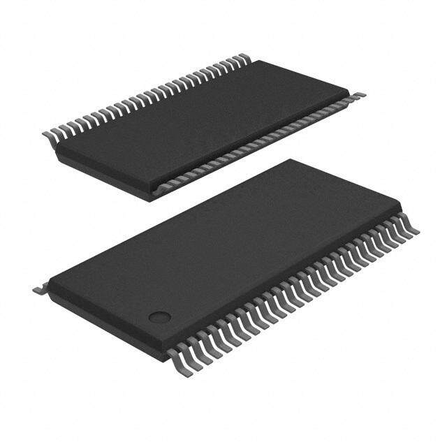
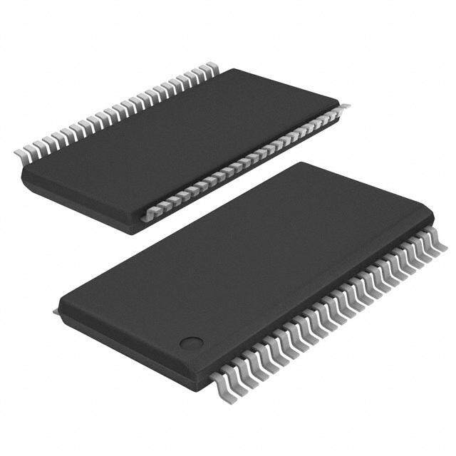
| 描述 | IC BUS TRANSCEIVER DUAL 20SOIC总线收发器 Octal Bus w/OC Out |
| 产品分类 | |
| 品牌 | Texas Instruments |
| 产品手册 | http://www.ti.com/litv/sdas300 |
| 产品图片 |
|
| rohs | 符合RoHS无铅 / 符合限制有害物质指令(RoHS)规范要求 |
| 产品系列 | 逻辑集成电路,总线收发器,Texas Instruments SN74ALS641A-1DW74ALS |
| 数据手册 | |
| 产品型号 | SN74ALS641A-1DW |
| 产品目录页面 | |
| 产品种类 | Logic - Buffers, Drivers, and Transceivers |
| 传播延迟时间 | 25 ns |
| 低电平输出电流 | 48 mA |
| 供应商器件封装 | 20-SOIC |
| 元件数 | 1 |
| 其它名称 | 296-9770-5 |
| 功能 | Octal bus transceivers are designed for asynchronous two-way communication |
| 包装 | 管件 |
| 单位重量 | 500.700 mg |
| 商标 | Texas Instruments |
| 安装类型 | 表面贴装 |
| 安装风格 | SMD/SMT |
| 封装 | Tube |
| 封装/外壳 | 20-SOIC(0.295",7.50mm 宽) |
| 封装/箱体 | SOIC-20 |
| 工作温度 | 0°C ~ 70°C |
| 工厂包装数量 | 25 |
| 最大工作温度 | + 70 C |
| 最小工作温度 | 0 C |
| 极性 | Non-Inverting |
| 标准包装 | 25 |
| 每元件位数 | 8 |
| 每芯片的通道数量 | 8 |
| 电压-电源 | 4.5 V ~ 5.5 V |
| 电流-输出高,低 | -,24mA |
| 电源电压-最大 | 5.25 V |
| 电源电压-最小 | 4.75 V |
| 电路数量 | 8 |
| 系列 | SN74ALS641A-1 |
| 输入电平 | TTL |
| 输出电平 | TTL |
| 输出类型 | Open Collector |
| 逻辑类型 | 收发器,反相 |
| 逻辑系列 | ALS |
| 高电平输出电流 | - 0.1 mA |


PDF Datasheet 数据手册内容提取
(cid:1)(cid:2)(cid:3)(cid:4)(cid:5)(cid:6)(cid:1)(cid:7)(cid:4)(cid:8)(cid:5)(cid:9)(cid:10)(cid:1)(cid:2)(cid:3)(cid:4)(cid:5)(cid:6)(cid:1)(cid:7)(cid:4)(cid:11)(cid:5)(cid:9)(cid:10)(cid:1)(cid:2)(cid:3)(cid:4)(cid:5)(cid:1)(cid:7)(cid:4)(cid:8) (cid:12)(cid:13)(cid:14)(cid:5)(cid:6)(cid:10)(cid:15)(cid:16)(cid:1)(cid:10)(cid:14)(cid:17)(cid:5)(cid:2)(cid:1)(cid:13)(cid:18)(cid:19)(cid:20)(cid:18)(cid:17)(cid:1) (cid:21)(cid:19)(cid:14)(cid:22)(cid:10)(cid:12)(cid:23)(cid:18)(cid:2)(cid:24)(cid:13)(cid:12)(cid:6)(cid:6)(cid:18)(cid:13)(cid:14)(cid:12)(cid:17)(cid:10)(cid:12)(cid:16)(cid:14)(cid:23)(cid:16)(cid:14)(cid:1) SDAS300 − MARCH 1995 • Bidirectional Bus Transceivers in DW OR N PACKAGE High-Density 20-Pin Packages (TOP VIEW) • Choice of True or Inverting Logic • DIR 1 20 VCC Package Options Include Plastic A1 2 19 OE Small-Outline (DW) Packages and A2 3 18 B1 Standard Plastic (N) 300-mil DIPs A3 4 17 B2 A4 5 16 B3 DEVICE LOGIC A5 6 15 B4 SN74ALS641A, SN74AS641 True A6 7 14 B5 SN74ALS642A Inverting A7 8 13 B6 A8 9 12 B7 description GND 10 11 B8 These octal bus transceivers are designed for asynchronous two-way communication between data buses. These devices transmit data from the A bus to the B bus or from the B bus to the A bus, depending upon the level at the direction-control (DIR) input. The output-enable (OE) input disables the device so that the buses are effectively isolated. The -1 versions of the SN74ALS641A and SN74ALS642A are identical to the standard versions, except that the recommended maximum I is increased to 48 mA in the -1 versions. OL The SN74ALS641A, SN74ALS642A, and SN74AS641 are characterized for operation from 0°C to 70°C. FUNCTION TABLE INPUTS OPERATION SN74ALS641A OE DIR SN74ALS642A SN74AS641 L L B data to A bus B data to A bus L H A data to B bus A data to B bus H X Isolation Isolation (cid:23)(cid:17)(cid:12)(cid:25)(cid:16)(cid:13)(cid:14)(cid:19)(cid:12)(cid:2) (cid:25)(cid:5)(cid:14)(cid:5) (cid:26)(cid:27)(cid:28)(cid:29)(cid:30)(cid:31)!"(cid:26)(cid:29)(cid:27) (cid:26)# $%(cid:30)(cid:30)&(cid:27)" !# (cid:29)(cid:28) ’%()(cid:26)$!"(cid:26)(cid:29)(cid:27) *!"&+ Copyright 1995, Texas Instruments Incorporated (cid:23)(cid:30)(cid:29)*%$"# $(cid:29)(cid:27)(cid:28)(cid:29)(cid:30)(cid:31) "(cid:29) #’&$(cid:26)(cid:28)(cid:26)$!"(cid:26)(cid:29)(cid:27)# ’&(cid:30) ",& "&(cid:30)(cid:31)# (cid:29)(cid:28) (cid:14)&-!# (cid:19)(cid:27)#"(cid:30)%(cid:31)&(cid:27)"# #"!(cid:27)*!(cid:30)* .!(cid:30)(cid:30)!(cid:27)"/+ (cid:23)(cid:30)(cid:29)*%$"(cid:26)(cid:29)(cid:27) ’(cid:30)(cid:29)$&##(cid:26)(cid:27)0 *(cid:29)&# (cid:27)(cid:29)" (cid:27)&$&##!(cid:30)(cid:26))/ (cid:26)(cid:27)$)%*& "&#"(cid:26)(cid:27)0 (cid:29)(cid:28) !)) ’!(cid:30)!(cid:31)&"&(cid:30)#+ POST OFFICE BOX 655303 • DALLAS, TEXAS 75265 1 • POST OFFICE BOX 1443 HOUSTON, TEXAS 77251−1443
(cid:1)(cid:2)(cid:3)(cid:4)(cid:5)(cid:6)(cid:1)(cid:7)(cid:4)(cid:8)(cid:5)(cid:9)(cid:10)(cid:1)(cid:2)(cid:3)(cid:4)(cid:5)(cid:6)(cid:1)(cid:7)(cid:4)(cid:11)(cid:5)(cid:9)(cid:10)(cid:1)(cid:2)(cid:3)(cid:4)(cid:5)(cid:1)(cid:7)(cid:4)(cid:8) (cid:12)(cid:13)(cid:14)(cid:5)(cid:6)(cid:10)(cid:15)(cid:16)(cid:1)(cid:10)(cid:14)(cid:17)(cid:5)(cid:2)(cid:1)(cid:13)(cid:18)(cid:19)(cid:20)(cid:18)(cid:17)(cid:1) (cid:21)(cid:19)(cid:14)(cid:22)(cid:10)(cid:12)(cid:23)(cid:18)(cid:2)(cid:24)(cid:13)(cid:12)(cid:6)(cid:6)(cid:18)(cid:13)(cid:14)(cid:12)(cid:17)(cid:10)(cid:12)(cid:16)(cid:14)(cid:23)(cid:16)(cid:14)(cid:1) SDAS300 − MARCH 1995 logic symbols† SN74ALS641A, SN74AS641 SN74ALS642A 19 19 OE G3 OE G3 1 1 DIR 3 EN1 [BA] DIR 3 EN1 [BA] 3 EN2 [AB] 3 EN2 [AB] 2 18 2 18 A1 1 B1 A1 1 B1 2 2 3 17 3 17 A2 B2 A2 B2 4 16 4 16 A3 B3 A3 B3 5 15 5 15 A4 B4 A4 B4 6 14 6 14 A5 B5 A5 B5 7 13 7 13 A6 B6 A6 B6 8 12 8 12 A7 B7 A7 B7 9 11 9 11 A8 B8 A8 B8 †These symbols are in accordance with ANSI/IEEE Std 91-1984 and IEC Publication 617-12. 2 POST OFFICE BOX 65•5303 • DALLAS, TEXAS 75265 POST OFFICE BOX 1443 HOUSTON, TEXAS 77251−1443
(cid:1)(cid:2)(cid:3)(cid:4)(cid:5)(cid:6)(cid:1)(cid:7)(cid:4)(cid:8)(cid:5)(cid:9)(cid:10)(cid:1)(cid:2)(cid:3)(cid:4)(cid:5)(cid:6)(cid:1)(cid:7)(cid:4)(cid:11)(cid:5)(cid:9)(cid:10)(cid:1)(cid:2)(cid:3)(cid:4)(cid:5)(cid:1)(cid:7)(cid:4)(cid:8) (cid:12)(cid:13)(cid:14)(cid:5)(cid:6)(cid:10)(cid:15)(cid:16)(cid:1)(cid:10)(cid:14)(cid:17)(cid:5)(cid:2)(cid:1)(cid:13)(cid:18)(cid:19)(cid:20)(cid:18)(cid:17)(cid:1) (cid:21)(cid:19)(cid:14)(cid:22)(cid:10)(cid:12)(cid:23)(cid:18)(cid:2)(cid:24)(cid:13)(cid:12)(cid:6)(cid:6)(cid:18)(cid:13)(cid:14)(cid:12)(cid:17)(cid:10)(cid:12)(cid:16)(cid:14)(cid:23)(cid:16)(cid:14)(cid:1) SDAS300 − MARCH 1995 logic diagrams (positive logic) SN74ALS641A, SN74AS641 SN74ALS642A 19 19 OE OE 1 1 DIR DIR 18 18 2 B1 2 B1 A1 A1 To Seven Other Transceivers To Seven Other Transceivers absolute maximum ratings over operating free-air temperature range (unless otherwise noted)† Supply voltage, V . . . . . . . . . . . . . . . . . . . . . . . . . . . . . . . . . . . . . . . . . . . . . . . . . . . . . . . . . . . . . . . . . . . . . . . . 7 V CC Input voltage, V: All inputs and I/O ports . . . . . . . . . . . . . . . . . . . . . . . . . . . . . . . . . . . . . . . . . . . . . . . . . . . . . . 7 V I Operating free-air temperature range, T : SN74ALS641A, SN74ALS642A . . . . . . . . . . . . . . . . . 0°C to 70°C A Storage temperature range . . . . . . . . . . . . . . . . . . . . . . . . . . . . . . . . . . . . . . . . . . . . . . . . . . . . . . . . −65°C to 150°C †Stresses beyond those listed under “absolute maximum ratings” may cause permanent damage to the device. These are stress ratings only, and functional operation of the device at these or any other conditions beyond those indicated under “recommended operating conditions” is not implied. Exposure to absolute-maximum-rated conditions for extended periods may affect device reliability. recommended operating conditions SN74ALS641A SN74ALS642A UUNNIITT MIN NOM MAX VCC Supply voltage 4.5 5 5.5 V VIH High-level input voltage 2 V VIL Low-level input voltage 0.8 V VOH High-level output voltage 5.5 V 24 IIOOLL LLooww--lleevveell oouuttppuutt ccuurrrreenntt 48‡ mmAA TA Operating free-air temperature 0 70 °C ‡Applies only to the -1 version and only if VCC is between 4.75 V and 5.25 V POST OFFICE BOX 65•5303 • DALLAS, TEXAS 75265 3 POST OFFICE BOX 1443 HOUSTON, TEXAS 77251−1443
(cid:1)(cid:2)(cid:3)(cid:4)(cid:5)(cid:6)(cid:1)(cid:7)(cid:4)(cid:8)(cid:5)(cid:9)(cid:10)(cid:1)(cid:2)(cid:3)(cid:4)(cid:5)(cid:6)(cid:1)(cid:7)(cid:4)(cid:11)(cid:5)(cid:9)(cid:10)(cid:1)(cid:2)(cid:3)(cid:4)(cid:5)(cid:1)(cid:7)(cid:4)(cid:8) (cid:12)(cid:13)(cid:14)(cid:5)(cid:6)(cid:10)(cid:15)(cid:16)(cid:1)(cid:10)(cid:14)(cid:17)(cid:5)(cid:2)(cid:1)(cid:13)(cid:18)(cid:19)(cid:20)(cid:18)(cid:17)(cid:1) (cid:21)(cid:19)(cid:14)(cid:22)(cid:10)(cid:12)(cid:23)(cid:18)(cid:2)(cid:24)(cid:13)(cid:12)(cid:6)(cid:6)(cid:18)(cid:13)(cid:14)(cid:12)(cid:17)(cid:10)(cid:12)(cid:16)(cid:14)(cid:23)(cid:16)(cid:14)(cid:1) SDAS300 − MARCH 1995 electrical characteristics over recommended operating free-air temperature range (unless otherwise noted) SN74ALS641A PPAARRAAMMEETTEERR TTEESSTT CCOONNDDIITTIIOONNSS SN74ALS642A UUNNIITT MIN TYP† MAX VIK VCC = 4.5 V, II = −18 mA −1.5 V IOH VCC = 4.5 V, VOH = 5.5 V 0.1 mA IOL = 12 mA 0.25 0.4 VVOOLL VVCCCC == 44..55 VV IOL = 24 mA 0.35 0.5 VV IOL = 48 mA‡ 0.35 0.5 II Control inputs VCC = 5.5 V, VI = 7 V 0.1 mA Control inputs 20 IIIIHH A or B ports§ VVCCCC == 55..55 VV,, VVII == 22..77 VV 20 µAA Control inputs −0.1 IIIILL A or B ports§ VVCCCC == 55..55 VV,, VVII == 00..44 VV −0.1 mmAA Outputs high 25 37 SSNN7744AALLSS664411AA VVCCCC == 55..55 VV Outputs low 33 47 IICCCC mmAA Outputs high 8 15 SSNN7744AALLSS664422AA VVCCCC == 55..55 VV Outputs low 18 28 †All typical values are at VCC = 5 V, TA = 25°C. ‡Applies only to the -1 version and only if VCC is between 4.75 V and 5.25 V §For I/O ports, the parameters IIH and IIL include the off-state output current. switching characteristics (see Figure 1) VCC = 4.5 V to 5.5 V, CL = 50 pF, FROM TO RL = 680 Ω, PPAARRAAMMEETTEERR ((IINNPPUUTT)) ((OOUUTTPPUUTT)) TA = MIN to MAX¶ UUNNIITT SN74ALS641A SN74ALS642A MIN MAX MIN MAX tPLH 5 25 10 30 AA oorr BB BB oorr AA nnss tPHL 3 18 5 22 tPLH 8 30 10 30 OOEE AA oorr BB nnss tPHL 8 30 15 38 tPLH 8 32 10 30 DDIIRR AA oorr BB nnss tPHL 8 32 15 38 ¶For conditions shown as MIN or MAX, use the appropriate value specified under recommended operating conditions. 4 POST OFFICE BOX 65•5303 • DALLAS, TEXAS 75265 POST OFFICE BOX 1443 HOUSTON, TEXAS 77251−1443
(cid:1)(cid:2)(cid:3)(cid:4)(cid:5)(cid:6)(cid:1)(cid:7)(cid:4)(cid:8)(cid:5)(cid:9)(cid:10)(cid:1)(cid:2)(cid:3)(cid:4)(cid:5)(cid:6)(cid:1)(cid:7)(cid:4)(cid:11)(cid:5)(cid:9)(cid:10)(cid:1)(cid:2)(cid:3)(cid:4)(cid:5)(cid:1)(cid:7)(cid:4)(cid:8) (cid:12)(cid:13)(cid:14)(cid:5)(cid:6)(cid:10)(cid:15)(cid:16)(cid:1)(cid:10)(cid:14)(cid:17)(cid:5)(cid:2)(cid:1)(cid:13)(cid:18)(cid:19)(cid:20)(cid:18)(cid:17)(cid:1) (cid:21)(cid:19)(cid:14)(cid:22)(cid:10)(cid:12)(cid:23)(cid:18)(cid:2)(cid:24)(cid:13)(cid:12)(cid:6)(cid:6)(cid:18)(cid:13)(cid:14)(cid:12)(cid:17)(cid:10)(cid:12)(cid:16)(cid:14)(cid:23)(cid:16)(cid:14)(cid:1) SDAS300 − MARCH 1995 absolute maximum ratings over operating free-air temperature range (unless otherwise noted)† Supply voltage, V . . . . . . . . . . . . . . . . . . . . . . . . . . . . . . . . . . . . . . . . . . . . . . . . . . . . . . . . . . . . . . . . . . . . . . . . 7 V CC Input voltage, V: All inputs and I/O ports . . . . . . . . . . . . . . . . . . . . . . . . . . . . . . . . . . . . . . . . . . . . . . . . . . . . . . 7 V I Operating free-air temperature range, T : SN74AS641 . . . . . . . . . . . . . . . . . . . . . . . . . . . . . . . . . . 0°C to 70°C A Storage temperature range . . . . . . . . . . . . . . . . . . . . . . . . . . . . . . . . . . . . . . . . . . . . . . . . . . . . . . . . −65°C to 150°C †Stresses beyond those listed under “absolute maximum ratings” may cause permanent damage to the device. These are stress ratings only, and functional operation of the device at these or any other conditions beyond those indicated under “recommended operating conditions” is not implied. Exposure to absolute-maximum-rated conditions for extended periods may affect device reliability. recommended operating conditions SN74AS641 UUNNIITT MIN NOM MAX VCC Supply voltage 4.5 5 5.5 V VIH High-level input voltage 2 V VIL Low-level input voltage 0.8 V VOH High-level output voltage 5.5 V IOL Low-level output current 64 mA TA Operating free-air temperature 0 70 °C electrical characteristics over recommended operating free-air temperature range (unless otherwise noted) SN74AS641 PPAARRAAMMEETTEERR TTEESSTT CCOONNDDIITTIIOONNSS UUNNIITT MIN TYP‡ MAX VIK VCC = 4.5 V, II = −18 mA −1.2 V IOH VCC = 4.5 V, VOH = 5.5 V 0.1 mA VOL VCC = 4.5 V, IOL = 64 mA 0.35 0.55 V Control inputs VI = 7 V 0.1 IIII VVCCCC == 55..55 VV mmAA A or B ports VI = 5.5 V 0.1 Control inputs 20 IIIIHH A or B ports§ VVCCCC == 55..55 VV,, VVII == 22..77 VV 70 µAA Control inputs −0.5 IIIILL A or B ports§ VVCCCC == 55..55 VV,, VVII == 00..44 VV −0.75 mmAA Outputs high 50 82 IICCCC VVCCCC == 55..55 VV mmAA Outputs low 84 136 ‡All typical values are at VCC = 5 V, TA = 25°C. §For I/O ports, the parameters IIH and IIL include the off-state output current. POST OFFICE BOX 65•5303 • DALLAS, TEXAS 75265 5 POST OFFICE BOX 1443 HOUSTON, TEXAS 77251−1443
(cid:1)(cid:2)(cid:3)(cid:4)(cid:5)(cid:6)(cid:1)(cid:7)(cid:4)(cid:8)(cid:5)(cid:9)(cid:10)(cid:1)(cid:2)(cid:3)(cid:4)(cid:5)(cid:6)(cid:1)(cid:7)(cid:4)(cid:11)(cid:5)(cid:9)(cid:10)(cid:1)(cid:2)(cid:3)(cid:4)(cid:5)(cid:1)(cid:7)(cid:4)(cid:8) (cid:12)(cid:13)(cid:14)(cid:5)(cid:6)(cid:10)(cid:15)(cid:16)(cid:1)(cid:10)(cid:14)(cid:17)(cid:5)(cid:2)(cid:1)(cid:13)(cid:18)(cid:19)(cid:20)(cid:18)(cid:17)(cid:1) (cid:21)(cid:19)(cid:14)(cid:22)(cid:10)(cid:12)(cid:23)(cid:18)(cid:2)(cid:24)(cid:13)(cid:12)(cid:6)(cid:6)(cid:18)(cid:13)(cid:14)(cid:12)(cid:17)(cid:10)(cid:12)(cid:16)(cid:14)(cid:23)(cid:16)(cid:14)(cid:1) SDAS300 − MARCH 1995 switching characteristics (see Figure 1) VCC = 4.5 V to 5.5 V, CL = 50 pF, FROM TO RL = 680 Ω, PPAARRAAMMEETTEERR ((IINNPPUUTT)) ((OOUUTTPPUUTT)) TA = MIN to MAX† UUNNIITT SN74AS641 MIN MAX tPLH 5 21 AA oorr BB BB oorr AA nnss tPHL 1 7.5 tPLH 5 21 OOEE AA oorr BB nnss tPHL 1 9 tPLH 5 22 DDIIRR AA oorr BB nnss tPHL 1 10 †For conditions shown as MIN or MAX, use the appropriate value specified under recommended operating conditions. 6 POST OFFICE BOX 65•5303 • DALLAS, TEXAS 75265 POST OFFICE BOX 1443 HOUSTON, TEXAS 77251−1443
(cid:1)(cid:2)(cid:3)(cid:4)(cid:5)(cid:6)(cid:1)(cid:7)(cid:4)(cid:8)(cid:5)(cid:9)(cid:10)(cid:1)(cid:2)(cid:3)(cid:4)(cid:5)(cid:6)(cid:1)(cid:7)(cid:4)(cid:11)(cid:5)(cid:9)(cid:10)(cid:1)(cid:2)(cid:3)(cid:4)(cid:5)(cid:1)(cid:7)(cid:4)(cid:8) (cid:12)(cid:13)(cid:14)(cid:5)(cid:6)(cid:10)(cid:15)(cid:16)(cid:1)(cid:10)(cid:14)(cid:17)(cid:5)(cid:2)(cid:1)(cid:13)(cid:18)(cid:19)(cid:20)(cid:18)(cid:17)(cid:1) (cid:21)(cid:19)(cid:14)(cid:22)(cid:10)(cid:12)(cid:23)(cid:18)(cid:2)(cid:24)(cid:13)(cid:12)(cid:6)(cid:6)(cid:18)(cid:13)(cid:14)(cid:12)(cid:17)(cid:10)(cid:12)(cid:16)(cid:14)(cid:23)(cid:16)(cid:14)(cid:1) SDAS300 − MARCH 1995 PARAMETER MEASUREMENT INFORMATION SERIES 54ALS/74ALS AND 54AS/74AS DEVICES 7 V VCC RL = R1 = R2 S1 RL R1 From Output Test From Output Test From Output Test Under Test Point Under Test Point Under Test Point (see Note CAL) RL CL (see Note CAL) R2 (see Note A) LOAD CIRCUIT FOR BI-STATE LOAD CIRCUIT LOAD CIRCUIT TOTEM-POLE OUTPUTS FOR OPEN-COLLECTOR OUTPUTS FOR 3-STATE OUTPUTS 3.5 V 3.5 V Timing High-Level Input 1.3 V Pulse 1.3 V 1.3 V 0.3 V 0.3 V tsu th tw 3.5 V 3.5 V Data Low-Level Input 1.3 V 1.3 V Pulse 1.3 V 1.3 V 0.3 V 0.3 V VOLTAGE WAVEFORMS VOLTAGE WAVEFORMS SETUP AND HOLD TIMES PULSE DURATIONS 3.5 V Output Control 1.3 V 1.3 V (low-level enabling) 0.3 V 3.5 V tPZL Input 1.3 V 1.3 V tPLZ 0.3 V (cid:1)3.5 V Waveform 1 tPLH tPHL S1 Closed 1.3 V In-Phase VOH (see Note B) VOL Output 1.3 V 1.3 V tPHZ 0.3 V VOL tPZH tPLH VOH tPHL Waveform 2 Out-of-Phase VOH S1 Open 1.3 V 0.3 V Output 1.3 V 1.3 V (see Note B) (cid:1)0 V (see Note C) VOL VOLTAGE WAVEFORMS VOLTAGE WAVEFORMS ENABLE AND DISABLE TIMES, 3-STATE OUTPUTS PROPAGATION DELAY TIMES NOTES: A. CL includes probe and jig capacitance. B. Waveform 1 is for an output with internal conditions such that the output is low except when disabled by the output control. Waveform 2 is for an output with internal conditions such that the output is high except when disabled by the output control. C. When measuring propagation delay items of 3-state outputs, switch S1 is open. D. All input pulses have the following characteristics: PRR ≤ 1 MHz, tr = tf = 2 ns, duty cycle = 50%. E. The outputs are measured one at a time with one transition per measurement. Figure 1. Load Circuits and Voltage Waveforms POST OFFICE BOX 65•5303 • DALLAS, TEXAS 75265 7 POST OFFICE BOX 1443 HOUSTON, TEXAS 77251−1443
PACKAGE OPTION ADDENDUM www.ti.com 6-Feb-2020 PACKAGING INFORMATION Orderable Device Status Package Type Package Pins Package Eco Plan Lead/Ball Finish MSL Peak Temp Op Temp (°C) Device Marking Samples (1) Drawing Qty (2) (6) (3) (4/5) SN74ALS641A-1DW ACTIVE SOIC DW 20 25 Green (RoHS NIPDAU Level-1-260C-UNLIM 0 to 70 ALS641A-1 & no Sb/Br) SN74ALS641A-1DWR ACTIVE SOIC DW 20 2000 Green (RoHS NIPDAU Level-1-260C-UNLIM 0 to 70 ALS641A-1 & no Sb/Br) SN74ALS641A-1N ACTIVE PDIP N 20 20 Pb-Free NIPDAU N / A for Pkg Type 0 to 70 SN74ALS641A-1N (RoHS) SN74ALS641A-1NSR ACTIVE SO NS 20 2000 Green (RoHS NIPDAU Level-1-260C-UNLIM 0 to 70 ALS641A-1 & no Sb/Br) SN74ALS641ADW ACTIVE SOIC DW 20 25 Green (RoHS NIPDAU Level-1-260C-UNLIM 0 to 70 ALS641A & no Sb/Br) SN74ALS641ADWR ACTIVE SOIC DW 20 2000 Green (RoHS NIPDAU Level-1-260C-UNLIM 0 to 70 ALS641A & no Sb/Br) SN74ALS641AN ACTIVE PDIP N 20 20 Pb-Free NIPDAU N / A for Pkg Type 0 to 70 SN74ALS641AN (RoHS) SN74ALS641ANSR ACTIVE SO NS 20 2000 Green (RoHS NIPDAU Level-1-260C-UNLIM 0 to 70 ALS641A & no Sb/Br) SN74ALS642A-1DW ACTIVE SOIC DW 20 25 Green (RoHS NIPDAU Level-1-260C-UNLIM 0 to 70 ALS642A-1 & no Sb/Br) SN74ALS642A-1N ACTIVE PDIP N 20 20 Pb-Free NIPDAU N / A for Pkg Type 0 to 70 SN74ALS642A-1N (RoHS) SN74ALS642A-1NSR ACTIVE SO NS 20 2000 Green (RoHS NIPDAU Level-1-260C-UNLIM 0 to 70 ALS642A-1 & no Sb/Br) SN74AS641DW ACTIVE SOIC DW 20 25 Green (RoHS NIPDAU Level-1-260C-UNLIM 0 to 70 AS641 & no Sb/Br) SN74AS641N ACTIVE PDIP N 20 20 Pb-Free NIPDAU N / A for Pkg Type 0 to 70 SN74AS641N (RoHS) (1) The marketing status values are defined as follows: ACTIVE: Product device recommended for new designs. LIFEBUY: TI has announced that the device will be discontinued, and a lifetime-buy period is in effect. NRND: Not recommended for new designs. Device is in production to support existing customers, but TI does not recommend using this part in a new design. PREVIEW: Device has been announced but is not in production. Samples may or may not be available. OBSOLETE: TI has discontinued the production of the device. Addendum-Page 1
PACKAGE OPTION ADDENDUM www.ti.com 6-Feb-2020 (2) RoHS: TI defines "RoHS" to mean semiconductor products that are compliant with the current EU RoHS requirements for all 10 RoHS substances, including the requirement that RoHS substance do not exceed 0.1% by weight in homogeneous materials. Where designed to be soldered at high temperatures, "RoHS" products are suitable for use in specified lead-free processes. TI may reference these types of products as "Pb-Free". RoHS Exempt: TI defines "RoHS Exempt" to mean products that contain lead but are compliant with EU RoHS pursuant to a specific EU RoHS exemption. Green: TI defines "Green" to mean the content of Chlorine (Cl) and Bromine (Br) based flame retardants meet JS709B low halogen requirements of <=1000ppm threshold. Antimony trioxide based flame retardants must also meet the <=1000ppm threshold requirement. (3) MSL, Peak Temp. - The Moisture Sensitivity Level rating according to the JEDEC industry standard classifications, and peak solder temperature. (4) There may be additional marking, which relates to the logo, the lot trace code information, or the environmental category on the device. (5) Multiple Device Markings will be inside parentheses. Only one Device Marking contained in parentheses and separated by a "~" will appear on a device. If a line is indented then it is a continuation of the previous line and the two combined represent the entire Device Marking for that device. (6) Lead/Ball Finish - Orderable Devices may have multiple material finish options. Finish options are separated by a vertical ruled line. Lead/Ball Finish values may wrap to two lines if the finish value exceeds the maximum column width. Important Information and Disclaimer:The information provided on this page represents TI's knowledge and belief as of the date that it is provided. TI bases its knowledge and belief on information provided by third parties, and makes no representation or warranty as to the accuracy of such information. Efforts are underway to better integrate information from third parties. TI has taken and continues to take reasonable steps to provide representative and accurate information but may not have conducted destructive testing or chemical analysis on incoming materials and chemicals. TI and TI suppliers consider certain information to be proprietary, and thus CAS numbers and other limited information may not be available for release. In no event shall TI's liability arising out of such information exceed the total purchase price of the TI part(s) at issue in this document sold by TI to Customer on an annual basis. Addendum-Page 2
PACKAGE MATERIALS INFORMATION www.ti.com 6-May-2017 TAPE AND REEL INFORMATION *Alldimensionsarenominal Device Package Package Pins SPQ Reel Reel A0 B0 K0 P1 W Pin1 Type Drawing Diameter Width (mm) (mm) (mm) (mm) (mm) Quadrant (mm) W1(mm) SN74ALS641A-1DWR SOIC DW 20 2000 330.0 24.4 10.8 13.3 2.7 12.0 24.0 Q1 SN74ALS641A-1NSR SO NS 20 2000 330.0 24.4 8.4 13.0 2.5 12.0 24.0 Q1 SN74ALS641ADWR SOIC DW 20 2000 330.0 24.4 10.8 13.3 2.7 12.0 24.0 Q1 SN74ALS641ANSR SO NS 20 2000 330.0 24.4 8.4 13.0 2.5 12.0 24.0 Q1 SN74ALS642A-1NSR SO NS 20 2000 330.0 24.4 8.4 13.0 2.5 12.0 24.0 Q1 PackMaterials-Page1
PACKAGE MATERIALS INFORMATION www.ti.com 6-May-2017 *Alldimensionsarenominal Device PackageType PackageDrawing Pins SPQ Length(mm) Width(mm) Height(mm) SN74ALS641A-1DWR SOIC DW 20 2000 367.0 367.0 45.0 SN74ALS641A-1NSR SO NS 20 2000 367.0 367.0 45.0 SN74ALS641ADWR SOIC DW 20 2000 367.0 367.0 45.0 SN74ALS641ANSR SO NS 20 2000 367.0 367.0 45.0 SN74ALS642A-1NSR SO NS 20 2000 367.0 367.0 45.0 PackMaterials-Page2
None
None
PACKAGE OUTLINE DW0020A SOIC - 2.65 mm max height SCALE 1.200 SOIC C 10.63 SEATING PLANE TYP 9.97 A PIN 1 ID 0.1 C AREA 18X 1.27 20 1 13.0 2X 12.6 11.43 NOTE 3 10 11 0.51 20X 7.6 0.31 2.65 MAX B 7.4 0.25 C A B NOTE 4 0.33 TYP 0.10 0.25 SEE DETAIL A GAGE PLANE 0.3 1.27 0 - 8 0.1 0.40 DETAIL A TYPICAL 4220724/A 05/2016 NOTES: 1. All linear dimensions are in millimeters. Dimensions in parenthesis are for reference only. Dimensioning and tolerancing per ASME Y14.5M. 2. This drawing is subject to change without notice. 3. This dimension does not include mold flash, protrusions, or gate burrs. Mold flash, protrusions, or gate burrs shall not exceed 0.15 mm per side. 4. This dimension does not include interlead flash. Interlead flash shall not exceed 0.43 mm per side. 5. Reference JEDEC registration MS-013. www.ti.com
EXAMPLE BOARD LAYOUT DW0020A SOIC - 2.65 mm max height SOIC 20X (2) SYMM 1 20 20X (0.6) 18X (1.27) SYMM (R0.05) TYP 10 11 (9.3) LAND PATTERN EXAMPLE SCALE:6X SOOPLEDNEINRG MASK METAL MSOELTDAEL RU NMDAESRK SOOPLEDNEINRG MASK 0.07 MAX 0.07 MIN ALL AROUND ALL AROUND NON SOLDER MASK SOLDER MASK DEFINED DEFINED SOLDER MASK DETAILS 4220724/A 05/2016 NOTES: (continued) 6. Publication IPC-7351 may have alternate designs. 7. Solder mask tolerances between and around signal pads can vary based on board fabrication site. www.ti.com
EXAMPLE STENCIL DESIGN DW0020A SOIC - 2.65 mm max height SOIC 20X (2) SYMM 1 20 20X (0.6) 18X (1.27) SYMM 10 11 (9.3) SOLDER PASTE EXAMPLE BASED ON 0.125 mm THICK STENCIL SCALE:6X 4220724/A 05/2016 NOTES: (continued) 8. Laser cutting apertures with trapezoidal walls and rounded corners may offer better paste release. IPC-7525 may have alternate design recommendations. 9. Board assembly site may have different recommendations for stencil design. www.ti.com
IMPORTANTNOTICEANDDISCLAIMER TI PROVIDES TECHNICAL AND RELIABILITY DATA (INCLUDING DATASHEETS), DESIGN RESOURCES (INCLUDING REFERENCE DESIGNS), APPLICATION OR OTHER DESIGN ADVICE, WEB TOOLS, SAFETY INFORMATION, AND OTHER RESOURCES “AS IS” AND WITH ALL FAULTS, AND DISCLAIMS ALL WARRANTIES, EXPRESS AND IMPLIED, INCLUDING WITHOUT LIMITATION ANY IMPLIED WARRANTIES OF MERCHANTABILITY, FITNESS FOR A PARTICULAR PURPOSE OR NON-INFRINGEMENT OF THIRD PARTY INTELLECTUAL PROPERTY RIGHTS. These resources are intended for skilled developers designing with TI products. You are solely responsible for (1) selecting the appropriate TI products for your application, (2) designing, validating and testing your application, and (3) ensuring your application meets applicable standards, and any other safety, security, or other requirements. These resources are subject to change without notice. TI grants you permission to use these resources only for development of an application that uses the TI products described in the resource. Other reproduction and display of these resources is prohibited. No license is granted to any other TI intellectual property right or to any third party intellectual property right. TI disclaims responsibility for, and you will fully indemnify TI and its representatives against, any claims, damages, costs, losses, and liabilities arising out of your use of these resources. TI’s products are provided subject to TI’s Terms of Sale (www.ti.com/legal/termsofsale.html) or other applicable terms available either on ti.com or provided in conjunction with such TI products. TI’s provision of these resources does not expand or otherwise alter TI’s applicable warranties or warranty disclaimers for TI products. Mailing Address: Texas Instruments, Post Office Box 655303, Dallas, Texas 75265 Copyright © 2020, Texas Instruments Incorporated