ICGOO在线商城 > 集成电路(IC) > 逻辑 - 缓冲器,驱动器,接收器,收发器 > SN74AHCT541PW
 Datasheet下载
- 型号: SN74AHCT541PW
- 制造商: Texas Instruments
- 库位|库存: xxxx|xxxx
- 要求:
| 数量阶梯 | 香港交货 | 国内含税 |
| +xxxx | $xxxx | ¥xxxx |
查看当月历史价格
查看今年历史价格
SN74AHCT541PW产品简介:
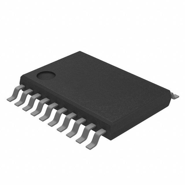
ICGOO电子元器件商城为您提供SN74AHCT541PW由Texas Instruments设计生产,在icgoo商城现货销售,并且可以通过原厂、代理商等渠道进行代购。 SN74AHCT541PW价格参考¥3.52-¥3.52。Texas InstrumentsSN74AHCT541PW封装/规格:逻辑 - 缓冲器,驱动器,接收器,收发器, Buffer, Non-Inverting 1 Element 8 Bit per Element 3-State Output 20-TSSOP。您可以下载SN74AHCT541PW参考资料、Datasheet数据手册功能说明书,资料中有SN74AHCT541PW 详细功能的应用电路图电压和使用方法及教程。
SN74AHCT541PW 是由 Texas Instruments 生产的一款逻辑缓冲器、驱动器、接收器和收发器。它广泛应用于需要在不同逻辑电平之间进行信号转换或扩展的场景,特别是在数字电路设计中。

 主要应用场景:

1. 总线扩展与隔离:
   - 该器件常用于扩展数据总线,例如将8位数据总线扩展为多个设备共享的总线系统。它可以确保信号完整性,避免信号冲突。
   - 在多主控系统中,SN74AHCT541PW 可以作为隔离器,防止不同模块之间的信号干扰。

2. 电平转换:
   - SN74AHCT541PW 支持不同的电源电压(Vcc = 2V 至 6V),因此可以用于在不同电压电平的系统之间进行信号转换。例如,在3.3V和5V系统之间传输数据时,它可以确保信号兼容性。

3. 驱动能力增强:
   - 当负载较大或信号需要长距离传输时,普通的逻辑门可能无法提供足够的驱动能力。SN74AHCT541PW 可以增强信号的驱动能力,确保信号在传输过程中不失真。

4. 接口扩展:
   - 在嵌入式系统中,SN74AHCT541PW 可以用于扩展I/O接口。例如,当微控制器的GPIO引脚不足时,可以通过该器件扩展更多的输入输出通道。

5. 通信接口:
   - 在某些通信协议中,如SPI、I2C等,SN74AHCT541PW 可以用作双向收发器,确保数据在发送和接收之间的正确传输。特别是在多设备共用同一总线的情况下,它可以有效管理信号的流向。

6. 工业控制与自动化:
   - 在工业控制系统中,SN74AHCT541PW 可以用于连接不同的传感器、执行器和其他外围设备,确保信号的可靠传输和处理。

总之,SN74AHCT541PW 是一款多功能的逻辑缓冲器和收发器,适用于各种需要信号扩展、电平转换和驱动能力增强的场合。其高可靠性和广泛的适用性使其成为许多数字电路设计中的首选器件。
| 参数 | 数值 |
| 产品目录 | 集成电路 (IC)半导体 |
| 描述 | IC BUFF/DVR TRI-ST 8BIT 20TSSOP缓冲器和线路驱动器 Octal w/Tri-St Out |
| 产品分类 | |
| 品牌 | Texas Instruments |
| 产品手册 | |
| 产品图片 |
|
| rohs | 符合RoHS无铅 / 符合限制有害物质指令(RoHS)规范要求 |
| 产品系列 | 逻辑集成电路,缓冲器和线路驱动器,Texas Instruments SN74AHCT541PW74AHCT |
| 数据手册 | |
| 产品型号 | SN74AHCT541PW |
| 产品种类 | 缓冲器和线路驱动器 |
| 传播延迟时间 | 8.5 ns at 5 V |
| 低电平输出电流 | 8 mA |
| 供应商器件封装 | 20-TSSOP |
| 元件数 | 1 |
| 其它名称 | 296-26424-5 |
| 包装 | 管件 |
| 单位重量 | 77 mg |
| 商标 | Texas Instruments |
| 安装类型 | 表面贴装 |
| 安装风格 | SMD/SMT |
| 封装 | Tube |
| 封装/外壳 | 20-TSSOP(0.173",4.40mm 宽) |
| 封装/箱体 | TSSOP-20 |
| 工作温度 | -40°C ~ 125°C |
| 工厂包装数量 | 70 |
| 最大工作温度 | + 85 C |
| 最小工作温度 | - 40 C |
| 极性 | Non-Inverting |
| 标准包装 | 70 |
| 每元件位数 | 8 |
| 每芯片的通道数量 | 8 |
| 电压-电源 | 4.5 V ~ 5.5 V |
| 电流-输出高,低 | 8mA,8mA |
| 电源电压-最大 | 5.5 V |
| 电源电压-最小 | 4.5 V |
| 电源电流 | 0.02 mA |
| 系列 | SN74AHCT541 |
| 输入线路数量 | 8 |
| 输出类型 | 3-State |
| 输出线路数量 | 8 |
| 逻辑类型 | 缓冲器/线路驱动器,非反相 |
| 逻辑系列 | AHCT |
| 高电平输出电流 | - 8 mA |


- 商务部:美国ITC正式对集成电路等产品启动337调查
- 曝三星4nm工艺存在良率问题 高通将骁龙8 Gen1或转产台积电
- 太阳诱电将投资9.5亿元在常州建新厂生产MLCC 预计2023年完工
- 英特尔发布欧洲新工厂建设计划 深化IDM 2.0 战略
- 台积电先进制程称霸业界 有大客户加持明年业绩稳了
- 达到5530亿美元!SIA预计今年全球半导体销售额将创下新高
- 英特尔拟将自动驾驶子公司Mobileye上市 估值或超500亿美元
- 三星加码芯片和SET,合并消费电子和移动部门,撤换高东真等 CEO
- 三星电子宣布重大人事变动 还合并消费电子和移动部门
- 海关总署:前11个月进口集成电路产品价值2.52万亿元 增长14.8%


PDF Datasheet 数据手册内容提取
SN54AHCT541 SN74AHCT541 www.ti.com SCLS269P–OCTOBER1995–REVISEDJUNE2013 OCTAL BUFFERS/DRIVERS WITH 3-STATE OUTPUTS CheckforSamples:SN54AHCT541,SN74AHCT541 FEATURES 1 SN54AHCT541 . . . J or W PACKAGE • InputsAreTTL-VoltageCompatible SN74AHCT541...DB,DGV,DW,N,NS,ORPWPACKAGE • Latch-UpPerformanceExceeds250mAPer (TOPVIEW) JESD17 • ESDProtectionExceedsJESD22 OE1 1 20 VCC A1 2 19 OE2 – 2000-VHuman-BodyModel(A114-A) A2 3 18 Y1 – 200-VMachineModel(A115-A) A3 4 17 Y2 – 1000-VCharged-DeviceModel(C101) A4 5 16 Y3 A5 6 15 Y4 DESCRIPTION A6 7 14 Y5 The ’AHCT541 octal buffers/drivers are ideal for A7 8 13 Y6 driving bus lines or buffer memory address registers. A8 9 12 Y7 These devices feature inputs and outputs on opposite GND 10 11 Y8 sides of the package to facilitate printed circuit board layout. SN54AHCT541...FKPACKAGE The 3-state control gate is a 2-input AND gate with (TOPVIEW) active-low inputs so that if either output-enable (OE1 or OE2) input is high, all corresponding outputs are in 2 1 E1 CCE2 the high-impedance state. The outputs provide non- A A OV O inverted data when they are not in the high- 3 2 1 20 19 impedancestate. A3 4 18 Y1 A4 5 17 Y2 To ensure the high-impedance state during power up or power down, OE should be tied to V through a A5 6 16 Y3 CC pullup resistor; the minimum value of the resistor is A6 7 15 Y4 determined by the current-sinking capability of the A7 8 14 Y5 9 10 11 12 13 driver. 8 D 87 6 A N YY Y G FUNCTIONTABLE (EACHFLIP-FLOP) INPUTS OUTP UT OE1 OE2 A Y L L L L L L H H H X X Z X H X Z 1 Pleasebeawarethatanimportantnoticeconcerningavailability,standardwarranty,anduseincriticalapplicationsof TexasInstrumentssemiconductorproductsanddisclaimerstheretoappearsattheendofthisdatasheet. PRODUCTIONDATAinformationiscurrentasofpublicationdate. Copyright©1995–2013,TexasInstrumentsIncorporated Products conform to specifications per the terms of the Texas Instruments standard warranty. Production processing does not necessarilyincludetestingofallparameters.
SN54AHCT541 SN74AHCT541 SCLS269P–OCTOBER1995–REVISEDJUNE2013 www.ti.com LOGICDIAGRAM,EACHFLIP-FLOP(POSITIVELOGIC) 1 OE1 19 OE2 2 18 A1 Y1 ToSevenOtherChannels ABSOLUTE MAXIMUM RATINGS overoperatingfree-airtemperaturerange(unlessotherwisenoted)(1) VALUE UNIT Supplyvoltagerange,V –0.5to7 V CC Inputvoltagerange,V(2) –0.5to7 V I Outputvoltagerange,V (2) –0.5toV +0.5 V O CC Inputclampcurrent,I (V <0) –20 mA IK I Outputclampcurrent,I (V <0orV >V ) ±20 mA OK O O CC Continuousoutputcurrent,I (V =0toV ) ±25 mA O O CC ContinuouscurrentthroughV orGND ±75 mA CC DBpackage 70 DGVpackage 92 DWpackage 58 Packagethermalimpedance,θ (3) °C/W JA Npackage 69 NSpackage 60 PWpackage 83 Storagetemperaturerange,T –65to150 °C stg (1) Stressesbeyondthoselistedunder“absolutemaximumratings”maycausepermanentdamagetothedevice.Thesearestressratings only,andfunctionaloperationofthedeviceattheseoranyotherconditionsbeyondthoseindicatedunder“recommendedoperating conditions”isnotimplied.Exposuretoabsolute-maximum-ratedconditionsforextendedperiodsmayaffectdevicereliability. (2) Theinputandoutputvoltageratingsmaybeexceedediftheinputandoutputcurrentratingsareobserved. (3) ThepackagethermalimpedanceiscalculatedinaccordancewithJESD51-7. 2 SubmitDocumentationFeedback Copyright©1995–2013,TexasInstrumentsIncorporated ProductFolderLinks:SN54AHCT541SN74AHCT541
SN54AHCT541 SN74AHCT541 www.ti.com SCLS269P–OCTOBER1995–REVISEDJUNE2013 RECOMMENDED OPERATING CONDITIONS(1) SN54AHCT541 SN74AHCT541 UNIT MIN MAX MIN MAX V Supplyvoltage 4.5 5.5 4.5 5.5 V CC V High-levelinputvoltage 2 2 V IH V Low-levelInputvoltage 0.8 0.8 V IL V Inputvoltage 0 5.5 0 5.5 V I V Outputvoltage 0 V 0 V V O CC CC I High-leveloutputcurrent –8 –8 mA OH I Low-leveloutputcurrent 8 8 mA OL Δt/Δv InputTransitionriseorfallrate 20 20 ns/V T Operatingfree-airtemperature –55 125 –40 125 °C A (1) AllunusedinputsofthedevicemustbeheldatV orGNDtoensureproperdeviceoperation.RefertotheTIapplicationreport, CC ImplicationsofSloworFloatingCMOSInputs,literaturenumberSCBA004. ELECTRICAL CHARACTERISTICS overoperatingfree-airtemperaturerange(unlessotherwisenoted) TA=–40°CTO TA=–55°CTO TA=–40°CTO 125°C PARAMETER TESTCONDITIONS VCC TA=25°C 125°C 85°C Recommended UNIT SN54AHCT541 SN74AHCT541 SN74AHCT541 MIN TYP MAX MIN MAX MIN MAX MIN MAX IOH=–50µA 4.4 4.5 4.4 4.4 4.4 VOH 4.5V V IOH=–8mA 3.94 3.8 3.8 3.8 IOL=50µA 0.1 0.1 0.1 0.1 VOL 4.5V V IOH=8mA 0.36 0.44 0.44 0.44 II VI=5.5VorGND 0VtVo5.5 ±0.1 ±1(1) ±1 ±1 µA IOZ VO=VCCorGND 5.5V ±0.25 ±2.5 ±2.5 ±2.5 ICC VGIN=DV,CCor IO=0 5.5V 4 40 20 40 µA Oneinputat3.4V, ΔICC(2) OtherinputsatVCCor 5.5V 1.35 1.5 1.5 1.5 mA GND Ci VI=VCCorGND 5V 2 10 10 pF CO VO=VCCorGND 5V 4 (1) OnproductscomplianttoMIL-PRF-38535,thisparameterisnotproductiontestedatVCC=0V. (2) ThisistheincreaseinsupplycurrentforeachinputatoneofthespecifiedTTLvoltagelevels,ratherthan0VorVCC. Copyright©1995–2013,TexasInstrumentsIncorporated SubmitDocumentationFeedback 3 ProductFolderLinks:SN54AHCT541SN74AHCT541
SN54AHCT541 SN74AHCT541 SCLS269P–OCTOBER1995–REVISEDJUNE2013 www.ti.com SWITCHING CHARACTERISTICS overrecommendedoperatingfree-airtemperaturerange,V =5V±0.5V(unlessotherwisenoted)(seeFigure1) CC TA=–40°CTO TA=–55°CTO TA=–40°CTO 125°C PARAMETER FROM TO LOAD TA=25°C 125°C 85°C Recommended UNIT (INPUT) (OUTPUT) CAPACITANCE SN54AHCT541 SN54AHCT541 SN54AHCT541 TYP MAX MIN MAX MIN MAX MIN MAX tPLH 4.1(1) 6.0(1) 1(1) 6.5(1) 1 6.5 1 6.5 tPHL A Y CL=15pF 4.1(1) 6.0(1) 1(1) 6.5(1) 1 6.5 1 6.5 ns tPZH 5.0(1) 7.0(1) 1(1) 8.0(1) 1 8.0 1 8.0 tPZL OE Y CL=15pF 5.0(1) 7.0(1) 1(1) 8.0(1) 1 8.0 1 8.0 ns tPHZ 4.5(1) 7.0(1) 1(1) 8.0(1) 1 8.0 1 8.0 tPLZ OE Y CL=15pF 4.5(1) 7.0(1) 1(1) 8.0(1) 1 8.0 1 8.0 ns tPLH 6.2 8.5 1 9.5 1 9.5 1 9.5 A Y CL=50pF ns tPHL 6.2 8.5 1 9.5 1 9.5 1 9.5 tPZH 7.5 10.0 1 12 1 12 1 12 OE Y CL=50pF ns tPZL 7.5 10.0 1 12 1 12 1 12 tPHZ 7.0 10.0 1 12 1 12 1 12 OE Y CL=50pF ns tPLZ 7.0 10.0 1 12 1 12 1 12 tsk(o) CL=50pF 1(2) 1 1 (1) OnproductscomplianttoMIL-PRF-38535,thisparameterisnotproductiontested. (2) OnproductscomplianttoMIL-PRF-38535,thisparameterdoesnotapply OPERATING CHARACTERISTICS V =5V,T =25°C CC A PARAMETER TESTCONDITIONS TYP UNIT C Powerdissipationcapacitance Noload, f=1MHz 12 pF pd 4 SubmitDocumentationFeedback Copyright©1995–2013,TexasInstrumentsIncorporated ProductFolderLinks:SN54AHCT541SN74AHCT541
SN54AHCT541 SN74AHCT541 www.ti.com SCLS269P–OCTOBER1995–REVISEDJUNE2013 PARAMETER MEASUREMENT INFORMATION VCC From Output Test From Output RL= 1 kΩ S1 Open TEST S1 UnderTest Point UnderTest GND tPLH/tPHL Open CL CL tPLZ/tPZL VCC (see NoteA) (see NoteA) tPHZ/tPZH GND Open Drain VCC LOAD CIRCUIT FOR LOAD CIRCUIT FOR TOTEM-POLE OUTPUTS 3-STATEAND OPEN-DRAIN OUTPUTS 3 V Timing Input 1.5 V tw 0 V th 3 V tsu 3 V Input 1.5 V 1.5 V Data Input 1.5 V 1.5 V 0 V 0 V VOLTAGEWAVEFORMS VOLTAGEWAVEFORMS PULSEDURATION SETUPAND HOLD TIMES 3 V 3 V Output Input 1.5 V 1.5 V 1.5 V 1.5 V Control 0 V 0 V tPLH tPHL tPZL tPLZ Output VOH Waveform1 ≈VCC InO-Puhtapsuet 50%VCC 50% VCVCOL (seSe1 N aott eV CBC) 50% VCC VOL+0.3V VOL tPHL tPLH tPZH tPHZ Output Out-ofO-Puhtapsuet 50% VCC 50% VCVVCOOHL (WseSae1v eNaftoo GtremN BD2) 50% VCC VOH−0.3VV≈0O HV VOLTAGEWAVEFORMS VOLTAGEWAVEFORMS PROPAGATIONDELAYTIMES ENABLEAND DISABLE TIMES INVERTINGAND NONINVERTING OUTPUTS LOW-AND HIGH-LEVELENABLING A. C includesprobeandjigcapacitance. L B. Waveform 1 is for an outputwithinternalconditions such thattheoutputis lowexcept whendisabledby theoutput control. Waveform2isforanoutputwithinternalconditionssuchthattheoutputishighexceptwhendisabledbytheoutput control. C. Allinputpulsesaresuppliedbygeneratorshavingthefollowingcharacteristics:PRR≤1MHz,Z =50Ω,t ≤3ns,t O r f ≤3ns. D. Theoutputsaremeasuredoneatatimewithoneinputtransitionpermeasurement. E. Allparametersandwaveformsarenotapplicabletoalldevices. Figure1. LoadCircuitandVoltageWaveforms Copyright©1995–2013,TexasInstrumentsIncorporated SubmitDocumentationFeedback 5 ProductFolderLinks:SN54AHCT541SN74AHCT541
SN54AHCT541 SN74AHCT541 SCLS269P–OCTOBER1995–REVISEDJUNE2013 www.ti.com REVISION HISTORY ChangesfromRevisionO(July2003)toRevisionP Page • ChangeddocumentformatfromQuicksilvertoDocZone..................................................................................................... 1 • Extendedoperatingtemperaturerangeto125°C ................................................................................................................. 3 6 SubmitDocumentationFeedback Copyright©1995–2013,TexasInstrumentsIncorporated ProductFolderLinks:SN54AHCT541SN74AHCT541
PACKAGE OPTION ADDENDUM www.ti.com 6-Feb-2020 PACKAGING INFORMATION Orderable Device Status Package Type Package Pins Package Eco Plan Lead/Ball Finish MSL Peak Temp Op Temp (°C) Device Marking Samples (1) Drawing Qty (2) (6) (3) (4/5) 5962-9685801Q2A ACTIVE LCCC FK 20 1 TBD POST-PLATE N / A for Pkg Type -55 to 125 5962- 9685801Q2A SNJ54AHCT 541FK 5962-9685801QRA ACTIVE CDIP J 20 1 TBD Call TI N / A for Pkg Type -55 to 125 5962-9685801QR A SNJ54AHCT541J 5962-9685801QSA ACTIVE CFP W 20 1 TBD Call TI N / A for Pkg Type -55 to 125 5962-9685801QS A SNJ54AHCT541W SN74AHCT541DBR ACTIVE SSOP DB 20 2000 Green (RoHS NIPDAU Level-1-260C-UNLIM -40 to 125 HB541 & no Sb/Br) SN74AHCT541DBRE4 ACTIVE SSOP DB 20 2000 Green (RoHS NIPDAU Level-1-260C-UNLIM -40 to 125 HB541 & no Sb/Br) SN74AHCT541DW ACTIVE SOIC DW 20 25 Green (RoHS NIPDAU Level-1-260C-UNLIM -40 to 125 AHCT541 & no Sb/Br) SN74AHCT541DWR ACTIVE SOIC DW 20 2000 Green (RoHS NIPDAU Level-1-260C-UNLIM -40 to 125 AHCT541 & no Sb/Br) SN74AHCT541DWRE4 ACTIVE SOIC DW 20 2000 Green (RoHS NIPDAU Level-1-260C-UNLIM -40 to 125 AHCT541 & no Sb/Br) SN74AHCT541N ACTIVE PDIP N 20 20 Pb-Free NIPDAU N / A for Pkg Type -40 to 125 SN74AHCT541N (RoHS) SN74AHCT541NSR ACTIVE SO NS 20 2000 Green (RoHS NIPDAU Level-1-260C-UNLIM -40 to 125 AHCT541 & no Sb/Br) SN74AHCT541PW ACTIVE TSSOP PW 20 70 Green (RoHS NIPDAU Level-1-260C-UNLIM -40 to 125 HB541 & no Sb/Br) SN74AHCT541PWE4 ACTIVE TSSOP PW 20 70 Green (RoHS NIPDAU Level-1-260C-UNLIM -40 to 125 HB541 & no Sb/Br) SN74AHCT541PWG4 ACTIVE TSSOP PW 20 70 Green (RoHS NIPDAU Level-1-260C-UNLIM -40 to 125 HB541 & no Sb/Br) SN74AHCT541PWR ACTIVE TSSOP PW 20 2000 Green (RoHS NIPDAU | SN Level-1-260C-UNLIM -40 to 125 HB541 & no Sb/Br) SN74AHCT541PWRE4 ACTIVE TSSOP PW 20 2000 Green (RoHS NIPDAU Level-1-260C-UNLIM -40 to 125 HB541 & no Sb/Br) Addendum-Page 1
PACKAGE OPTION ADDENDUM www.ti.com 6-Feb-2020 Orderable Device Status Package Type Package Pins Package Eco Plan Lead/Ball Finish MSL Peak Temp Op Temp (°C) Device Marking Samples (1) Drawing Qty (2) (6) (3) (4/5) SN74AHCT541PWRG3 ACTIVE TSSOP PW 20 2000 Green (RoHS SN Level-1-260C-UNLIM -40 to 125 HB541 & no Sb/Br) SN74AHCT541PWRG4 ACTIVE TSSOP PW 20 2000 Green (RoHS NIPDAU Level-1-260C-UNLIM -40 to 125 HB541 & no Sb/Br) SNJ54AHCT541FK ACTIVE LCCC FK 20 1 TBD POST-PLATE N / A for Pkg Type -55 to 125 5962- 9685801Q2A SNJ54AHCT 541FK SNJ54AHCT541J ACTIVE CDIP J 20 1 TBD Call TI N / A for Pkg Type -55 to 125 5962-9685801QR A SNJ54AHCT541J SNJ54AHCT541W ACTIVE CFP W 20 1 TBD Call TI N / A for Pkg Type -55 to 125 5962-9685801QS A SNJ54AHCT541W (1) The marketing status values are defined as follows: ACTIVE: Product device recommended for new designs. LIFEBUY: TI has announced that the device will be discontinued, and a lifetime-buy period is in effect. NRND: Not recommended for new designs. Device is in production to support existing customers, but TI does not recommend using this part in a new design. PREVIEW: Device has been announced but is not in production. Samples may or may not be available. OBSOLETE: TI has discontinued the production of the device. (2) RoHS: TI defines "RoHS" to mean semiconductor products that are compliant with the current EU RoHS requirements for all 10 RoHS substances, including the requirement that RoHS substance do not exceed 0.1% by weight in homogeneous materials. Where designed to be soldered at high temperatures, "RoHS" products are suitable for use in specified lead-free processes. TI may reference these types of products as "Pb-Free". RoHS Exempt: TI defines "RoHS Exempt" to mean products that contain lead but are compliant with EU RoHS pursuant to a specific EU RoHS exemption. Green: TI defines "Green" to mean the content of Chlorine (Cl) and Bromine (Br) based flame retardants meet JS709B low halogen requirements of <=1000ppm threshold. Antimony trioxide based flame retardants must also meet the <=1000ppm threshold requirement. (3) MSL, Peak Temp. - The Moisture Sensitivity Level rating according to the JEDEC industry standard classifications, and peak solder temperature. (4) There may be additional marking, which relates to the logo, the lot trace code information, or the environmental category on the device. (5) Multiple Device Markings will be inside parentheses. Only one Device Marking contained in parentheses and separated by a "~" will appear on a device. If a line is indented then it is a continuation of the previous line and the two combined represent the entire Device Marking for that device. (6) Lead/Ball Finish - Orderable Devices may have multiple material finish options. Finish options are separated by a vertical ruled line. Lead/Ball Finish values may wrap to two lines if the finish value exceeds the maximum column width. Addendum-Page 2
PACKAGE OPTION ADDENDUM www.ti.com 6-Feb-2020 Important Information and Disclaimer:The information provided on this page represents TI's knowledge and belief as of the date that it is provided. TI bases its knowledge and belief on information provided by third parties, and makes no representation or warranty as to the accuracy of such information. Efforts are underway to better integrate information from third parties. TI has taken and continues to take reasonable steps to provide representative and accurate information but may not have conducted destructive testing or chemical analysis on incoming materials and chemicals. TI and TI suppliers consider certain information to be proprietary, and thus CAS numbers and other limited information may not be available for release. In no event shall TI's liability arising out of such information exceed the total purchase price of the TI part(s) at issue in this document sold by TI to Customer on an annual basis. OTHER QUALIFIED VERSIONS OF SN54AHCT541, SN74AHCT541 : •Catalog: SN74AHCT541 •Enhanced Product: SN74AHCT541-EP, SN74AHCT541-EP •Military: SN54AHCT541 NOTE: Qualified Version Definitions: •Catalog - TI's standard catalog product •Enhanced Product - Supports Defense, Aerospace and Medical Applications •Military - QML certified for Military and Defense Applications Addendum-Page 3
PACKAGE MATERIALS INFORMATION www.ti.com 14-May-2020 TAPE AND REEL INFORMATION *Alldimensionsarenominal Device Package Package Pins SPQ Reel Reel A0 B0 K0 P1 W Pin1 Type Drawing Diameter Width (mm) (mm) (mm) (mm) (mm) Quadrant (mm) W1(mm) SN74AHCT541DBR SSOP DB 20 2000 330.0 16.4 8.2 7.5 2.5 12.0 16.0 Q1 SN74AHCT541DWR SOIC DW 20 2000 330.0 24.4 10.8 13.3 2.7 12.0 24.0 Q1 SN74AHCT541NSR SO NS 20 2000 330.0 24.4 8.4 13.0 2.5 12.0 24.0 Q1 SN74AHCT541PWR TSSOP PW 20 2000 330.0 16.4 6.95 7.1 1.6 8.0 16.0 Q1 SN74AHCT541PWR TSSOP PW 20 2000 330.0 16.4 6.95 7.0 1.4 8.0 16.0 Q1 SN74AHCT541PWRG3 TSSOP PW 20 2000 330.0 16.4 6.95 7.1 1.6 8.0 16.0 Q1 SN74AHCT541PWRG4 TSSOP PW 20 2000 330.0 16.4 6.95 7.0 1.4 8.0 16.0 Q1 PackMaterials-Page1
PACKAGE MATERIALS INFORMATION www.ti.com 14-May-2020 *Alldimensionsarenominal Device PackageType PackageDrawing Pins SPQ Length(mm) Width(mm) Height(mm) SN74AHCT541DBR SSOP DB 20 2000 367.0 367.0 38.0 SN74AHCT541DWR SOIC DW 20 2000 367.0 367.0 45.0 SN74AHCT541NSR SO NS 20 2000 367.0 367.0 45.0 SN74AHCT541PWR TSSOP PW 20 2000 364.0 364.0 27.0 SN74AHCT541PWR TSSOP PW 20 2000 367.0 367.0 38.0 SN74AHCT541PWRG3 TSSOP PW 20 2000 364.0 364.0 27.0 SN74AHCT541PWRG4 TSSOP PW 20 2000 367.0 367.0 38.0 PackMaterials-Page2
None
None
PACKAGE OUTLINE DB0020A SSOP - 2 mm max height SCALE 2.000 SMALL OUTLINE PACKAGE C 8.2 TYP 7.4 A 0.1 C PIN 1 INDEX AREA SEATING PLANE 18X 0.65 20 1 2X 7.5 5.85 6.9 NOTE 3 10 11 0.38 20X 0.22 5.6 B 0.1 C A B 5.0 NOTE 4 2 MAX (0.15) TYP 0.25 SEE DETAIL A GAGE PLANE 0 -8 0.95 0.05 MIN 0.55 DETA 15AIL A TYPICAL 4214851/B 08/2019 NOTES: 1. All linear dimensions are in millimeters. Any dimensions in parenthesis are for reference only. Dimensioning and tolerancing per ASME Y14.5M. 2. This drawing is subject to change without notice. 3. This dimension does not include mold flash, protrusions, or gate burrs. Mold flash, protrusions, or gate burrs shall not exceed 0.15 mm per side. 4. This dimension does not include interlead flash. Interlead flash shall not exceed 0.25 mm per side. 5. Reference JEDEC registration MO-150. www.ti.com
EXAMPLE BOARD LAYOUT DB0020A SSOP - 2 mm max height SMALL OUTLINE PACKAGE 20X (1.85) SYMM (R0.05) TYP 1 20X (0.45) 20 SYMM 18X (0.65) 10 11 (7) LAND PATTERN EXAMPLE EXPOSED METAL SHOWN SCALE: 10X SOLDER MASK METAL METAL UNDER SOLDER MASK OPENING SOLDER MASK OPENING EXPOSED METAL EXPOSED METAL 0.07 MAX 0.07 MIN ALL AROUND ALL AROUND NON-SOLDER MASK SOLDER MASK DEFINED DEFINED (PREFERRED) SOLDE15.000 R MASK DETAILS 4214851/B 08/2019 NOTES: (continued) 6. Publication IPC-7351 may have alternate designs. 7. Solder mask tolerances between and around signal pads can vary based on board fabrication site. www.ti.com
EXAMPLE STENCIL DESIGN DB0020A SSOP - 2 mm max height SMALL OUTLINE PACKAGE 20X (1.85) SYMM (R0.05) TYP 1 20X (0.45) 20 SYMM 18X (0.65) 10 11 (7) SOLDER PASTE EXAMPLE BASED ON 0.125 mm THICK STENCIL SCALE: 10X 4214851/B 08/2019 NOTES: (continued) 8. Laser cutting apertures with trapezoidal walls and rounded corners may offer better paste release. IPC-7525 may have alternate design recommendations. 9. Board assembly site may have different recommendations for stencil design. www.ti.com
None
None
None
None
None
PACKAGE OUTLINE DW0020A SOIC - 2.65 mm max height SCALE 1.200 SOIC C 10.63 SEATING PLANE TYP 9.97 A PIN 1 ID 0.1 C AREA 18X 1.27 20 1 13.0 2X 12.6 11.43 NOTE 3 10 11 0.51 20X 7.6 0.31 2.65 MAX B 7.4 0.25 C A B NOTE 4 0.33 TYP 0.10 0.25 SEE DETAIL A GAGE PLANE 0.3 1.27 0 - 8 0.1 0.40 DETAIL A TYPICAL 4220724/A 05/2016 NOTES: 1. All linear dimensions are in millimeters. Dimensions in parenthesis are for reference only. Dimensioning and tolerancing per ASME Y14.5M. 2. This drawing is subject to change without notice. 3. This dimension does not include mold flash, protrusions, or gate burrs. Mold flash, protrusions, or gate burrs shall not exceed 0.15 mm per side. 4. This dimension does not include interlead flash. Interlead flash shall not exceed 0.43 mm per side. 5. Reference JEDEC registration MS-013. www.ti.com
EXAMPLE BOARD LAYOUT DW0020A SOIC - 2.65 mm max height SOIC 20X (2) SYMM 1 20 20X (0.6) 18X (1.27) SYMM (R0.05) TYP 10 11 (9.3) LAND PATTERN EXAMPLE SCALE:6X SOOPLEDNEINRG MASK METAL MSOELTDAEL RU NMDAESRK SOOPLEDNEINRG MASK 0.07 MAX 0.07 MIN ALL AROUND ALL AROUND NON SOLDER MASK SOLDER MASK DEFINED DEFINED SOLDER MASK DETAILS 4220724/A 05/2016 NOTES: (continued) 6. Publication IPC-7351 may have alternate designs. 7. Solder mask tolerances between and around signal pads can vary based on board fabrication site. www.ti.com
EXAMPLE STENCIL DESIGN DW0020A SOIC - 2.65 mm max height SOIC 20X (2) SYMM 1 20 20X (0.6) 18X (1.27) SYMM 10 11 (9.3) SOLDER PASTE EXAMPLE BASED ON 0.125 mm THICK STENCIL SCALE:6X 4220724/A 05/2016 NOTES: (continued) 8. Laser cutting apertures with trapezoidal walls and rounded corners may offer better paste release. IPC-7525 may have alternate design recommendations. 9. Board assembly site may have different recommendations for stencil design. www.ti.com
IMPORTANTNOTICEANDDISCLAIMER TI PROVIDES TECHNICAL AND RELIABILITY DATA (INCLUDING DATASHEETS), DESIGN RESOURCES (INCLUDING REFERENCE DESIGNS), APPLICATION OR OTHER DESIGN ADVICE, WEB TOOLS, SAFETY INFORMATION, AND OTHER RESOURCES “AS IS” AND WITH ALL FAULTS, AND DISCLAIMS ALL WARRANTIES, EXPRESS AND IMPLIED, INCLUDING WITHOUT LIMITATION ANY IMPLIED WARRANTIES OF MERCHANTABILITY, FITNESS FOR A PARTICULAR PURPOSE OR NON-INFRINGEMENT OF THIRD PARTY INTELLECTUAL PROPERTY RIGHTS. These resources are intended for skilled developers designing with TI products. You are solely responsible for (1) selecting the appropriate TI products for your application, (2) designing, validating and testing your application, and (3) ensuring your application meets applicable standards, and any other safety, security, or other requirements. These resources are subject to change without notice. TI grants you permission to use these resources only for development of an application that uses the TI products described in the resource. Other reproduction and display of these resources is prohibited. No license is granted to any other TI intellectual property right or to any third party intellectual property right. TI disclaims responsibility for, and you will fully indemnify TI and its representatives against, any claims, damages, costs, losses, and liabilities arising out of your use of these resources. TI’s products are provided subject to TI’s Terms of Sale (www.ti.com/legal/termsofsale.html) or other applicable terms available either on ti.com or provided in conjunction with such TI products. TI’s provision of these resources does not expand or otherwise alter TI’s applicable warranties or warranty disclaimers for TI products. Mailing Address: Texas Instruments, Post Office Box 655303, Dallas, Texas 75265 Copyright © 2020, Texas Instruments Incorporated