ICGOO在线商城 > 集成电路(IC) > 逻辑 - 栅极和逆变器 > SN74AHC1GU04DRLR
 Datasheet下载
- 型号: SN74AHC1GU04DRLR
- 制造商: Texas Instruments
- 库位|库存: xxxx|xxxx
- 要求:
| 数量阶梯 | 香港交货 | 国内含税 |
| +xxxx | $xxxx | ¥xxxx |
查看当月历史价格
查看今年历史价格
SN74AHC1GU04DRLR产品简介:
ICGOO电子元器件商城为您提供SN74AHC1GU04DRLR由Texas Instruments设计生产,在icgoo商城现货销售,并且可以通过原厂、代理商等渠道进行代购。 SN74AHC1GU04DRLR价格参考¥1.02-¥3.06。Texas InstrumentsSN74AHC1GU04DRLR封装/规格:逻辑 - 栅极和逆变器, Inverter IC 1 Channel SOT-5。您可以下载SN74AHC1GU04DRLR参考资料、Datasheet数据手册功能说明书,资料中有SN74AHC1GU04DRLR 详细功能的应用电路图电压和使用方法及教程。
SN74AHC1GU04DRLR是德州仪器(Texas Instruments)生产的一款单通道CMOS反相器,属于逻辑电路中的栅极和逆变器类别。它具有低功耗、高开关速度和宽电源电压范围等优点,适用于多种应用场景。

 应用场景:

1. 数字信号处理:
   SN74AHC1GU04DRLR广泛用于数字信号的反转操作。在数字电路中,反相器用于将输入信号的逻辑状态取反,例如将高电平变为低电平,或将低电平变为高电平。这种功能在数据传输、时钟信号生成和控制逻辑中非常常见。

2. 时钟和同步电路:
   在时钟分发和同步电路中,反相器可以用来生成相位相反的时钟信号,或者用于调整时钟信号的延迟。通过级联多个反相器,可以实现精确的时钟延迟控制,这对于高速通信系统和微处理器设计至关重要。

3. 噪声抑制和信号整形:
   反相器还可以用于信号整形,尤其是在长距离传输或噪声环境下。通过适当的配置,它可以增强信号的边缘陡峭度,减少抖动,并提高系统的抗噪能力。这在工业自动化、汽车电子和通信设备中尤为重要。

4. 接口电路:
   在不同逻辑电平之间的接口转换中,SN74AHC1GU04DRLR可以起到关键作用。它可以在不同的电源电压范围内工作(1.5V至6.5V),因此可以用于将低电压逻辑信号转换为高电压逻辑信号,反之亦然。这种特性使得它非常适合用于连接不同标准的数字电路。

5. 振荡器和脉冲发生器:
   通过与电阻和电容元件结合,SN74AHC1GU04DRLR可以构成简单的RC振荡器或脉冲发生器。这些应用在定时电路、频率合成器和脉宽调制(PWM)控制器中非常有用。

6. 测试和测量设备:
   在测试和测量设备中,反相器可以用于生成测试信号或作为信号调理电路的一部分。它的高可靠性和稳定性使其成为精密测量仪器的理想选择。

总的来说,SN74AHC1GU04DRLR凭借其高性能和灵活性,广泛应用于各种数字电路设计中,特别是在需要信号反转、时钟同步、噪声抑制和接口转换的场合。
| 参数 | 数值 |
| 产品目录 | 集成电路 (IC)半导体 |
| 描述 | IC SNGL INVERTER GATE SOT-5变换器 SINGLE INVERTER |
| 产品分类 | |
| 品牌 | Texas Instruments |
| 产品手册 | |
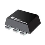
| 产品图片 |
|
| rohs | 符合RoHS无铅 / 符合限制有害物质指令(RoHS)规范要求 |
| 产品系列 | 逻辑集成电路,变换器,Texas Instruments SN74AHC1GU04DRLR74AHC |
| 数据手册 | |
| 产品型号 | SN74AHC1GU04DRLR |
| 不同V、最大CL时的最大传播延迟 | 7ns @ 5V,50pF |
| 产品种类 | 变换器 |
| 低电平输出电流 | 8 mA |
| 供应商器件封装 | SOT-5 |
| 其它名称 | 296-23234-6 |
| 包装 | Digi-Reel® |
| 单位重量 | 2.800 mg |
| 商标 | Texas Instruments |
| 安装类型 | 表面贴装 |
| 安装风格 | SMD/SMT |
| 封装 | Reel |
| 封装/外壳 | SOT-553 |
| 封装/箱体 | SOT-553-5 |
| 工作温度 | -40°C ~ 85°C |
| 工厂包装数量 | 4000 |
| 最大工作温度 | + 85 C |
| 标准包装 | 1 |
| 特性 | - |
| 电压-电源 | 2 V ~ 5.5 V |
| 电流-输出高,低 | 8mA,8mA |
| 电流-静态(最大值) | 1µA |
| 电源电压-最大 | 5.5 V |
| 电源电压-最小 | 2 V |
| 电路数 | 1 |
| 电路数量 | 1 Circuit |
| 系列 | SN74AHC1GU04 |
| 输入数 | 1 |
| 逻辑电平-低 | 0.3 V ~ 1.1 V |
| 逻辑电平-高 | 1.7 V ~ 4.4 V |
| 逻辑类型 | |
| 逻辑系列 | 74AHC |
| 高电平输出电流 | - 8 mA |


- 商务部:美国ITC正式对集成电路等产品启动337调查
- 曝三星4nm工艺存在良率问题 高通将骁龙8 Gen1或转产台积电
- 太阳诱电将投资9.5亿元在常州建新厂生产MLCC 预计2023年完工
- 英特尔发布欧洲新工厂建设计划 深化IDM 2.0 战略
- 台积电先进制程称霸业界 有大客户加持明年业绩稳了
- 达到5530亿美元!SIA预计今年全球半导体销售额将创下新高
- 英特尔拟将自动驾驶子公司Mobileye上市 估值或超500亿美元
- 三星加码芯片和SET,合并消费电子和移动部门,撤换高东真等 CEO
- 三星电子宣布重大人事变动 还合并消费电子和移动部门
- 海关总署:前11个月进口集成电路产品价值2.52万亿元 增长14.8%


PDF Datasheet 数据手册内容提取
Product Sample & Technical Tools & Support & Folder Buy Documents Software Community SN74AHC1GU04 SCLS343S–APRIL1996–REVISEDOCTOBER2016 SN74AHC1GU04 Single Inverter Gate 1 Features 2 Applications • OperatingRangeof2-Vto5.5-VV • WirelessandTelecomInfrastructure 1 CC • UnbufferedOutput • AudioMixers • ±8-mAOutputDriveat5V • TVs • Latch-UpPerformanceExceeds250mAPer • Set-Top-boxes JESD17 • Audio • ESDProtectionExceedsJESD22 • Servers – 2000-VHuman-BodyModel • Cameras:Surveillance – 200-VMachineModel • SoftwareDefinedRadio(SDR) – 1000-VCharged-DeviceModel 3 Description The SN74AHC1GU04 device contains a single inverter gate. The device performs the Boolean functionY= A. DeviceInformation(1) PARTNUMBER PACKAGE BODYSIZE(NOM) SN74AHC1GU04DBV SOT-23(5) 2.90mmx1.60mm SN74AHC1GU04DCK SC-70(5) 2.00mmx1.30mm SN74AHC1GU04DRL SOT(5) 1.65mmx1.20mm (1) For all available packages, see the orderable addendum at theendofthedatasheet. LogicDiagram(PositiveLogic) A Y Copyright © 2016,Texas Instruments Incorporated 1 An IMPORTANT NOTICE at the end of this data sheet addresses availability, warranty, changes, use in safety-critical applications, intellectualpropertymattersandotherimportantdisclaimers.PRODUCTIONDATA.
SN74AHC1GU04 SCLS343S–APRIL1996–REVISEDOCTOBER2016 www.ti.com Table of Contents 1 Features.................................................................. 1 8.2 FunctionalBlockDiagram.........................................8 2 Applications........................................................... 1 8.3 FeatureDescription...................................................8 3 Description............................................................. 1 8.4 DeviceFunctionalModes..........................................8 4 RevisionHistory..................................................... 2 9 ApplicationandImplementation.......................... 9 9.1 ApplicationInformation..............................................9 5 PinConfigurationandFunctions......................... 3 9.2 TypicalApplication....................................................9 6 Specifications......................................................... 4 10 PowerSupplyRecommendations..................... 10 6.1 AbsoluteMaximumRatings .....................................4 11 Layout................................................................... 11 6.2 ESDRatings..............................................................4 6.3 RecommendedOperatingConditions.......................4 11.1 LayoutGuidelines.................................................11 6.4 ThermalInformation..................................................5 11.2 LayoutExample....................................................11 6.5 ElectricalCharacteristics...........................................5 12 DeviceandDocumentationSupport................. 12 6.6 SwitchingCharacteristics,V =3.3V±0.3V........5 12.1 ReceivingNotificationofDocumentationUpdates12 CC 6.7 SwitchingCharacteristics,V =5V±0.5V...........5 12.2 CommunityResources..........................................12 CC 6.8 OperatingCharacteristics..........................................6 12.3 Trademarks...........................................................12 6.9 TypicalCharacteristics..............................................6 12.4 ElectrostaticDischargeCaution............................12 7 ParameterMeasurementInformation..................7 12.5 Glossary................................................................12 8 DetailedDescription.............................................. 8 13 Mechanical,Packaging,andOrderable Information........................................................... 12 8.1 Overview...................................................................8 4 Revision History NOTE:Pagenumbersforpreviousrevisionsmaydifferfrompagenumbersinthecurrentversion. ChangesfromRevisionR(December2014)toRevisionS Page • Deleted"2-Input"fromdatasheettitle................................................................................................................................... 1 • Addedmissingpackagenames.............................................................................................................................................. 1 • Changed"SOT-553"to"SOT" ............................................................................................................................................... 1 • Changed"I =50µA"to"I =50µA"forV inElectricalCharacteristicstable................................................................ 5 OH OL OL • ChangedTypicalApplicationSchematicwithamoreaccurateimage................................................................................... 9 • AddedReceivingNotificationofDocumentationUpdatessectionandCommunityResourcessection.............................. 12 ChangesfromRevisionQ(June2005)toRevisionR Page • AddedApplications,DeviceInformationtable,PinFunctionstable,ESDRatingstable,ThermalInformationtable, TypicalCharacteristics,FeatureDescriptionsection,DeviceFunctionalModes,ApplicationandImplementation section,PowerSupplyRecommendationssection,Layoutsection,DeviceandDocumentationSupportsection,and Mechanical,Packaging,andOrderableInformationsection.................................................................................................. 1 • DeletedOrderingInformationtable........................................................................................................................................ 1 • ChangedMAXoperatingtemperatureinRecommendedOperatingConditionstable.......................................................... 4 2 SubmitDocumentationFeedback Copyright©1996–2016,TexasInstrumentsIncorporated ProductFolderLinks:SN74AHC1GU04
SN74AHC1GU04 www.ti.com SCLS343S–APRIL1996–REVISEDOCTOBER2016 5 Pin Configuration and Functions DBVPackage 5-PinSOT-23 DRLPackage TopView 5-PinSOT TopView NC 1 5 VCC NC 1 5 VCC A 2 A 2 GND 3 4 Y GND 3 4 Y Not to scale Not to scale DCKPackage 5-PinSC70 TopView NC 1 5 VCC A 2 GND 3 4 Y Not to scale NC–Nointernalconnection Seemechanicaldrawingsfordimensions. PinFunctions PIN TYPE DESCRIPTION NO. NAME 1 NC — Noconnection 2 A I InputA 3 GND — Groundpin 4 Y O OutputY 5 V — Powerpin CC Copyright©1996–2016,TexasInstrumentsIncorporated SubmitDocumentationFeedback 3 ProductFolderLinks:SN74AHC1GU04
SN74AHC1GU04 SCLS343S–APRIL1996–REVISEDOCTOBER2016 www.ti.com 6 Specifications 6.1 Absolute Maximum Ratings overoperatingfree-airtemperaturerange(unlessotherwisenoted)(1) MIN MAX UNIT V Supplyvoltage –0.5 7 V CC V Inputvoltage (2) –0.5 7 V I V Outputvoltage (2) –0.5 V +0.5 V O CC I Inputclampcurrent V <0 –20 mA IK I I Outputclampcurrent V <0orV >V ±20 mA OK O O CC I Continuousoutputcurrent V =0toV ±25 mA O O CC ContinuouscurrentthrougheachV orGND ±50 mA CC T Junctiontemperature 150 °C J T Storagetemperature –65 150 °C stg (1) StressesbeyondthoselistedunderAbsoluteMaximumRatingsmaycausepermanentdamagetothedevice.Thesearestressratings only,andfunctionaloperationofthedeviceattheseoranyotherconditionsbeyondthoseindicatedunderRecommendedOperating Conditionsisnotimplied.Exposuretoabsolute-maximum-ratedconditionsforextendedperiodsmayaffectdevicereliability. (2) Theinputandoutputvoltageratingsmaybeexceedediftheinputandoutputcurrentratingsareobserved. 6.2 ESD Ratings VALUE UNIT Humanbodymodel(HBM),perANSI/ESDA/JEDECJS-001(1) 2000 V Electrostaticdischarge V (ESD) Chargeddevicemodel(CDM),perJEDECspecificationJESD22-C101(2) 1000 (1) JEDECdocumentJEP155statesthat500-VHBMallowssafemanufacturingwithastandardESDcontrolprocess. (2) JEDECdocumentJEP157statesthat250-VCDMallowssafemanufacturingwithastandardESDcontrolprocess. 6.3 Recommended Operating Conditions overoperatingfree-airtemperaturerange(unlessotherwisenoted)(1) MIN MAX UNIT V Supplyvoltage 2 5.5 V CC V =2V 1.7 CC V High-levelinputvoltage V =3V 2.4 V IH CC V =5.5V 4.4 CC V =2V 0.3 CC V Low-levelinputvoltage V =3V 0.6 V IL CC V =5.5V 1.1 CC V Inputvoltage 0 5.5 V IH V Outputvoltage 0 V V O CC V =2V –50 µA CC I High-leveloutputcurrent V =3.3V±0.3V –4 OH CC mA V =5V±0.5V –8 CC V =2V 50 µA CC I Low-leveloutputcurrent V =3.3V±0.3V 4 OL CC mA V =5V±0.5V 8 CC T Operatingfree-airtemperature –40 125 °C A (1) AllunusedinputsofthedevicemustbeheldatV orGNDtoensureproperdeviceoperation.SeeImplicationsofSloworFloating CC CMOSInputs(SCBA004). 4 SubmitDocumentationFeedback Copyright©1996–2016,TexasInstrumentsIncorporated ProductFolderLinks:SN74AHC1GU04
SN74AHC1GU04 www.ti.com SCLS343S–APRIL1996–REVISEDOCTOBER2016 6.4 Thermal Information SN74AHC1GU04 THERMALMETRIC(1) DBV DCK DRL UNIT (SOT-23) (SC70) (SOT) 5PINS R Junction-to-ambientthermalresistance 231.3 287.6 328.7 °C/W θJA R Junction-to-case(top)thermalresistance 119.9 97.7 105.1 °C/W θJC(top) R Junction-to-boardthermalresistance 60.6 65. 150.3 °C/W θJB ψ Junction-to-topcharacterizationparameter 17.8 2.0 6.9 °C/W JT ψ Junction-to-boardcharacterizationparameter 60.1 64.2 148.4 °C/W JB (1) Formoreinformationabouttraditionalandnewthermalmetrics,seetheSemiconductorandICPackageThermalMetricsapplication report. 6.5 Electrical Characteristics overoperatingfree-airtemperaturerange(unlessotherwisenoted) T =25°C –40°Cto+85°C –40°Cto+125°C A PARAMETER TESTCONDITIONS V UNIT CC MIN TYP MAX MIN MAX MIN MAX 2V 1.8 2 1.8 1.9 I =–50µA 3V 2.7 3 2.7 2.7 OH V 4.5V 4 4.5 4 4.4 V OH I =–4mA 3V 2.58 2.48 2.48 OH I =–8mA 4.5V 3.94 3.8 3.8 OH 2V 0.2 0.2 0.1 I =50µA 3V 0.3 0.3 0.1 OL V 4.5V 0.5 0.5 0.1 V OL I =4mA 3V 0.36 0.44 0.44 OL I =8mA 4.5V 0.36 0.44 0.44 OL 0Vto I V =5.5VorGND ±0.1 ±1 ±1 µA I I 5.5V I V =V orGND,I =0 5.5V 1 10 10 µA CC I CC O C V =V orGND 5V 2 10 10 10 pF i I CC 6.6 Switching Characteristics, V = 3.3 V ± 0.3 V CC overrecommendedoperatingfree-airtemperaturerange(unlessotherwisenoted)(seeFigure3) –40°Cto PARAMETER FROM TO OUTPUT TA=25°C +85°C –40°Cto+125°C UNIT (INPUT) (OUTPUT) CAPACITANCE MIN TYP MAX MIN MAX MIN MAX t 5 7.1 1 8.5 1 9.5 PLH A Y C =15pF ns L t 5 7.1 1 8.5 1 9.5 PHL t 7.5 10.6 1 12 1 13 PLH A Y C =50pF ns L t 7.5 10.6 1 12 1 13 PHL 6.7 Switching Characteristics, V = 5 V ± 0.5 V CC overrecommendedoperatingfree-airtemperaturerange(unlessotherwisenoted)(seeFigure3) –40°Cto PARAMETER FROM TO OUTPUT TA=25°C +85°C –40°Cto+125°C UNIT (INPUT) (OUTPUT) CAPACITANCE MIN TYP MAX MIN MAX MIN MAX t 3.5 5.5 1 6 1 6.5 PLH A Y C =15pF ns L t 3.5 5.5 1 6 1 6.5 PHL Copyright©1996–2016,TexasInstrumentsIncorporated SubmitDocumentationFeedback 5 ProductFolderLinks:SN74AHC1GU04
SN74AHC1GU04 SCLS343S–APRIL1996–REVISEDOCTOBER2016 www.ti.com Switching Characteristics, V = 5 V ± 0.5 V (continued) CC overrecommendedoperatingfree-airtemperaturerange(unlessotherwisenoted)(seeFigure3) –40°Cto PARAMETER FROM TO OUTPUT TA=25°C +85°C –40°Cto+125°C UNIT (INPUT) (OUTPUT) CAPACITANCE MIN TYP MAX MIN MAX MIN MAX t 5 7 1 8 1 8.5 PLH A Y C =50pF ns L t 5 7 1 8 1 8.5 PHL 6.8 Operating Characteristics V =5V,T =25°C CC A PARAMETER TESTCONDITIONS TYP UNIT C Powerdissipationcapacitance Noload, f=1MHz 7.3 pF pd 6.9 Typical Characteristics 4.5 7 4 6 3.5 5 3 ns) 2.5 ns) 4 D ( D ( TP 2 TP 3 1.5 2 1 1 0.5 TPD in ns TPD in ns 0 0 -100 -50 0 50 100 150 0 1 2 3 4 5 6 Temperature (qC) D001 VCC D002 Figure1.TPDvsTemperature Figure2.TPDvsV at25°C CC 6 SubmitDocumentationFeedback Copyright©1996–2016,TexasInstrumentsIncorporated ProductFolderLinks:SN74AHC1GU04
SN74AHC1GU04 www.ti.com SCLS343S–APRIL1996–REVISEDOCTOBER2016 7 Parameter Measurement Information VCC From Output Test From Output RL= 1 kΩ S1 Open TEST S1 UnderTest Point UnderTest GND tPLH/tPHL Open CL CL tPLZ/tPZL VCC (see NoteA) (see NoteA) tPHZ/tPZH GND Open Drain VCC LOAD CIRCUIT FOR LOAD CIRCUIT FOR TOTEM-POLE OUTPUTS 3-STATEAND OPEN-DRAIN OUTPUTS VCC Timing Input 50% VCC tw th 0 V VCC tsu VCC Input 50% VCC 50% VCC Data Input 50% VCC 50% VCC 0 V 0 V VOLTAGEWAVEFORMS VOLTAGEWAVEFORMS PULSEDURATION SETUPAND HOLD TIMES VCC VCC Output Input 50% VCC 50% VCC Control 50% VCC 50% VCC 0 V 0 V tPLH tPHL tPZL tPLZ Output VOH Waveform 1 ≈VCC InO-Puhtapsuet 50%VCC 50% VCC S1 at VCC 50% VCC VOL+0.3V VOL (see Note B) VOL tPHL tPLH tPZH tPHZ Output Out-ofO-Puhtapsuet 50% VCC 50% VCVVCOOHL (WseSae1v eNaftoo GtremN B D2) 50% VCC VOH−0.3VV≈0O VH VOLTAGEWAVEFORMS VOLTAGEWAVEFORMS PROPAGATIONDELAYTIMES ENABLEAND DISABLE TIMES INVERTINGAND NONINVERTING OUTPUTS LOW-AND HIGH-LEVELENABLING NOTES: A. CLincludes probe and jig capacitance. B. Waveform 1 is for an output with internal conditions such that the output is low except when disabled by the output control. Waveform 2 is for an output with internal conditions such that the output is high except when disabled by the output control. C. All input pulses are supplied by generators having the following characteristics: PRR≤1 MHz, ZO= 50Ω, tr≤3ns,tf≤3 ns. D. Theoutputsaremeasuredoneatatimewithoneinputtransitionpermeasurement. Figure3. LoadCircuitAndVoltageWaveforms Copyright©1996–2016,TexasInstrumentsIncorporated SubmitDocumentationFeedback 7 ProductFolderLinks:SN74AHC1GU04
SN74AHC1GU04 SCLS343S–APRIL1996–REVISEDOCTOBER2016 www.ti.com 8 Detailed Description 8.1 Overview The SN74AHC1GU04 device contains a single inverter gate. The device performs the Boolean function Y = A. Internal circuitry consists of a single-stage inverter that can be used in analog applications, such as crystal oscillators. 8.2 Functional Block Diagram A Y Copyright © 2016,Texas Instruments Incorporated Figure4. LogicDiagram(PositiveLogic) 8.3 Feature Description • Wideoperatingvoltagerange – Operatesfrom2Vto5.5V • Allowsdown-voltagetranslation – Inputsacceptvoltagesto5.5V • Theunbufferedoutputisidealforuseinoscillatorcircuits 8.4 Device Functional Modes Table1liststhefunctionalmodesofSN74AHC1GU04. Table1.FunctionTable INPUT OUTPUT A Y H L L H 8 SubmitDocumentationFeedback Copyright©1996–2016,TexasInstrumentsIncorporated ProductFolderLinks:SN74AHC1GU04
SN74AHC1GU04 www.ti.com SCLS343S–APRIL1996–REVISEDOCTOBER2016 9 Application and Implementation NOTE Information in the following applications sections is not part of the TI component specification, and TI does not warrant its accuracy or completeness. TI’s customers are responsible for determining suitability of components for their purposes. Customers should validateandtesttheirdesignimplementationtoconfirmsystemfunctionality. 9.1 Application Information A CMOS inverter is used as a linear amplifier in oscillator applications. Similar to a conventional amplifier, their open-loop gain is a critical characteristic. The bandwidth of an inverter decreases as the operating voltage decreases.Theopen-loopgainoftheAHC1GU04deviceisshowninFigure6. 9.2 Typical Application RF CMOS Inverter C1 Crystal C2 Copyright © 2016,Texas Instruments Incorporated Figure5. TypicalApplicationSchematic 9.2.1 DesignRequirements ThisdeviceusesCMOStechnologyandhasbalancedoutputdrive.Takecaretoavoidbuscontentionbecauseit can drive currents that would exceed maximum limits. The high drive will also create fast edges into light loads, soroutingandloadconditionsshouldbeconsideredtopreventringing. 9.2.2 DetailedDesignProcedure 1. RecommendedInputConditions – Forrisetimeandfalltimespecifications,see Δt/ΔVintheRecommendedOperatingConditions table. – ForspecifiedHighandlowlevels,seeV andV intheRecommendedOperatingConditions table. IH IL – Inputsareovervoltagetolerantallowingthemtogoashighas5.5VatanyvalidV . CC 2. RecommendedOutputConditions – Loadcurrentsshouldnotexceed25mAperoutputand50mAtotalforthepart. – OutputsshouldnotbepulledaboveV . CC Copyright©1996–2016,TexasInstrumentsIncorporated SubmitDocumentationFeedback 9 ProductFolderLinks:SN74AHC1GU04
SN74AHC1GU04 SCLS343S–APRIL1996–REVISEDOCTOBER2016 www.ti.com Typical Application (continued) 9.2.3 ApplicationCurve Figure6.Open-LoopGain 10 Power Supply Recommendations The power supply can be any voltage between the MIN and MAX supply voltage rating located in the RecommendedOperatingConditionstable. Each V pin should have a good bypass capacitor to prevent power disturbance. For devices with a single CC supply, 0.1 μF is recommended. If there are multiple V pins, 0.01 μF or 0.022 μF is recommended for each CC power pin. It is acceptable to parallel multiple bypass caps to reject different frequencies of noise. A 0.1 μF and 1 μF are commonly used in parallel. The bypass capacitor should be installed as close to the power pin as possibleforbestresults. 10 SubmitDocumentationFeedback Copyright©1996–2016,TexasInstrumentsIncorporated ProductFolderLinks:SN74AHC1GU04
SN74AHC1GU04 www.ti.com SCLS343S–APRIL1996–REVISEDOCTOBER2016 11 Layout 11.1 Layout Guidelines When using multiple bit logic devices, inputs should not float. In many cases, functions or parts of functions of digital logic devices are unused. Some examples are when only two inputs of a triple-input AND gate are used, or when only 3 of the 4-buffer gates are used. Such input pins should not be left unconnected because the undefinedvoltagesattheoutsideconnectionsresultinundefinedoperationalstates. Specified inFigure 7 are rules that must be observed under all circumstances. All unused inputs of digital logic devices must be connected to a high or low bias to prevent them from floating. The logic level that should be applied to any particular unused input depends on the function of the device. Generally they will be tied to GND or V , whichever makes more sense or is more convenient. It is acceptable to float outputs unless the part is a CC transceiver. If the transceiver has an output enable pin, it will disable the outputs section of the part when asserted.ThiswillnotdisabletheinputsectionoftheI/Ossotheyalsocannotfloatwhendisabled. 11.2 Layout Example V cc Input Unused Input Output Unused Input Output Input Figure7. LayoutDiagram Copyright©1996–2016,TexasInstrumentsIncorporated SubmitDocumentationFeedback 11 ProductFolderLinks:SN74AHC1GU04
SN74AHC1GU04 SCLS343S–APRIL1996–REVISEDOCTOBER2016 www.ti.com 12 Device and Documentation Support 12.1 Receiving Notification of Documentation Updates To receive notification of documentation updates, navigate to the device product folder on ti.com. In the upper right corner, click on Alert me to register and receive a weekly digest of any product information that has changed.Forchangedetails,reviewtherevisionhistoryincludedinanyreviseddocument. 12.2 Community Resources The following links connect to TI community resources. Linked contents are provided "AS IS" by the respective contributors. They do not constitute TI specifications and do not necessarily reflect TI's views; see TI's Terms of Use. TIE2E™OnlineCommunity TI'sEngineer-to-Engineer(E2E)Community.Createdtofostercollaboration amongengineers.Ate2e.ti.com,youcanaskquestions,shareknowledge,exploreideasandhelp solveproblemswithfellowengineers. DesignSupport TI'sDesignSupport QuicklyfindhelpfulE2Eforumsalongwithdesignsupporttoolsand contactinformationfortechnicalsupport. 12.3 Trademarks E2EisatrademarkofTexasInstruments. Allothertrademarksarethepropertyoftheirrespectiveowners. 12.4 Electrostatic Discharge Caution Thesedeviceshavelimitedbuilt-inESDprotection.Theleadsshouldbeshortedtogetherorthedeviceplacedinconductivefoam duringstorageorhandlingtopreventelectrostaticdamagetotheMOSgates. 12.5 Glossary SLYZ022—TIGlossary. Thisglossarylistsandexplainsterms,acronyms,anddefinitions. 13 Mechanical, Packaging, and Orderable Information The following pages include mechanical, packaging, and orderable information. This information is the most current data available for the designated devices. This data is subject to change without notice and revision of thisdocument.Forbrowser-basedversionsofthisdatasheet,refertotheleft-handnavigation. 12 SubmitDocumentationFeedback Copyright©1996–2016,TexasInstrumentsIncorporated ProductFolderLinks:SN74AHC1GU04
PACKAGE OPTION ADDENDUM www.ti.com 6-Feb-2020 PACKAGING INFORMATION Orderable Device Status Package Type Package Pins Package Eco Plan Lead/Ball Finish MSL Peak Temp Op Temp (°C) Device Marking Samples (1) Drawing Qty (2) (6) (3) (4/5) 74AHC1GU04DBVRG4 ACTIVE SOT-23 DBV 5 3000 Green (RoHS NIPDAU Level-1-260C-UNLIM -40 to 125 AU4G & no Sb/Br) 74AHC1GU04DBVTG4 ACTIVE SOT-23 DBV 5 250 Green (RoHS NIPDAU Level-1-260C-UNLIM -40 to 125 AU4G & no Sb/Br) 74AHC1GU04DCKTG4 ACTIVE SC70 DCK 5 250 Green (RoHS NIPDAU Level-1-260C-UNLIM -40 to 125 AD3 & no Sb/Br) SN74AHC1GU04DBVR ACTIVE SOT-23 DBV 5 3000 Green (RoHS NIPDAU | SN Level-1-260C-UNLIM -40 to 125 (AU43, AU4G, AU4J, & no Sb/Br) AU4L, AU4S) SN74AHC1GU04DBVT ACTIVE SOT-23 DBV 5 250 Green (RoHS NIPDAU | SN Level-1-260C-UNLIM -40 to 125 (AU43, AU4G, AU4J, & no Sb/Br) AU4L, AU4S) SN74AHC1GU04DCK3 ACTIVE SC70 DCK 5 3000 Pb-Free SNBI Level-1-260C-UNLIM -40 to 85 ADY (RoHS) SN74AHC1GU04DCKR ACTIVE SC70 DCK 5 3000 Green (RoHS NIPDAU | SN Level-1-260C-UNLIM -40 to 125 (AD3, ADG, ADJ, AD & no Sb/Br) L, ADS) SN74AHC1GU04DCKT ACTIVE SC70 DCK 5 250 Green (RoHS NIPDAU | SN Level-1-260C-UNLIM -40 to 125 (AD3, ADG, ADJ, AD & no Sb/Br) L, ADS) SN74AHC1GU04DRLR ACTIVE SOT-5X3 DRL 5 4000 Green (RoHS NIPDAUAG Level-1-260C-UNLIM -40 to 125 ADS & no Sb/Br) (1) The marketing status values are defined as follows: ACTIVE: Product device recommended for new designs. LIFEBUY: TI has announced that the device will be discontinued, and a lifetime-buy period is in effect. NRND: Not recommended for new designs. Device is in production to support existing customers, but TI does not recommend using this part in a new design. PREVIEW: Device has been announced but is not in production. Samples may or may not be available. OBSOLETE: TI has discontinued the production of the device. (2) RoHS: TI defines "RoHS" to mean semiconductor products that are compliant with the current EU RoHS requirements for all 10 RoHS substances, including the requirement that RoHS substance do not exceed 0.1% by weight in homogeneous materials. Where designed to be soldered at high temperatures, "RoHS" products are suitable for use in specified lead-free processes. TI may reference these types of products as "Pb-Free". RoHS Exempt: TI defines "RoHS Exempt" to mean products that contain lead but are compliant with EU RoHS pursuant to a specific EU RoHS exemption. Green: TI defines "Green" to mean the content of Chlorine (Cl) and Bromine (Br) based flame retardants meet JS709B low halogen requirements of <=1000ppm threshold. Antimony trioxide based flame retardants must also meet the <=1000ppm threshold requirement. (3) MSL, Peak Temp. - The Moisture Sensitivity Level rating according to the JEDEC industry standard classifications, and peak solder temperature. Addendum-Page 1
PACKAGE OPTION ADDENDUM www.ti.com 6-Feb-2020 (4) There may be additional marking, which relates to the logo, the lot trace code information, or the environmental category on the device. (5) Multiple Device Markings will be inside parentheses. Only one Device Marking contained in parentheses and separated by a "~" will appear on a device. If a line is indented then it is a continuation of the previous line and the two combined represent the entire Device Marking for that device. (6) Lead/Ball Finish - Orderable Devices may have multiple material finish options. Finish options are separated by a vertical ruled line. Lead/Ball Finish values may wrap to two lines if the finish value exceeds the maximum column width. Important Information and Disclaimer:The information provided on this page represents TI's knowledge and belief as of the date that it is provided. TI bases its knowledge and belief on information provided by third parties, and makes no representation or warranty as to the accuracy of such information. Efforts are underway to better integrate information from third parties. TI has taken and continues to take reasonable steps to provide representative and accurate information but may not have conducted destructive testing or chemical analysis on incoming materials and chemicals. TI and TI suppliers consider certain information to be proprietary, and thus CAS numbers and other limited information may not be available for release. In no event shall TI's liability arising out of such information exceed the total purchase price of the TI part(s) at issue in this document sold by TI to Customer on an annual basis. Addendum-Page 2
PACKAGE MATERIALS INFORMATION www.ti.com 24-Apr-2020 TAPE AND REEL INFORMATION *Alldimensionsarenominal Device Package Package Pins SPQ Reel Reel A0 B0 K0 P1 W Pin1 Type Drawing Diameter Width (mm) (mm) (mm) (mm) (mm) Quadrant (mm) W1(mm) 74AHC1GU04DBVRG4 SOT-23 DBV 5 3000 178.0 9.0 3.23 3.17 1.37 4.0 8.0 Q3 74AHC1GU04DBVTG4 SOT-23 DBV 5 250 178.0 9.0 3.23 3.17 1.37 4.0 8.0 Q3 74AHC1GU04DCKTG4 SC70 DCK 5 250 178.0 9.2 2.4 2.4 1.22 4.0 8.0 Q3 SN74AHC1GU04DBVR SOT-23 DBV 5 3000 180.0 8.4 3.23 3.17 1.37 4.0 8.0 Q3 SN74AHC1GU04DBVR SOT-23 DBV 5 3000 178.0 9.2 3.3 3.23 1.55 4.0 8.0 Q3 SN74AHC1GU04DBVR SOT-23 DBV 5 3000 178.0 9.0 3.3 3.2 1.4 4.0 8.0 Q3 SN74AHC1GU04DBVR SOT-23 DBV 5 3000 178.0 9.0 3.3 3.2 1.4 4.0 8.0 Q3 SN74AHC1GU04DBVT SOT-23 DBV 5 250 178.0 9.0 3.23 3.17 1.37 4.0 8.0 Q3 SN74AHC1GU04DBVT SOT-23 DBV 5 250 180.0 8.4 3.23 3.17 1.37 4.0 8.0 Q3 SN74AHC1GU04DBVT SOT-23 DBV 5 250 178.0 9.0 3.3 3.2 1.4 4.0 8.0 Q3 SN74AHC1GU04DBVT SOT-23 DBV 5 250 178.0 9.2 3.3 3.23 1.55 4.0 8.0 Q3 SN74AHC1GU04DCKR SC70 DCK 5 3000 178.0 9.0 2.4 2.5 1.2 4.0 8.0 Q3 SN74AHC1GU04DCKR SC70 DCK 5 3000 178.0 9.0 2.4 2.5 1.2 4.0 8.0 Q3 SN74AHC1GU04DCKR SC70 DCK 5 3000 180.0 8.4 2.47 2.3 1.25 4.0 8.0 Q3 SN74AHC1GU04DCKR SC70 DCK 5 3000 178.0 9.2 2.4 2.4 1.22 4.0 8.0 Q3 SN74AHC1GU04DCKT SC70 DCK 5 250 178.0 9.2 2.4 2.4 1.22 4.0 8.0 Q3 SN74AHC1GU04DCKT SC70 DCK 5 250 178.0 9.0 2.4 2.5 1.2 4.0 8.0 Q3 SN74AHC1GU04DCKT SC70 DCK 5 250 178.0 9.0 2.4 2.5 1.2 4.0 8.0 Q3 PackMaterials-Page1
PACKAGE MATERIALS INFORMATION www.ti.com 24-Apr-2020 Device Package Package Pins SPQ Reel Reel A0 B0 K0 P1 W Pin1 Type Drawing Diameter Width (mm) (mm) (mm) (mm) (mm) Quadrant (mm) W1(mm) SN74AHC1GU04DRLR SOT-5X3 DRL 5 4000 180.0 8.4 1.98 1.78 0.69 4.0 8.0 Q3 *Alldimensionsarenominal Device PackageType PackageDrawing Pins SPQ Length(mm) Width(mm) Height(mm) 74AHC1GU04DBVRG4 SOT-23 DBV 5 3000 180.0 180.0 18.0 74AHC1GU04DBVTG4 SOT-23 DBV 5 250 180.0 180.0 18.0 74AHC1GU04DCKTG4 SC70 DCK 5 250 180.0 180.0 18.0 SN74AHC1GU04DBVR SOT-23 DBV 5 3000 202.0 201.0 28.0 SN74AHC1GU04DBVR SOT-23 DBV 5 3000 180.0 180.0 18.0 SN74AHC1GU04DBVR SOT-23 DBV 5 3000 180.0 180.0 18.0 SN74AHC1GU04DBVR SOT-23 DBV 5 3000 180.0 180.0 18.0 SN74AHC1GU04DBVT SOT-23 DBV 5 250 180.0 180.0 18.0 SN74AHC1GU04DBVT SOT-23 DBV 5 250 202.0 201.0 28.0 SN74AHC1GU04DBVT SOT-23 DBV 5 250 180.0 180.0 18.0 SN74AHC1GU04DBVT SOT-23 DBV 5 250 180.0 180.0 18.0 SN74AHC1GU04DCKR SC70 DCK 5 3000 180.0 180.0 18.0 SN74AHC1GU04DCKR SC70 DCK 5 3000 180.0 180.0 18.0 SN74AHC1GU04DCKR SC70 DCK 5 3000 202.0 201.0 28.0 SN74AHC1GU04DCKR SC70 DCK 5 3000 180.0 180.0 18.0 SN74AHC1GU04DCKT SC70 DCK 5 250 180.0 180.0 18.0 PackMaterials-Page2
PACKAGE MATERIALS INFORMATION www.ti.com 24-Apr-2020 Device PackageType PackageDrawing Pins SPQ Length(mm) Width(mm) Height(mm) SN74AHC1GU04DCKT SC70 DCK 5 250 180.0 180.0 18.0 SN74AHC1GU04DCKT SC70 DCK 5 250 180.0 180.0 18.0 SN74AHC1GU04DRLR SOT-5X3 DRL 5 4000 202.0 201.0 28.0 PackMaterials-Page3
None
None
PACKAGE OUTLINE DBV0005A SOT-23 - 1.45 mm max height SCALE 4.000 SMALL OUTLINE TRANSISTOR C 3.0 2.6 0.1 C 1.75 1.45 1.45 B A 0.90 PIN 1 INDEX AREA 1 5 2X 0.95 3.05 2.75 1.9 1.9 2 4 3 0.5 5X 0.3 0.15 0.2 C A B (1.1) TYP 0.00 0.25 GAGE PLANE 0.22 TYP 0.08 8 TYP 0.6 0 0.3 TYP SEATING PLANE 4214839/E 09/2019 NOTES: 1. All linear dimensions are in millimeters. Any dimensions in parenthesis are for reference only. Dimensioning and tolerancing per ASME Y14.5M. 2. This drawing is subject to change without notice. 3. Refernce JEDEC MO-178. 4. Body dimensions do not include mold flash, protrusions, or gate burrs. Mold flash, protrusions, or gate burrs shall not exceed 0.15 mm per side. www.ti.com
EXAMPLE BOARD LAYOUT DBV0005A SOT-23 - 1.45 mm max height SMALL OUTLINE TRANSISTOR PKG 5X (1.1) 1 5 5X (0.6) SYMM (1.9) 2 2X (0.95) 3 4 (R0.05) TYP (2.6) LAND PATTERN EXAMPLE EXPOSED METAL SHOWN SCALE:15X SOLDER MASK SOLDER MASK METAL UNDER METAL OPENING OPENING SOLDER MASK EXPOSED METAL EXPOSED METAL 0.07 MAX 0.07 MIN ARROUND ARROUND NON SOLDER MASK SOLDER MASK DEFINED DEFINED (PREFERRED) SOLDER MASK DETAILS 4214839/E 09/2019 NOTES: (continued) 5. Publication IPC-7351 may have alternate designs. 6. Solder mask tolerances between and around signal pads can vary based on board fabrication site. www.ti.com
EXAMPLE STENCIL DESIGN DBV0005A SOT-23 - 1.45 mm max height SMALL OUTLINE TRANSISTOR PKG 5X (1.1) 1 5 5X (0.6) SYMM 2 (1.9) 2X(0.95) 3 4 (R0.05) TYP (2.6) SOLDER PASTE EXAMPLE BASED ON 0.125 mm THICK STENCIL SCALE:15X 4214839/E 09/2019 NOTES: (continued) 7. Laser cutting apertures with trapezoidal walls and rounded corners may offer better paste release. IPC-7525 may have alternate design recommendations. 8. Board assembly site may have different recommendations for stencil design. www.ti.com
None
None
IMPORTANTNOTICEANDDISCLAIMER TI PROVIDES TECHNICAL AND RELIABILITY DATA (INCLUDING DATASHEETS), DESIGN RESOURCES (INCLUDING REFERENCE DESIGNS), APPLICATION OR OTHER DESIGN ADVICE, WEB TOOLS, SAFETY INFORMATION, AND OTHER RESOURCES “AS IS” AND WITH ALL FAULTS, AND DISCLAIMS ALL WARRANTIES, EXPRESS AND IMPLIED, INCLUDING WITHOUT LIMITATION ANY IMPLIED WARRANTIES OF MERCHANTABILITY, FITNESS FOR A PARTICULAR PURPOSE OR NON-INFRINGEMENT OF THIRD PARTY INTELLECTUAL PROPERTY RIGHTS. These resources are intended for skilled developers designing with TI products. You are solely responsible for (1) selecting the appropriate TI products for your application, (2) designing, validating and testing your application, and (3) ensuring your application meets applicable standards, and any other safety, security, or other requirements. These resources are subject to change without notice. TI grants you permission to use these resources only for development of an application that uses the TI products described in the resource. Other reproduction and display of these resources is prohibited. No license is granted to any other TI intellectual property right or to any third party intellectual property right. TI disclaims responsibility for, and you will fully indemnify TI and its representatives against, any claims, damages, costs, losses, and liabilities arising out of your use of these resources. TI’s products are provided subject to TI’s Terms of Sale (www.ti.com/legal/termsofsale.html) or other applicable terms available either on ti.com or provided in conjunction with such TI products. TI’s provision of these resources does not expand or otherwise alter TI’s applicable warranties or warranty disclaimers for TI products. Mailing Address: Texas Instruments, Post Office Box 655303, Dallas, Texas 75265 Copyright © 2020, Texas Instruments Incorporated