ICGOO在线商城 > 集成电路(IC) > 逻辑 - 信号开关,多路复用器,解码器 > SN74AHC157DBR

 Datasheet下载
- 型号: SN74AHC157DBR
- 制造商: Texas Instruments
- 库位|库存: xxxx|xxxx
- 要求:
| 数量阶梯 | 香港交货 | 国内含税 |
| +xxxx | $xxxx | ¥xxxx |
查看当月历史价格
查看今年历史价格
SN74AHC157DBR产品简介:
ICGOO电子元器件商城为您提供SN74AHC157DBR由Texas Instruments设计生产,在icgoo商城现货销售,并且可以通过原厂、代理商等渠道进行代购。 SN74AHC157DBR价格参考¥0.93-¥2.65。Texas InstrumentsSN74AHC157DBR封装/规格:逻辑 - 信号开关,多路复用器,解码器, Multiplexer 4 x 2:1 16-SSOP。您可以下载SN74AHC157DBR参考资料、Datasheet数据手册功能说明书,资料中有SN74AHC157DBR 详细功能的应用电路图电压和使用方法及教程。
SN74AHC157DBR 是由 Texas Instruments(德州仪器)生产的一款双四路数据选择器/多路复用器(2:1 Multiplexer),属于逻辑 - 信号开关、多路复用器和解码器类别的产品。以下是其典型应用场景:

 1. 数字信号切换
   SN74AHC157DBR 可用于在两个不同的输入信号之间进行选择,将其中一个信号传递到输出端。这种功能适用于需要动态切换信号的场景,例如:
   - 在音频系统中切换不同的音源输入。
   - 在视频处理设备中切换不同摄像头或显示器的信号。

 2. 数据路径控制
   在微处理器或 FPGA 系统中,SN74AHC157DBR 可以用来控制数据流的方向。例如:
   - 在数据总线设计中,选择不同的外设或存储器作为数据源。
   - 实现多任务处理中的资源共享,减少硬件资源的占用。

 3. 测试与测量设备
   在自动化测试设备(ATE)中,SN74AHC157DBR 能够实现对多个传感器或信号源的快速切换,从而提高测试效率。例如:
   - 切换不同通道的电压或电流信号进行测量。
   - 在示波器或多通道数据采集系统中选择目标信号。

 4. 通信接口设计
   该器件可以用于设计通信接口中的信号路由。例如:
   - 在 RS-232 或 SPI 接口中切换不同的设备连接。
   - 实现主从设备之间的信号切换,优化通信链路。

 5. 嵌入式系统中的信号管理
   在嵌入式控制系统中,SN74AHC157DBR 可以帮助管理复杂的信号网络。例如:
   - 切换 GPIO 引脚的功能,使其适应不同的工作模式。
   - 在工业控制中选择不同的输入/输出信号以适应实时需求。

 6. 低功耗应用
   由于 SN74AHC157DBR 具有低静态电流特性,适合用于电池供电设备中的信号切换。例如:
   - 在便携式医疗设备中切换传感器信号。
   - 在物联网(IoT)设备中优化信号路径以降低功耗。

 总结
SN74AHC157DBR 的主要应用场景集中在需要高效信号切换和数据路径控制的场合。它凭借其高可靠性、低功耗和快速响应时间,在消费电子、工业自动化、通信设备和测试测量等领域具有广泛的应用价值。
| 参数 | 数值 |
| 产品目录 | 集成电路 (IC)半导体 |
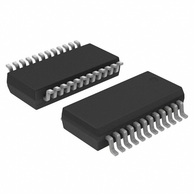
| 描述 | IC 2-1 QUAD SELECT/MUX 16-SSOP编码器、解码器、复用器和解复用器 Quad Data |
| 产品分类 | |
| 品牌 | Texas Instruments |
| 产品手册 | |
| 产品图片 |
|
| rohs | 符合RoHS无铅 / 符合限制有害物质指令(RoHS)规范要求 |
| 产品系列 | 逻辑集成电路,编码器、解码器、复用器和解复用器,Texas Instruments SN74AHC157DBR74AHC |
| 数据手册 | |
| 产品型号 | SN74AHC157DBR |
| 产品 | Selectors / Multiplexers |
| 产品种类 | 编码器、解码器、复用器和解复用器 |
| 传播延迟时间 | 13.2 ns at 3.3 V, 8.4 ns at 5 V |
| 位数 | 4 |
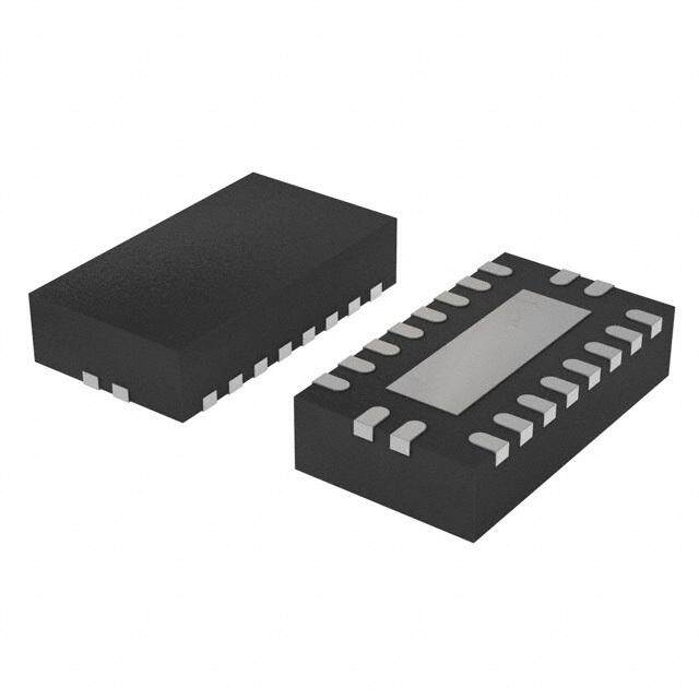
| 供应商器件封装 | 16-SSOP |
| 其它名称 | 296-4552-6 |
| 功率耗散 | 2.5 W |
| 包装 | Digi-Reel® |
| 单位重量 | 128.600 mg |
| 商标 | Texas Instruments |
| 安装类型 | 表面贴装 |
| 安装风格 | SMD/SMT |
| 封装 | Reel |
| 封装/外壳 | 16-SSOP(0.209",5.30mm 宽) |
| 封装/箱体 | SSOP-16 |
| 工作温度 | -40°C ~ 125°C |
| 工作温度范围 | - 40 C to + 85 C |
| 工作电压 | 2 V to 5.5 V |
| 工厂包装数量 | 2000 |
| 最大工作温度 | + 85 C |
| 最小工作温度 | - 40 C |
| 标准包装 | 1 |
| 独立电路 | 1 |
| 电压-电源 | 2 V ~ 5.5 V |
| 电压源 | 单电源 |
| 电流-输出高,低 | 8mA,8mA |
| 电源电压-最大 | 5.5 V |
| 电源电压-最小 | 2 V |
| 电路 | 4 x 2:1 |
| 类型 | 多路复用器 |
| 系列 | SN74AHC157 |
| 输入/输出线数量 | 2 / 1 |
| 输入线路数量 | 2 |
| 输出线路数量 | 1 |
| 逻辑系列 | AHC |


- 商务部:美国ITC正式对集成电路等产品启动337调查
- 曝三星4nm工艺存在良率问题 高通将骁龙8 Gen1或转产台积电
- 太阳诱电将投资9.5亿元在常州建新厂生产MLCC 预计2023年完工
- 英特尔发布欧洲新工厂建设计划 深化IDM 2.0 战略
- 台积电先进制程称霸业界 有大客户加持明年业绩稳了
- 达到5530亿美元!SIA预计今年全球半导体销售额将创下新高
- 英特尔拟将自动驾驶子公司Mobileye上市 估值或超500亿美元
- 三星加码芯片和SET,合并消费电子和移动部门,撤换高东真等 CEO
- 三星电子宣布重大人事变动 还合并消费电子和移动部门
- 海关总署:前11个月进口集成电路产品价值2.52万亿元 增长14.8%


PDF Datasheet 数据手册内容提取
SN54AHC157 SN74AHC157 www.ti.com SCLS345J–MAY1996–REVISEDJUNE2013 QUADRUPLE 2-LINE TO 1-LINE DATA SELECTORS/MULTIPLEXERS CheckforSamples:SN54AHC157,SN74AHC157 FEATURES 1 • OperatingRange2-Vto5.5-V • ESDProtectionExceedsJESD22 • Latch-UpPerformanceExceeds250mAPer – 2000-VHuman-BodyModel(A114-A) JESD17 – 200-VMachineModel(A115-A) – 1000-VCharged-DeviceModel(C101) SN54AHC157 . . . J or W PACKAGE SN74AHC157...RGY PACKAGE SN54AHC157...FKPACKAGE SN74AHC157...D,DB,DGV,N,NS, (TOPVIEW) (TOPVIEW) ORPWPACKAGE (TOPVIEW) A/B VCC 1A A/B NCVCCG A/B 1 16 VCC 1 16 3 2 1 20 19 1A 2 15 G 1A 2 15 G 1B 4 18 4A 1B 3 14 4A 1B 3 14 4A 1Y 5 17 4B 1Y 4 13 4B 1Y 4 13 4B NC 6 16 NC 2A 5 12 4Y 2A 5 12 4Y 2A 7 15 4Y 2B 6 11 3A 2B 6 11 3A 2B 8 14 3A 9 10 11 12 13 2Y 7 10 3B 2Y 7 10 3B 8 9 GND 8 9 3Y Y D CY B 2 N N3 3 D Y G N 3 G NC−No internal connection DESCRIPTION Thesequadruple2-lineto1-linedataselectors/multiplexersaredesignedfor2-Vto5.5-VV operation. CC The ’AHC157 devices feature a common strobe (G) input. When the strobe is high, all outputs are low. When the strobe is low, a 4-bit word is selected from one of two sources and is routed to the four outputs. The devices providetruedata. FUNCTIONTABLE INPUTS OUTP UT G A/B A B Y H X X X L L L L X L L L H X H L H X L L L H X H H 1 Pleasebeawarethatanimportantnoticeconcerningavailability,standardwarranty,anduseincriticalapplicationsof TexasInstrumentssemiconductorproductsanddisclaimerstheretoappearsattheendofthisdatasheet. PRODUCTIONDATAinformationiscurrentasofpublicationdate. Copyright©1996–2013,TexasInstrumentsIncorporated Products conform to specifications per the terms of the Texas Instruments standard warranty. Production processing does not necessarilyincludetestingofallparameters.
SN54AHC157 SN74AHC157 SCLS345J–MAY1996–REVISEDJUNE2013 www.ti.com LOGICDIAGRAM(POSITIVELOGIC) 2 1A 4 1Y 3 1B 5 2A 7 2Y 6 2B 11 3A 9 3Y 10 3B 14 4A 12 4Y 13 4B 15 G 1 A/B PinnumbersshownarefortheD,DB,DGV,J,N,NS,PW,RGY,andWpackages. 2 SubmitDocumentationFeedback Copyright©1996–2013,TexasInstrumentsIncorporated ProductFolderLinks:SN54AHC157SN74AHC157
SN54AHC157 SN74AHC157 www.ti.com SCLS345J–MAY1996–REVISEDJUNE2013 ABSOLUTE MAXIMUM RATINGS overoperatingfree-airtemperaturerange(unlessotherwisenoted)(1) VALUE UNIT Supplyvoltagerange,V –0.5to7 V CC Inputvoltagerange,V(2) –0.5to7 V I Outputvoltagerange,V (2) –0.5toV +0.5 V O CC Inputclampcurrent,I (V <0) –20 mA IK I Outputclampcurrent,I (V <0orV >V ) ±20 mA OK O O CC Continuousoutputcurrent,I (V =0toV ) ±25 mA O O CC ContinuouscurrentthroughV orGND ±50 mA CC Dpackage(3) 73 DBpackage(3) 82 DGVpackage(3) 120 Packagethermalimpedance,θ Npackage(3) 67 °C/W JA NSpackage(3) 64 PWpackage(3) 108 RGYpackage(4) 39 Storagetemperaturerange,T –65to150 °C stg (1) Stressesbeyondthoselistedunder“absolutemaximumratings”maycausepermanentdamagetothedevice.Thesearestressratings only,andfunctionaloperationofthedeviceattheseoranyotherconditionsbeyondthoseindicatedunder“recommendedoperating conditions”isnotimplied.Exposuretoabsolute-maximum-ratedconditionsforextendedperiodsmayaffectdevicereliability. (2) Theinputandoutputvoltageratingsmaybeexceedediftheinputandoutputcurrentratingsareobserved. (3) ThepackagethermalimpedanceiscalculatedinaccordancewithJESD51-7. (4) ThepackagethermalimpedanceiscalculatedinaccordancewithJESD51-5. RECOMMENDED OPERATING CONDITIONS(1) SN54AHC157 SN74AHC157 UNIT MIN MAX MIN MAX V Supplyvoltage 2 5.5 2 5.5 V CC V =2V 1.5 1.5 CC V High-levelinputvoltage V =3V 2.1 2.1 V IH CC V =5.5V 3.85 3.85 CC V =2V 0.5 0.5 CC V Low-levelInputvoltage V =3V 0.9 0.9 V IL CC V =5.5V 1.65 1.65 CC V Inputvoltage 0 5.5 0 5.5 V I V Outputvoltage 0 V 0 V V O CC CC V =2V –50 –50 CC I High-leveloutputcurrent V =3.3V±0.3V –4 –4 mA OH CC V =5V±0.5V –8 –8 CC V =2V 50 50 CC I Low-leveloutputcurrent V =3.3V±0.3V 4 4 mA OL CC V =5V±0.5V 8 8 CC V =3.3V±0.3V 100 100 CC Δt/Δv InputTransitionriseorfallrate ns/V V =5V±0.5V 20 20 CC T Operatingfree-airtemperature –55 125 –40 125 °C A (1) AllunusedinputsofthedevicemustbeheldatV orGNDtoensureproperdeviceoperation.RefertotheTIapplicationreport, CC ImplicationsofSloworFloatingCMOSInputs,literaturenumberSCBA004. Copyright©1996–2013,TexasInstrumentsIncorporated SubmitDocumentationFeedback 3 ProductFolderLinks:SN54AHC157SN74AHC157
SN54AHC157 SN74AHC157 SCLS345J–MAY1996–REVISEDJUNE2013 www.ti.com ELECTRICAL CHARACTERISTICS overoperatingfree-airtemperaturerange(unlessotherwisenoted) TA=–40°CTO TA=–55°CTO TA=–40°CTO 125°C PARAMETER TESTCONDITIONS VCC TA=25°C 125°C 85°C Recommended UNIT SN54AHC157 SN74AHC157 SN74AHC157 MIN TYP MAX MIN MAX MIN MAX MIN MAX 2V 1.9 2 1.9 1.9 1.9 IOH=–50µA 3V 2.9 3 2.9 2.9 2.9 VOH 4.5V 4.4 4.5 4.4 4.4 4.4 V IOH=–4mA 3V 2.58 2.48 2.48 2.48 IOH=–8mA 4.5V 3.94 3.8 3.8 3.8 2V 0.1 0.1 0.1 0.1 IOL=50µA 3V 0.1 0.1 0.1 0.1 VOL 4.5V 0.1 0.1 0.1 0.1 V IOH=4mA 3V 0.36 0.5 0.44 0.5 IOH=8mA 4.5V 0.36 0.5 0.44 0.5 II VI=5.5VorGND 0VtVo5.5 ±0.1 ±1(1) ±1 ±1 µA ICC VGIN=DV,CCor IO=0 5.5V 4 40 40 40 µA Ci VI=VCCorGND 5V 2 10 10 pF (1) OnproductscomplianttoMIL-PRF-38535,thisparameterisnotproductiontestedatVCC=0V. SWITCHING CHARACTERISTICS overrecommendedoperatingfree-airtemperaturerange,V =3.3V±0.3V(unlessotherwisenoted)(seeFigure1) CC TA=–40°CTO TA=–55°CTO TA=–40°CTO 125°C PARAMETER FROM TO LOAD TA=25°C 125°C 85°C Recommended UNIT (INPUT) (OUTPUT) CAPACITANCE SN54AHC157 SN74AHC157 SN74AHC157 TYP MAX MIN MAX MIN MAX MIN MAX tPLH 6.2(1) 9.7(1) 1(1) 11.5(1) 1 11.5 1 11.5 tPHL AorB Y CL=15pF 6.2(1) 9.7(1) 1(1) 11.5(1) 1 11.5 1 11.5 ns tPLH 8.4(1) 13.2(1) 1(1) 15.5(1) 1 15.5 1 15.5 tPHL A/B Y CL=15pF 8.4(1) 13.2(1) 1(1) 15.5(1) 1 15.5 1 15.5 ns tPLH 8.7(1) 13.6(1) 1(1) 16(1) 1 16 1 16 tPHL G Y CL=15pF 8.7(1) 13.6(1) 1(1) 16(1) 1 16 1 16 ns tPLH 8.7 13.2 1 15 1 15 1 15 AorB Y CL=50pF ns tPHL 8.7 13.2 1 15 1 15 1 15 tPLH 10.9 16.7 1 19 1 19 1 19 A/B Y CL=50pF ns tPHL 10.9 16.7 1 19 1 19 1 19 tPLH 11.2 17.1 1 19.5 1 19.5 1 19.5 G Y CL=50pF ns tPHL 11.2 17.1 1 19.5 1 19.5 1 19.5 (1) OnproductscomplianttoMIL-PRF-38535,thisparameterisnotproductiontested. 4 SubmitDocumentationFeedback Copyright©1996–2013,TexasInstrumentsIncorporated ProductFolderLinks:SN54AHC157SN74AHC157
SN54AHC157 SN74AHC157 www.ti.com SCLS345J–MAY1996–REVISEDJUNE2013 SWITCHING CHARACTERISTICS overrecommendedoperatingfree-airtemperaturerange,V =5V±0.5V(unlessotherwisenoted)(seeFigure1) CC TA=–40°CTO TA=–55°CTO TA=–40°CTO 125°C PARAMETER FROM TO LOAD TA=25°C 125°C 85°C Recommended UNIT (INPUT) (OUTPUT) CAPACITANCE SN54AHC157 SN74AHC157 SN74AHC157 TYP MAX MIN MAX MIN MAX MIN MAX tPLH 4.1(1) 6.4(1) 1(1) 7.5(1) 1 7.5 1 7.5 tPHL AorB Y CL=15pF 4.1(1) 6.4(1) 1(1) 7.5(1) 1 7.5 1 7.5 ns tPLH 5.3(1) 8.1(1) 1(1) 9.5(1) 1 9.5 1 9.5 tPHL A/B Y CL=15pF 5.3(1) 8.1(1) 1(1) 9.5(1) 1 9.5 1 9.5 ns tPLH 5.6(1) 8.6(1) 1(1) 10(1) 1 10 1 10 tPHL G Y CL=15pF 5.6(1) 8.6(1) 1(1) 10(1) 1 10 1 10 ns tPLH 5.6(1) 8.4(1) 1(1) 9.5(1) 1 9.5 1 9.5 tPHL AorB Y CL=50pF 5.6(1) 8.4(1) 1(1) 9.5(1) 1 9.5 1 9.5 ns tPLH 6.8(1) 10.1(1) 1(1) 11.5(1) 1 11.5 1 11.5 tPHL A/B Y CL=50pF 6.8(1) 10.1(1) 1(1) 11.5(1) 1 11.5 1 11.5 ns tPLH 7.1(1) 10.6(1) 1(1) 12(1) 1 12 1 12 tPHL G Y CL=50pF 7.1(1) 10.6(1) 1(1) 12(1) 1 12 1 12 ns (1) OnproductscomplianttoMIL-PRF-38535,thisparameterisnotproductiontested. NOISE CHARACTERISTICS V =5V,C =50pF,T =25°C(1) CC L A SN74AHC157 UNIT PARAMETER MIN TYP MAX V Quietoutput,maximumdynamicV 0.8 V OL(P) OL V Quietoutput,minimumdynamicV –0.8 V OL(V) OL V Quietoutput,minimumdynamicV 4.8 V OH(V) OH V High-leveldynamicinputvoltage 3.5 V IH(D) V Low-leveldynamicinputvoltage 1.5 V IL(D) (1) Characteristicsareforsurface-mountpackagesonly. OPERATING CHARACTERISTICS V =5V,T =25°C CC A PARAMETER TESTCONDITIONS TYP UNIT C Powerdissipationcapacitance Noload, f=1MHz 11 pF pd Copyright©1996–2013,TexasInstrumentsIncorporated SubmitDocumentationFeedback 5 ProductFolderLinks:SN54AHC157SN74AHC157
SN54AHC157 SN74AHC157 SCLS345J–MAY1996–REVISEDJUNE2013 www.ti.com PARAMETER MEASUREMENT INFORMATION VCC FromOutput Test FromOutput RL=1kΩ S1 Open TEST S1 UnderTest Point UnderTest GND tPLH/tPHL Open CL CL tPLZ/tPZL VCC (seeNoteA) (seeNoteA) tPHZ/tPZH GND OpenDrain VCC LOADCIRCUITFOR LOADCIRCUITFOR TOTEM-POLEOUTPUTS 3-STATEANDOPEN-DRAINOUTPUTS VCC TimingInput 50%VCC tw th 0V VCC tsu VCC Input 50%VCC 50%VCC DataInput 50%VCC 50%VCC 0V 0V VOLTAGEWAVEFORMS VOLTAGEWAVEFORMS PULSEDURATION SETUPANDHOLDTIMES VCC VCC Output Input 50%VCC 50%VCC Control 50%VCC 50%VCC 0V 0V tPLH tPHL tPZL tPLZ Output VOH Waveform1 ≈VCC InO-Puhtapsuet 50%VCC 50%VCC S1atVCC 50%VCC VOL+0.3V VOL (seeNoteB) VOL tPHL tPLH tPZH tPHZ Output Out-ofO-Puhtapsuet 50%VCC 50%VCVVCOOHL (WseSae1veNaftooGtremNBD2) 50%VCC VOH–0.3VV≈0OVH VOLTAGEWAVEFORMS VOLTAGEWAVEFORMS PROPAGATIONDELAYTIMES ENABLEANDDISABLETIMES INVERTINGANDNONINVERTINGOUTPUTS LOW-ANDHIGH-LEVELENABLING A. C includesprobeandjigcapacitance. L B. Waveform 1 is for an outputwithinternalconditions such thattheoutputis lowexcept whendisabledby theoutput control. Waveform2isforanoutputwithinternalconditionssuchthattheoutputishighexceptwhendisabledbytheoutput control. C. Allinputpulsesaresuppliedbygeneratorshavingthefollowingcharacteristics:PRR≤1MHz,Z =50Ω,t ≤3ns,t O r f ≤3ns. D. Theoutputsaremeasuredoneatatimewithoneinputtransitionpermeasurement. E. Allparametersandwaveformsarenotapplicabletoalldevices. Figure1. LoadCircuitandVoltageWaveforms 6 SubmitDocumentationFeedback Copyright©1996–2013,TexasInstrumentsIncorporated ProductFolderLinks:SN54AHC157SN74AHC157
SN54AHC157 SN74AHC157 www.ti.com SCLS345J–MAY1996–REVISEDJUNE2013 REVISION HISTORY ChangesfromRevisionI(May1996)toRevisionJ Page • ChangeddocumentformatfromQuicksilvertoDocZone..................................................................................................... 1 • Extendedoperatingtemperaturerangeto125°C ................................................................................................................. 3 Copyright©1996–2013,TexasInstrumentsIncorporated SubmitDocumentationFeedback 7 ProductFolderLinks:SN54AHC157SN74AHC157
PACKAGE OPTION ADDENDUM www.ti.com 6-Feb-2020 PACKAGING INFORMATION Orderable Device Status Package Type Package Pins Package Eco Plan Lead/Ball Finish MSL Peak Temp Op Temp (°C) Device Marking Samples (1) Drawing Qty (2) (6) (3) (4/5) 5962-9764201Q2A ACTIVE LCCC FK 20 1 TBD POST-PLATE N / A for Pkg Type -55 to 125 5962- 9764201Q2A SNJ54AHC 157FK 5962-9764201QEA ACTIVE CDIP J 16 1 TBD Call TI N / A for Pkg Type -55 to 125 5962-9764201QE A SNJ54AHC157J 5962-9764201QFA ACTIVE CFP W 16 1 TBD Call TI N / A for Pkg Type -55 to 125 5962-9764201QF A SNJ54AHC157W SN74AHC157D ACTIVE SOIC D 16 40 Green (RoHS NIPDAU Level-1-260C-UNLIM -40 to 125 AHC157 & no Sb/Br) SN74AHC157DBR ACTIVE SSOP DB 16 2000 Green (RoHS NIPDAU Level-1-260C-UNLIM -40 to 125 HA157 & no Sb/Br) SN74AHC157DGVR ACTIVE TVSOP DGV 16 2000 Green (RoHS NIPDAU Level-1-260C-UNLIM -40 to 125 HA157 & no Sb/Br) SN74AHC157DR ACTIVE SOIC D 16 2500 Green (RoHS NIPDAU Level-1-260C-UNLIM -40 to 125 AHC157 & no Sb/Br) SN74AHC157DRG4 ACTIVE SOIC D 16 2500 Green (RoHS NIPDAU Level-1-260C-UNLIM -40 to 125 AHC157 & no Sb/Br) SN74AHC157N ACTIVE PDIP N 16 25 Green (RoHS NIPDAU N / A for Pkg Type -40 to 125 SN74AHC157N & no Sb/Br) SN74AHC157NSR ACTIVE SO NS 16 2000 Green (RoHS NIPDAU Level-1-260C-UNLIM -40 to 125 AHC157 & no Sb/Br) SN74AHC157PW ACTIVE TSSOP PW 16 90 Green (RoHS NIPDAU Level-1-260C-UNLIM -40 to 125 HA157 & no Sb/Br) SN74AHC157PWR ACTIVE TSSOP PW 16 2000 Green (RoHS NIPDAU Level-1-260C-UNLIM -40 to 125 HA157 & no Sb/Br) SN74AHC157PWRG3 ACTIVE TSSOP PW 16 2000 Green (RoHS SN Level-1-260C-UNLIM -40 to 125 HA157 & no Sb/Br) SN74AHC157RGYR ACTIVE VQFN RGY 16 3000 Green (RoHS NIPDAU Level-2-260C-1 YEAR -40 to 125 HA157 & no Sb/Br) SNJ54AHC157FK ACTIVE LCCC FK 20 1 TBD POST-PLATE N / A for Pkg Type -55 to 125 5962- 9764201Q2A SNJ54AHC Addendum-Page 1
PACKAGE OPTION ADDENDUM www.ti.com 6-Feb-2020 Orderable Device Status Package Type Package Pins Package Eco Plan Lead/Ball Finish MSL Peak Temp Op Temp (°C) Device Marking Samples (1) Drawing Qty (2) (6) (3) (4/5) 157FK SNJ54AHC157J ACTIVE CDIP J 16 1 TBD Call TI N / A for Pkg Type -55 to 125 5962-9764201QE A SNJ54AHC157J SNJ54AHC157W ACTIVE CFP W 16 1 TBD Call TI N / A for Pkg Type -55 to 125 5962-9764201QF A SNJ54AHC157W (1) The marketing status values are defined as follows: ACTIVE: Product device recommended for new designs. LIFEBUY: TI has announced that the device will be discontinued, and a lifetime-buy period is in effect. NRND: Not recommended for new designs. Device is in production to support existing customers, but TI does not recommend using this part in a new design. PREVIEW: Device has been announced but is not in production. Samples may or may not be available. OBSOLETE: TI has discontinued the production of the device. (2) RoHS: TI defines "RoHS" to mean semiconductor products that are compliant with the current EU RoHS requirements for all 10 RoHS substances, including the requirement that RoHS substance do not exceed 0.1% by weight in homogeneous materials. Where designed to be soldered at high temperatures, "RoHS" products are suitable for use in specified lead-free processes. TI may reference these types of products as "Pb-Free". RoHS Exempt: TI defines "RoHS Exempt" to mean products that contain lead but are compliant with EU RoHS pursuant to a specific EU RoHS exemption. Green: TI defines "Green" to mean the content of Chlorine (Cl) and Bromine (Br) based flame retardants meet JS709B low halogen requirements of <=1000ppm threshold. Antimony trioxide based flame retardants must also meet the <=1000ppm threshold requirement. (3) MSL, Peak Temp. - The Moisture Sensitivity Level rating according to the JEDEC industry standard classifications, and peak solder temperature. (4) There may be additional marking, which relates to the logo, the lot trace code information, or the environmental category on the device. (5) Multiple Device Markings will be inside parentheses. Only one Device Marking contained in parentheses and separated by a "~" will appear on a device. If a line is indented then it is a continuation of the previous line and the two combined represent the entire Device Marking for that device. (6) Lead/Ball Finish - Orderable Devices may have multiple material finish options. Finish options are separated by a vertical ruled line. Lead/Ball Finish values may wrap to two lines if the finish value exceeds the maximum column width. Important Information and Disclaimer:The information provided on this page represents TI's knowledge and belief as of the date that it is provided. TI bases its knowledge and belief on information provided by third parties, and makes no representation or warranty as to the accuracy of such information. Efforts are underway to better integrate information from third parties. TI has taken and continues to take reasonable steps to provide representative and accurate information but may not have conducted destructive testing or chemical analysis on incoming materials and chemicals. TI and TI suppliers consider certain information to be proprietary, and thus CAS numbers and other limited information may not be available for release. In no event shall TI's liability arising out of such information exceed the total purchase price of the TI part(s) at issue in this document sold by TI to Customer on an annual basis. Addendum-Page 2
PACKAGE OPTION ADDENDUM www.ti.com 6-Feb-2020 OTHER QUALIFIED VERSIONS OF SN54AHC157, SN74AHC157 : •Catalog: SN74AHC157 •Military: SN54AHC157 NOTE: Qualified Version Definitions: •Catalog - TI's standard catalog product •Military - QML certified for Military and Defense Applications Addendum-Page 3
PACKAGE MATERIALS INFORMATION www.ti.com 1-May-2019 TAPE AND REEL INFORMATION *Alldimensionsarenominal Device Package Package Pins SPQ Reel Reel A0 B0 K0 P1 W Pin1 Type Drawing Diameter Width (mm) (mm) (mm) (mm) (mm) Quadrant (mm) W1(mm) SN74AHC157DGVR TVSOP DGV 16 2000 330.0 12.4 6.8 4.0 1.6 8.0 12.0 Q1 SN74AHC157DR SOIC D 16 2500 330.0 16.4 6.5 10.3 2.1 8.0 16.0 Q1 SN74AHC157NSR SO NS 16 2000 330.0 16.4 8.2 10.5 2.5 12.0 16.0 Q1 SN74AHC157PWR TSSOP PW 16 2000 330.0 12.4 6.9 5.6 1.6 8.0 12.0 Q1 SN74AHC157PWRG3 TSSOP PW 16 2000 330.0 12.4 6.9 5.6 1.6 8.0 12.0 Q1 SN74AHC157RGYR VQFN RGY 16 3000 330.0 12.4 3.8 4.3 1.5 8.0 12.0 Q1 PackMaterials-Page1
PACKAGE MATERIALS INFORMATION www.ti.com 1-May-2019 *Alldimensionsarenominal Device PackageType PackageDrawing Pins SPQ Length(mm) Width(mm) Height(mm) SN74AHC157DGVR TVSOP DGV 16 2000 367.0 367.0 35.0 SN74AHC157DR SOIC D 16 2500 333.2 345.9 28.6 SN74AHC157NSR SO NS 16 2000 367.0 367.0 38.0 SN74AHC157PWR TSSOP PW 16 2000 367.0 367.0 35.0 SN74AHC157PWRG3 TSSOP PW 16 2000 364.0 364.0 27.0 SN74AHC157RGYR VQFN RGY 16 3000 367.0 367.0 35.0 PackMaterials-Page2
None
None
None
PACKAGE OUTLINE PW0016A TSSOP - 1.2 mm max height SCALE 2.500 SMALL OUTLINE PACKAGE SEATING PLANE C 6.6 TYP 6.2 A 0.1 C PIN 1 INDEX AREA 14X 0.65 16 1 2X 5.1 4.55 4.9 NOTE 3 8 9 0.30 B 4.5 16X 0.19 1.2 MAX 4.3 0.1 C A B NOTE 4 (0.15) TYP SEE DETAIL A 0.25 GAGE PLANE 0.15 0.05 0.75 0.50 0 -8 DETA 20AIL A TYPICAL 4220204/A 02/2017 NOTES: 1. All linear dimensions are in millimeters. Any dimensions in parenthesis are for reference only. Dimensioning and tolerancing per ASME Y14.5M. 2. This drawing is subject to change without notice. 3. This dimension does not include mold flash, protrusions, or gate burrs. Mold flash, protrusions, or gate burrs shall not exceed 0.15 mm per side. 4. This dimension does not include interlead flash. Interlead flash shall not exceed 0.25 mm per side. 5. Reference JEDEC registration MO-153. www.ti.com
EXAMPLE BOARD LAYOUT PW0016A TSSOP - 1.2 mm max height SMALL OUTLINE PACKAGE 16X (1.5) SYMM (R0.05) TYP 1 16X (0.45) 16 SYMM 14X (0.65) 8 9 (5.8) LAND PATTERN EXAMPLE EXPOSED METAL SHOWN SCALE: 10X SOLDER MASK METAL UNDER SOLDER MASK OPENING METAL SOLDER MASK OPENING EXPOSED METAL EXPOSED METAL 0.05 MAX 0.05 MIN ALL AROUND ALL AROUND NON-SOLDER MASK SOLDER MASK DEFINED DEFINED (PREFERRED) SOLDE15.000R MASK DETAILS 4220204/A 02/2017 NOTES: (continued) 6. Publication IPC-7351 may have alternate designs. 7. Solder mask tolerances between and around signal pads can vary based on board fabrication site. www.ti.com
EXAMPLE STENCIL DESIGN PW0016A TSSOP - 1.2 mm max height SMALL OUTLINE PACKAGE 16X (1.5) SYMM (R0.05) TYP 1 16X (0.45) 16 SYMM 14X (0.65) 8 9 (5.8) SOLDER PASTE EXAMPLE BASED ON 0.125 mm THICK STENCIL SCALE: 10X 4220204/A 02/2017 NOTES: (continued) 8. Laser cutting apertures with trapezoidal walls and rounded corners may offer better paste release. IPC-7525 may have alternate design recommendations. 9. Board assembly site may have different recommendations for stencil design. www.ti.com
None
MECHANICAL DATA MPDS006C – FEBRUARY 1996 – REVISED AUGUST 2000 DGV (R-PDSO-G**) PLASTIC SMALL-OUTLINE 24 PINS SHOWN 0,23 0,40 0,07 M 0,13 24 13 0,16 NOM 4,50 6,60 4,30 6,20 Gage Plane 0,25 0°–(cid:1)8° 0,75 1 12 0,50 A Seating Plane 0,15 1,20 MAX 0,08 0,05 PINS ** 14 16 20 24 38 48 56 DIM A MAX 3,70 3,70 5,10 5,10 7,90 9,80 11,40 A MIN 3,50 3,50 4,90 4,90 7,70 9,60 11,20 4073251/E 08/00 NOTES: A. All linear dimensions are in millimeters. B. This drawing is subject to change without notice. C. Body dimensions do not include mold flash or protrusion, not to exceed 0,15 per side. D. Falls within JEDEC: 24/48 Pins – MO-153 14/16/20/56 Pins – MO-194 • POST OFFICE BOX 655303 DALLAS, TEXAS 75265
None
None
MECHANICAL DATA MSSO002E – JANUARY 1995 – REVISED DECEMBER 2001 DB (R-PDSO-G**) PLASTIC SMALL-OUTLINE 28 PINS SHOWN 0,38 0,65 0,15 M 0,22 28 15 0,25 0,09 5,60 8,20 5,00 7,40 Gage Plane 1 14 0,25 A 0°–(cid:1)8° 0,95 0,55 Seating Plane 2,00 MAX 0,05 MIN 0,10 PINS ** 14 16 20 24 28 30 38 DIM A MAX 6,50 6,50 7,50 8,50 10,50 10,50 12,90 A MIN 5,90 5,90 6,90 7,90 9,90 9,90 12,30 4040065/E 12/01 NOTES: A. All linear dimensions are in millimeters. B. This drawing is subject to change without notice. C. Body dimensions do not include mold flash or protrusion not to exceed 0,15. D. Falls within JEDEC MO-150 • POST OFFICE BOX 655303 DALLAS, TEXAS 75265
None
None
None
None
IMPORTANTNOTICEANDDISCLAIMER TI PROVIDES TECHNICAL AND RELIABILITY DATA (INCLUDING DATASHEETS), DESIGN RESOURCES (INCLUDING REFERENCE DESIGNS), APPLICATION OR OTHER DESIGN ADVICE, WEB TOOLS, SAFETY INFORMATION, AND OTHER RESOURCES “AS IS” AND WITH ALL FAULTS, AND DISCLAIMS ALL WARRANTIES, EXPRESS AND IMPLIED, INCLUDING WITHOUT LIMITATION ANY IMPLIED WARRANTIES OF MERCHANTABILITY, FITNESS FOR A PARTICULAR PURPOSE OR NON-INFRINGEMENT OF THIRD PARTY INTELLECTUAL PROPERTY RIGHTS. These resources are intended for skilled developers designing with TI products. You are solely responsible for (1) selecting the appropriate TI products for your application, (2) designing, validating and testing your application, and (3) ensuring your application meets applicable standards, and any other safety, security, or other requirements. These resources are subject to change without notice. TI grants you permission to use these resources only for development of an application that uses the TI products described in the resource. Other reproduction and display of these resources is prohibited. No license is granted to any other TI intellectual property right or to any third party intellectual property right. TI disclaims responsibility for, and you will fully indemnify TI and its representatives against, any claims, damages, costs, losses, and liabilities arising out of your use of these resources. TI’s products are provided subject to TI’s Terms of Sale (www.ti.com/legal/termsofsale.html) or other applicable terms available either on ti.com or provided in conjunction with such TI products. TI’s provision of these resources does not expand or otherwise alter TI’s applicable warranties or warranty disclaimers for TI products. Mailing Address: Texas Instruments, Post Office Box 655303, Dallas, Texas 75265 Copyright © 2020, Texas Instruments Incorporated