ICGOO在线商城 > 集成电路(IC) > 逻辑 - 多频振荡器 > SN74AHC123ADGVR
 Datasheet下载
- 型号: SN74AHC123ADGVR
- 制造商: Texas Instruments
- 库位|库存: xxxx|xxxx
- 要求:
| 数量阶梯 | 香港交货 | 国内含税 |
| +xxxx | $xxxx | ¥xxxx |
查看当月历史价格
查看今年历史价格
SN74AHC123ADGVR产品简介:
ICGOO电子元器件商城为您提供SN74AHC123ADGVR由Texas Instruments设计生产,在icgoo商城现货销售,并且可以通过原厂、代理商等渠道进行代购。 SN74AHC123ADGVR价格参考。Texas InstrumentsSN74AHC123ADGVR封装/规格:逻辑 - 多频振荡器, Monostable Multivibrator 7.5ns 16-TVSOP。您可以下载SN74AHC123ADGVR参考资料、Datasheet数据手册功能说明书,资料中有SN74AHC123ADGVR 详细功能的应用电路图电压和使用方法及教程。
SN74AHC123ADGVR 是 Texas Instruments(德州仪器)生产的一款逻辑电路芯片,属于多频振荡器类别。该型号基于双单稳态多谐振荡器设计,具有广泛的应用场景,主要包括以下方面:

1. 脉冲生成与整形
   该芯片可用于生成精确的定时脉冲或对现有信号进行整形。例如,在工业控制、通信系统或测试设备中,需要将不规则信号转换为标准方波时,SN74AHC123ADGVR 可以提供稳定的输出。

2. 延时电路
   利用其单稳态特性,可以实现输入信号的延时功能。这种应用场景常见于音频处理、灯光控制或电机启动顺序控制等领域,通过设定不同的延时时间来满足特定需求。

3. 数据同步
   在数字系统中,不同模块之间的数据传输可能需要同步信号。SN74AHC123ADGVR 可以生成同步脉冲,确保各部分协调工作,避免数据丢失或错误。

4. 计时与定时控制
   该芯片适用于需要精确时间控制的场合,如家用电器的定时功能(如微波炉、洗衣机等)、LED 显示屏的刷新控制以及安防系统的延迟触发。

5. 通信与信号处理
   在通信领域,SN74AHC123ADGVR 可用于信号调制解调、编码解码以及波特率生成等任务,支持高效的数据传输。

6. 电源管理
   通过配置合适的外部元件,该芯片可以用作开关电源中的振荡器,生成所需的驱动信号,从而提高能源利用效率。

总结来说,SN74AHC123ADGVR 的应用场景非常多样化,涵盖工业自动化、消费电子、通信设备和医疗仪器等多个领域。其低功耗、高稳定性和宽电压范围的特点,使其成为现代电子设计中的重要组件。
| 参数 | 数值 |
| 产品目录 | 集成电路 (IC)半导体 |
| 描述 | IC DUAL RETRIG MULTIVIB 16-TVSOP单稳态多谐振荡器 Dual Retrig Mono |
| 产品分类 | |
| 品牌 | Texas Instruments |
| 产品手册 | |
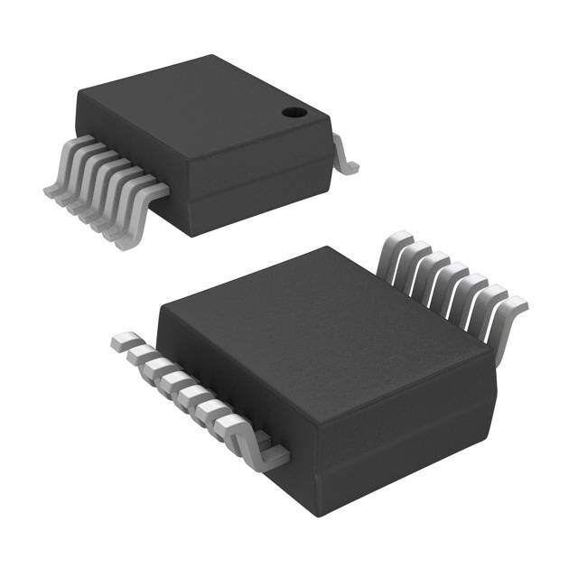
| 产品图片 |
|
| rohs | 符合RoHS无铅 / 符合限制有害物质指令(RoHS)规范要求 |
| 产品系列 | 逻辑集成电路,单稳态多谐振荡器,Texas Instruments SN74AHC123ADGVR74AHC |
| 数据手册 | |
| 产品型号 | SN74AHC123ADGVR |
| 产品目录页面 | |
| 产品种类 | 单稳态多谐振荡器 |
| 传播延迟 | 7.5ns |
| 传播延迟时间 | 24.1 ns, 14 ns |
| 低电平输出电流 | 8 mA |
| 供应商器件封装 | 16-TVSOP |
| 其它名称 | 296-4526-6 |
| 包装 | Digi-Reel® |
| 单位重量 | 42 mg |
| 商标 | Texas Instruments |
| 安装类型 | 表面贴装 |
| 安装风格 | SMD/SMT |
| 封装 | Reel |
| 封装/外壳 | 16-TFSOP (0.173",4.40mm 宽) |
| 封装/箱体 | TVSOP-16 |
| 工作温度 | -40°C ~ 85°C |
| 工作电源电压 | 2.5 V, 3.3 V, 5 V |
| 工厂包装数量 | 2000 |
| 施密特触发器输入 | 是 |
| 最大工作温度 | + 85 C |
| 最小工作温度 | - 40 C |
| 标准包装 | 1 |
| 每芯片元件 | 2 |
| 独立电路 | 2 |
| 电压-电源 | 2 V ~ 5.5 V |
| 电流-输出高,低 | 8mA,8mA |
| 电源电压-最大 | 5.5 V |
| 电源电压-最小 | 2 V |
| 系列 | SN74AHC123A |
| 逻辑类型 | 单稳态 |
| 逻辑系列 | AHC |
| 高电平输出电流 | - 8 mA |


PDF Datasheet 数据手册内容提取
(cid:1)(cid:2)(cid:3)(cid:4)(cid:5)(cid:6)(cid:7)(cid:8)(cid:9)(cid:10)(cid:5)(cid:11) (cid:1)(cid:2)(cid:12)(cid:4)(cid:5)(cid:6)(cid:7)(cid:8)(cid:9)(cid:10)(cid:5) (cid:13)(cid:14)(cid:5)(cid:15) (cid:16)(cid:17)(cid:18)(cid:16)(cid:19)(cid:20)(cid:20)(cid:17)(cid:16)(cid:5)(cid:21)(cid:15)(cid:17) (cid:22)(cid:23)(cid:2)(cid:23)(cid:1)(cid:18)(cid:5)(cid:21)(cid:15)(cid:17) (cid:22)(cid:14)(cid:15)(cid:18)(cid:19)(cid:24)(cid:19)(cid:21)(cid:16)(cid:5)(cid:18)(cid:23)(cid:16)(cid:1) SCLS352H − JULY 1997 − REVISED OCTOBER 2005 (cid:1) Operating Range 2-V to 5.5-V V SN54AHC123A...J OR W PACKAGE CC (cid:1) SN74AHC123A...D, DB, DGV, N, OR PW PACKAGE Schmitt-Trigger Circuitry On A, B, and CLR (TOP VIEW) Inputs for Slow Input Transition Rates (cid:1) Edge Triggered From Active-High or 1A 1 16 VCC Active-Low Gated Logic Inputs 1B 2 15 1Rext/Cext (cid:1) Retriggerable for Very Long Output Pulses 1CLR 3 14 1Cext (cid:1) 1Q 4 13 1Q Overriding Clear Terminates Output Pulse (cid:1) 2Q 5 12 2Q Glitch-Free Power-Up Reset On Outputs (cid:1) 2Cext 6 11 2CLR Latch-Up Performance Exceeds 100 mA Per 2R /C 7 10 2B ext ext JESD 78, Class II GND 8 9 2A (cid:1) ESD Protection Exceeds JESD 22 − 2000-V Human-Body Model (A114-A) SN54AHC123A...FK PACKAGE − 200-V Machine Model (A115-A) (TOP VIEW) − 1000-V Charged-Device Model (C101) xt e C description/ordering information / xt C e B A C CR The ’AHC123A devices are dual retriggerable 1 1 N V 1 monostable multivibrators designed for 2-V to 3 2 1 20 19 5.5-V VCC operation. 1CLR 4 18 1Cext 1Q 5 17 1Q These edge-triggered multivibrators feature NC 6 16 NC output pulse-duration control by three methods. In 2Q 7 15 2Q the first method, the A input is low, and the B input goes high. In the second method, the B input is 2Cext 8 14 2CLR 9 10 1112 13 high, and the A input goes low. In the third method, the A input is low, the B input is high, and the clear xtD C AB eN N 22 (CLR) input goes high. C G / xt e R 2 NC − No internal connection ORDERING INFORMATION ORDERABLE TOP-SIDE TA PACKAGE† PART NUMBER MARKING PDIP − N Tube SN74AHC123AN SN74AHC123AN Tube SN74AHC123AD SSOOIICC −− DD AAHHCC112233AA Tape and reel SN74AHC123ADR −−4400°°CC ttoo 8855°°CC SSOP − DB Tape and reel SN74AHC123ADBR HA123A TSSOP − PW Tape and reel SN74AHC123APWR HA123A TVSOP − DGV Tape and reel SN74AHC123ADGVR HA123A CDIP − J Tube SNJ54AHC123AJ SNJ54AHC123AJ −−5555°CC ttoo 112255°CC CFP − W Tube SNJ54AHC123AW SNJ54AHC123AW LCCC − FK Tube SNJ54AHC123AFK SNJ54AHC123AFK †Package drawings, standard packing quantities, thermal data, symbolization, and PCB design guidelines are available at www.ti.com/sc/package. Please be aware that an important notice concerning availability, standard warranty, and use in critical applications of TexasInstruments semiconductor products and disclaimers thereto appears at the end of this data sheet. (cid:25)(cid:16)(cid:23)(cid:13)(cid:14)(cid:7)(cid:18)(cid:19)(cid:23)(cid:2) (cid:13)(cid:5)(cid:18)(cid:5) (cid:26)(cid:27)(cid:28)(cid:29)(cid:30)(cid:31)!"(cid:26)(cid:29)(cid:27) (cid:26)# $%(cid:30)(cid:30)&(cid:27)" !# (cid:29)(cid:28) ’%()(cid:26)$!"(cid:26)(cid:29)(cid:27) *!"&+ Copyright 2005, Texas Instruments Incorporated (cid:25)(cid:30)(cid:29)*%$"# $(cid:29)(cid:27)(cid:28)(cid:29)(cid:30)(cid:31) "(cid:29) #’&$(cid:26)(cid:28)(cid:26)$!"(cid:26)(cid:29)(cid:27)# ’&(cid:30) ",& "&(cid:30)(cid:31)# (cid:29)(cid:28) (cid:18)&-!# (cid:19)(cid:27)#"(cid:30)%(cid:31)&(cid:27)"# (cid:23)(cid:27) ’(cid:30)(cid:29)*%$"# $(cid:29)(cid:31)’)(cid:26)!(cid:27)" "(cid:29) (cid:22)(cid:19)(cid:15)1(cid:25)(cid:16)21(cid:10)3(cid:3)(cid:10)(cid:3)(cid:11) !)) ’!(cid:30)!(cid:31)&"&(cid:30)# !(cid:30)& "&#"&* #"!(cid:27)*!(cid:30)* .!(cid:30)(cid:30)!(cid:27)"/+ (cid:25)(cid:30)(cid:29)*%$"(cid:26)(cid:29)(cid:27) ’(cid:30)(cid:29)$&##(cid:26)(cid:27)0 *(cid:29)&# (cid:27)(cid:29)" (cid:27)&$&##!(cid:30)(cid:26))/ (cid:26)(cid:27)$)%*& %(cid:27))&## (cid:29)",&(cid:30).(cid:26)#& (cid:27)(cid:29)"&*+ (cid:23)(cid:27) !)) (cid:29)",&(cid:30) ’(cid:30)(cid:29)*%$"#(cid:11) ’(cid:30)(cid:29)*%$"(cid:26)(cid:29)(cid:27) "&#"(cid:26)(cid:27)0 (cid:29)(cid:28) !)) ’!(cid:30)!(cid:31)&"&(cid:30)#+ ’(cid:30)(cid:29)$&##(cid:26)(cid:27)0 *(cid:29)&# (cid:27)(cid:29)" (cid:27)&$&##!(cid:30)(cid:26))/ (cid:26)(cid:27)$)%*& "&#"(cid:26)(cid:27)0 (cid:29)(cid:28) !)) ’!(cid:30)!(cid:31)&"&(cid:30)#+ POST OFFICE BOX 655303 • DALLAS, TEXAS 75265 1
(cid:1)(cid:2)(cid:3)(cid:4)(cid:5)(cid:6)(cid:7)(cid:8)(cid:9)(cid:10)(cid:5)(cid:11) (cid:1)(cid:2)(cid:12)(cid:4)(cid:5)(cid:6)(cid:7)(cid:8)(cid:9)(cid:10)(cid:5) (cid:13)(cid:14)(cid:5)(cid:15) (cid:16)(cid:17)(cid:18)(cid:16)(cid:19)(cid:20)(cid:20)(cid:17)(cid:16)(cid:5)(cid:21)(cid:15)(cid:17) (cid:22)(cid:23)(cid:2)(cid:23)(cid:1)(cid:18)(cid:5)(cid:21)(cid:15)(cid:17) (cid:22)(cid:14)(cid:15)(cid:18)(cid:19)(cid:24)(cid:19)(cid:21)(cid:16)(cid:5)(cid:18)(cid:23)(cid:16)(cid:1) SCLS352H − JULY 1997 − REVISED OCTOBER 2005 description/ordering information (continued) The output pulse duration is programmed by selecting external resistance and capacitance values. The external timing capacitor must be connected between C and R /C (positive) and an external resistor connected ext ext ext between R /C and V . To obtain variable pulse durations, connect an external variable resistance between ext ext CC R /C and V . The output pulse duration also can be reduced by taking CLR low. ext ext CC Pulse triggering occurs at a particular voltage level and is not directly related to the transition time of the input pulse. The A, B, and CLR inputs have Schmitt triggers with sufficient hysteresis to handle slow input transition rates with jitter-free triggering at the outputs. Once triggered, the basic pulse duration can be extended by retriggering the gated low-level-active (A) or high-level-active (B) input. Pulse duration can be reduced by taking CLR low. CLR input can be used to override A or B inputs. The input/output timing diagram illustrates pulse control by retriggering the inputs and early clearing. The variance in output pulse duration from device to device typically is less than ±0.5% for given external timing components. An example of this distribution for the ’AHC123A is shown in Figure 10. Variations in output pulse duration versus supply voltage and temperature are shown in Figure 6. During power up, Q outputs are in the low state, and Q outputs are in the high state. The outputs are glitch free, without applying a reset pulse. For additional application information on multivibrators, see the application report Designing With the SN74AHC123A and SN74AHCT123A, literature number SCLA014. FUNCTION TABLE (each multivibrator) INPUTS OUTPUTS CLR A B Q Q L X X L H X H X L† H† X X L L† H† H L ↑ H (cid:1) H ↑ L H †These outputs are based on the assumption that the indicated steady-state conditions at the A and B inputs have been set up long enough to complete any pulse started before the setup. 2 POST OFFICE BOX 655303 • DALLAS, TEXAS 75265
(cid:1)(cid:2)(cid:3)(cid:4)(cid:5)(cid:6)(cid:7)(cid:8)(cid:9)(cid:10)(cid:5)(cid:11) (cid:1)(cid:2)(cid:12)(cid:4)(cid:5)(cid:6)(cid:7)(cid:8)(cid:9)(cid:10)(cid:5) (cid:13)(cid:14)(cid:5)(cid:15) (cid:16)(cid:17)(cid:18)(cid:16)(cid:19)(cid:20)(cid:20)(cid:17)(cid:16)(cid:5)(cid:21)(cid:15)(cid:17) (cid:22)(cid:23)(cid:2)(cid:23)(cid:1)(cid:18)(cid:5)(cid:21)(cid:15)(cid:17) (cid:22)(cid:14)(cid:15)(cid:18)(cid:19)(cid:24)(cid:19)(cid:21)(cid:16)(cid:5)(cid:18)(cid:23)(cid:16)(cid:1) SCLS352H − JULY 1997 − REVISED OCTOBER 2005 logic diagram, each multivibrator (positive logic) Rext/Cext A Cext B Q CLR R Q input/output timing diagram trr A B CLR Rext/Cext Q Q tw tw tw + trr POST OFFICE BOX 655303 • DALLAS, TEXAS 75265 3
(cid:1)(cid:2)(cid:3)(cid:4)(cid:5)(cid:6)(cid:7)(cid:8)(cid:9)(cid:10)(cid:5)(cid:11) (cid:1)(cid:2)(cid:12)(cid:4)(cid:5)(cid:6)(cid:7)(cid:8)(cid:9)(cid:10)(cid:5) (cid:13)(cid:14)(cid:5)(cid:15) (cid:16)(cid:17)(cid:18)(cid:16)(cid:19)(cid:20)(cid:20)(cid:17)(cid:16)(cid:5)(cid:21)(cid:15)(cid:17) (cid:22)(cid:23)(cid:2)(cid:23)(cid:1)(cid:18)(cid:5)(cid:21)(cid:15)(cid:17) (cid:22)(cid:14)(cid:15)(cid:18)(cid:19)(cid:24)(cid:19)(cid:21)(cid:16)(cid:5)(cid:18)(cid:23)(cid:16)(cid:1) SCLS352H − JULY 1997 − REVISED OCTOBER 2005 absolute maximum ratings over operating free-air temperature (unless otherwise noted)† Supply voltage range, VCC (see Note 1) . . . . . . . . . . . . . . . . . . . . . . . . . . . . . . . . . . . . . . . . . . . . . . −0.5 V to 7 V Input voltage range, VI (see Note 2) . . . . . . . . . . . . . . . . . . . . . . . . . . . . . . . . . . . . . . . . . . . . . . . . . . −0.5 V to 7 V Output voltage range in high or low state, V (see Note 1) . . . . . . . . . . . . . . . . . . . . . . . −0.5 V to V + 0.5 V O CC Output voltage range in power-off state, V (see Note 1) . . . . . . . . . . . . . . . . . . . . . . . . . . . . . . . . −0.5 V to 7 V O Input clamp current, IIK (VI < 0) . . . . . . . . . . . . . . . . . . . . . . . . . . . . . . . . . . . . . . . . . . . . . . . . . . . . . . . . . . . −20 mA Output clamp current, IOK (VO < 0 or VO > VCC) . . . . . . . . . . . . . . . . . . . . . . . . . . . . . . . . . . . . . . . . . . . . ±20 mA Continuous output current, IO (VO = 0 to VCC) . . . . . . . . . . . . . . . . . . . . . . . . . . . . . . . . . . . . . . . . . . . . . . ±25 mA Continuous current through V or GND . . . . . . . . . . . . . . . . . . . . . . . . . . . . . . . . . . . . . . . . . . . . . . . . . . . ±50 mA CC Package thermal impedance, θ (see Note 3): D package . . . . . . . . . . . . . . . . . . . . . . . . . . . . . . . . . . . 73°C/W JA DB package . . . . . . . . . . . . . . . . . . . . . . . . . . . . . . . . . 82°C/W DGV package . . . . . . . . . . . . . . . . . . . . . . . . . . . . . . . 120°C/W N package . . . . . . . . . . . . . . . . . . . . . . . . . . . . . . . . . . . 67°C/W PW package . . . . . . . . . . . . . . . . . . . . . . . . . . . . . . . . 108°C/W Storage temperature range, T . . . . . . . . . . . . . . . . . . . . . . . . . . . . . . . . . . . . . . . . . . . . . . . . . . . −65°C to 150°C stg †Stresses beyond those listed under “absolute maximum ratings” may cause permanent damage to the device. These are stress ratings only, and functional operation of the device at these or any other conditions beyond those indicated under “recommended operating conditions” is not implied. Exposure to absolute-maximum-rated conditions for extended periods may affect device reliability. NOTES: 1. Voltage values are with respect to the network ground terminal. 2. The input and output voltage ratings may be exceeded if the input and output current ratings are observed. 3. The package thermal impedance is calculated in accordance with JESD 51-7. recommended operating conditions (see Note 4) SN54AHC123A SN74AHC123A UUNNIITT MIN MAX MIN MAX VCC Supply voltage 2 5.5 2 5.5 V VCC = 2 V 1.5 1.5 VVIIHH HHiigghh--lleevveell iinnppuutt vvoollttaaggee VCC = 3 V 2.1 2.1 VV VCC = 5.5 V 3.85 3.85 VCC = 2 V 0.5 0.5 VVIILL LLooww--lleevveell iinnppuutt vvoollttaaggee VCC = 3 V 0.9 0.9 VV VCC = 5.5 V 1.65 1.65 VI Input voltage 0 5.5 0 5.5 V VO Output voltage 0 VCC 0 VCC V VCC = 2 V −50 −50 (cid:1)A IIOOHH HHiigghh--lleevveell oouuttppuutt ccuurrrreenntt VCC = 3.3 V ± 0.3 V −4 −4 mmAA VCC = 5 V ± 0.5 V −8 −8 VCC = 2 V 50 50 (cid:1)A IIOOLL LLooww--lleevveell oouuttppuutt ccuurrrreenntt VCC = 3.3 V ± 0.3 V 4 4 mmAA VCC = 5 V ± 0.5 V 8 8 VCC = 2 V 5k 5k RReexxtt EExxtteerrnnaall ttiimmiinngg rreessiissttaannccee ΩΩ VCC > 3 V 1k 1k ∆t/∆VCC Power-up ramp rate 1 1 ms/V TA Operating free-air temperature −55 125 −40 85 °C NOTE 4: Unused Rext/Cext terminals should be left unconnected. All remaining unused inputs of the device must be held at VCC or GND to ensure proper device operation. Refer to the TI application report, Implications of Slow or Floating CMOS Inputs, literature number SCBA004. 4 POST OFFICE BOX 655303 • DALLAS, TEXAS 75265
(cid:1)(cid:2)(cid:3)(cid:4)(cid:5)(cid:6)(cid:7)(cid:8)(cid:9)(cid:10)(cid:5)(cid:11) (cid:1)(cid:2)(cid:12)(cid:4)(cid:5)(cid:6)(cid:7)(cid:8)(cid:9)(cid:10)(cid:5) (cid:13)(cid:14)(cid:5)(cid:15) (cid:16)(cid:17)(cid:18)(cid:16)(cid:19)(cid:20)(cid:20)(cid:17)(cid:16)(cid:5)(cid:21)(cid:15)(cid:17) (cid:22)(cid:23)(cid:2)(cid:23)(cid:1)(cid:18)(cid:5)(cid:21)(cid:15)(cid:17) (cid:22)(cid:14)(cid:15)(cid:18)(cid:19)(cid:24)(cid:19)(cid:21)(cid:16)(cid:5)(cid:18)(cid:23)(cid:16)(cid:1) SCLS352H − JULY 1997 − REVISED OCTOBER 2005 electrical characteristics over recommended operating free-air temperature range (unless otherwise noted) TA = 25°C SN54AHC123A SN74AHC123A PPAARRAAMMEETTEERR TTEESSTT CCOONNDDIITTIIOONNSS VVCCCC UUNNIITT MIN TYP MAX MIN MAX MIN MAX 2 V 1.9 2 1.9 1.9 IIOOHH == −−5500 (cid:1)(cid:1)AA 3 V 2.9 3 2.9 2.9 VVOOHH 4.5 V 4.4 4.5 4.4 4.4 VV IOH = −4 mA 3 V 2.58 2.48 2.48 IOH = −8 mA 4.5 V 3.94 3.8 3.8 2 V 0.1 0.1 0.1 IIOOLL == 5500 (cid:1)(cid:1)AA 3 V 0.1 0.1 0.1 VVOOLL 4.5 V 0.1 0.1 0.1 VV IOL = 4 mA 3 V 0.36 0.5 0.44 IOL = 8 mA 4.5 V 0.36 0.5 0.44 Rext/Cext† VI = VCC or GND 5.5 V ±0.25 ±2.5 ±2.5 IIII (cid:1)AA A, B, and CLR VI = VCC or GND 0 V to 5.5 V ±0.1 ±1* ±1 ICC Quiescent VI = VCC or GND, IO = 0 5.5 V 4 40 40 (cid:1)A 3 V 160 250 280 280 IICCCC AA((ppcceettiirrvv cceeii rrssccttuuaaiittttee)) VVRRIIee ==xxtt //VVCCCCeeCCxxtt oo==rr 00GG..55NN DDVVCC,, CC 4.5 V 280 500 650 650 (cid:1)(cid:1)AA 5.5 V 360 750 975 975 Ci VI = VCC or GND 5 V 1.9 10 10 pF * On products compliant to MIL-PRF-38535, this parameter is not production tested at VCC = 0 V. †This test is performed with the terminal in the off-state condition. timing requirements over recommended operating free-air temperature range, V = 3.3 V ± 0.3 V CC (unless otherwise noted) (see Figure 1) TA = 25°C SN54AHC123A SN74AHC123A TTEESSTT CCOONNDDIITTIIOONNSS UUNNIITT MIN TYP MAX MIN MAX MIN MAX PPuullssee CLR 5 5 5 ttww duration A or B trigger 5 5 5 nnss Rext = 1 kΩ, Cext = 100 pF ‡ 76 ‡ ‡ ns ttrrrr PPuullssee rreettrriiggggeerr ttiimmee Rext = 1 kΩ, Cext = 0.01 (cid:1)F ‡ 1.8 ‡ ‡ (cid:1)s ‡See retriggering data in the application information section. timing requirements over recommended operating free-air temperature range, V = 5 V ± 0.5 V CC (unless otherwise noted) (see Figure 1) TA = 25°C SN54AHC123A SN74AHC123A TTEESSTT CCOONNDDIITTIIOONNSS UUNNIITT MIN TYP MAX MIN MAX MIN MAX PPuullssee CLR 5 5 5 ttww duration A or B trigger 5 5 5 nnss Rext = 1 kΩ, Cext = 100 pF ‡ 59 ‡ ‡ ns ttrrrr PPuullssee rreettrriiggggeerr ttiimmee Rext = 1 kΩ, Cext = 0.01 (cid:1)F ‡ 1.5 ‡ ‡ (cid:1)s ‡See retriggering data in the application information section. POST OFFICE BOX 655303 • DALLAS, TEXAS 75265 5
(cid:1)(cid:2)(cid:3)(cid:4)(cid:5)(cid:6)(cid:7)(cid:8)(cid:9)(cid:10)(cid:5)(cid:11) (cid:1)(cid:2)(cid:12)(cid:4)(cid:5)(cid:6)(cid:7)(cid:8)(cid:9)(cid:10)(cid:5) (cid:13)(cid:14)(cid:5)(cid:15) (cid:16)(cid:17)(cid:18)(cid:16)(cid:19)(cid:20)(cid:20)(cid:17)(cid:16)(cid:5)(cid:21)(cid:15)(cid:17) (cid:22)(cid:23)(cid:2)(cid:23)(cid:1)(cid:18)(cid:5)(cid:21)(cid:15)(cid:17) (cid:22)(cid:14)(cid:15)(cid:18)(cid:19)(cid:24)(cid:19)(cid:21)(cid:16)(cid:5)(cid:18)(cid:23)(cid:16)(cid:1) SCLS352H − JULY 1997 − REVISED OCTOBER 2005 switching characteristics over recommended operating free-air temperature range, VCC = 3.3 V± 0.3 V (unless otherwise noted) (see Figure 1) FFRROOMM TTOO TTEESSTT TA = 25°C SN54AHC123A SN74AHC123A PPAARRAAMMEETTEERR UUNNIITT (INPUT) (OUTPUT) CONDITIONS MIN TYP MAX MIN MAX MIN MAX tPLH 9.5* 20.6* 1* 24* 1 24 AA oorr BB QQ oorr QQ CCLL == 1155 ppFF nnss tPHL 10.2* 20.6* 1* 24* 1 24 tPLH 7.5* 15.8* 1* 18.5* 1 18.5 CCLLRR QQ oorr QQ CCLL == 1155 ppFF nnss tPHL 9.3* 15.8* 1* 18.5* 1 18.5 tPLH 10* 22.4* 1* 26* 1 26 CCLLRR ttrriiggggeerr QQ oorr QQ CCLL == 1155 ppFF nnss tPHL 10.6* 22.4* 1* 26* 1 26 tPLH 10.5 24.1 1 27.5 1 27.5 AA oorr BB QQ oorr QQ CCLL == 5500 ppFF nnss tPHL 11.8 24.1 1 27.5 1 27.5 tPLH 8.9 19.3 1 22 1 22 CCLLRR QQ oorr QQ CCLL == 5500 ppFF nnss tPHL 10.5 19.3 1 22 1 22 tPLH 11 25.9 1 29.5 1 29.5 CCLLRR ttrriiggggeerr QQ oorr QQ CCLL == 5500 ppFF nnss tPHL 12.3 25.9 1 29.5 1 29.5 CL = 50 pF, Cext = 28 pF, 182 240 300 300 ns Rext = 2 kΩ CL = 50 pF, tw† Q or Q Cext = 0.01 µF, 90 100 110 90 110 90 110 (cid:1)s Rext = 10 kΩ CL = 50 pF, Cext = 0.1 µF, 0.9 1 1.1 0.9 1.1 0.9 1.1 ms Rext = 10 kΩ ∆tw‡ ±1 % * On products compliant to MIL-PRF-38535, this parameter is not production tested. †tw = Pulse duration at Q and Q outputs ‡∆tw = Output pulse-duration variation (Q and Q) between circuits in same package 6 POST OFFICE BOX 655303 • DALLAS, TEXAS 75265
(cid:1)(cid:2)(cid:3)(cid:4)(cid:5)(cid:6)(cid:7)(cid:8)(cid:9)(cid:10)(cid:5)(cid:11) (cid:1)(cid:2)(cid:12)(cid:4)(cid:5)(cid:6)(cid:7)(cid:8)(cid:9)(cid:10)(cid:5) (cid:13)(cid:14)(cid:5)(cid:15) (cid:16)(cid:17)(cid:18)(cid:16)(cid:19)(cid:20)(cid:20)(cid:17)(cid:16)(cid:5)(cid:21)(cid:15)(cid:17) (cid:22)(cid:23)(cid:2)(cid:23)(cid:1)(cid:18)(cid:5)(cid:21)(cid:15)(cid:17) (cid:22)(cid:14)(cid:15)(cid:18)(cid:19)(cid:24)(cid:19)(cid:21)(cid:16)(cid:5)(cid:18)(cid:23)(cid:16)(cid:1) SCLS352H − JULY 1997 − REVISED OCTOBER 2005 switching characteristics over recommended operating free-air temperature range, VCC = 5 V± 0.5 V (unless otherwise noted) (see Figure 1) FFRROOMM TTOO TTEESSTT TA = 25°C SN54AHC123A SN74AHC123A PPAARRAAMMEETTEERR UUNNIITT (NPUT) (OUTPUT) CONDITIONS MIN TYP MAX MIN MAX MIN MAX tPLH 6.5* 12* 1* 14* 1 14 AA oorr BB QQ oorr QQ CCLL == 1155 ppFF nnss tPHL 7.1* 12* 1* 14* 1 14 tPLH 5.3* 9.4* 1* 11* 1 11 CCLLRR QQ oorr QQ CCLL == 1155 ppFF nnss tPHL 6.5* 9.4* 1* 11* 1 11 tPLH 6.9* 12.9* 1* 15* 1 15 CCLLRR ttrriiggggeerr QQ oorr QQ CCLL == 1155 ppFF nnss tPHL 7.4* 12.9* 1* 15* 1 15 tPLH 7.3 14 1 16 1 16 AA oorr BB QQ oorr QQ CCLL == 5500 ppFF nnss tPHL 8.3 14 1 16 1 16 tPLH 6.3 11.4 1 13 1 13 CCLLRR QQ oorr QQ CCLL == 5500 ppFF nnss tPHL 7.4 11.4 1 13 1 13 tPLH 7.6 14.9 1 17 1 17 CCLLRR ttrriiggggeerr QQ oorr QQ CCLL == 5500 ppFF nnss tPHL 8.7 14.9 1 17 1 17 CL = 50 pF, Cext = 28 pF, 167 200 240 240 ns Rext = 2 kΩ CL = 50 pF, tw† Q or Q Cext = 0.01 µF, 90 100 110 90 110 90 110 (cid:1)s Rext = 10 kΩ CL = 50 pF, Cext = 0.1 µF, 0.9 1 1.1 0.9 1.1 0.9 1.1 ms Rext = 10 kΩ ∆tw‡ ±1 % * On products compliant to MIL-PRF-38535, this parameter is not production tested. †tw = Pulse duration at Q and Q outputs ‡∆tw = Output pulse-duration variation (Q and Q) between circuits in same package operating characteristics, VCC = 5 V, TA = 25°C PARAMETER TEST CONDITIONS TYP UNIT Cpd Power dissipation capacitance No load 29 pF POST OFFICE BOX 655303 • DALLAS, TEXAS 75265 7
(cid:1)(cid:2)(cid:3)(cid:4)(cid:5)(cid:6)(cid:7)(cid:8)(cid:9)(cid:10)(cid:5)(cid:11) (cid:1)(cid:2)(cid:12)(cid:4)(cid:5)(cid:6)(cid:7)(cid:8)(cid:9)(cid:10)(cid:5) (cid:13)(cid:14)(cid:5)(cid:15) (cid:16)(cid:17)(cid:18)(cid:16)(cid:19)(cid:20)(cid:20)(cid:17)(cid:16)(cid:5)(cid:21)(cid:15)(cid:17) (cid:22)(cid:23)(cid:2)(cid:23)(cid:1)(cid:18)(cid:5)(cid:21)(cid:15)(cid:17) (cid:22)(cid:14)(cid:15)(cid:18)(cid:19)(cid:24)(cid:19)(cid:21)(cid:16)(cid:5)(cid:18)(cid:23)(cid:16)(cid:1) SCLS352H − JULY 1997 − REVISED OCTOBER 2005 PARAMETER MEASUREMENT INFORMATION From Output Test Under Test Point tw CL VCC (see Note A) Inputs or Outputs 50% VCC 50% VCC 0 V LOAD CIRCUIT VOLTAGE WAVEFORMS PULSE DURATION VCC Input A (see Note B) 50% VCC 0 V Input CLR VCC Input B VCC (see Note B) 50% VCC 50% VCC 0 V (see Note B) 50% VCC 0 V tPLH tPHL tPLH VOH In-Phase VOH InO-Puhtapsuet 50% VCC 50% VCC Output 50% VCC VOL VOL tPHL tPHL tPLH VOH VOH Out-of-Phase 50% VCC Out-of-Phase 50% VCC 50% VCC Output Output VOL VOL VOLTAGE WAVEFORMS VOLTAGE WAVEFORMS DELAY TIMES DELAY TIMES NOTES: A. CL includes probe and jig capacitance. B. All input pulses are supplied by generators having the following characteristics: ZO = 50 Ω, tr (cid:1)3 ns, tf (cid:1) 3 ns. C. The outputs are measured one at a time, with one input transition per measurement. Figure 1. Load Circuit and Voltage Waveforms 8 POST OFFICE BOX 655303 • DALLAS, TEXAS 75265
(cid:1)(cid:2)(cid:3)(cid:4)(cid:5)(cid:6)(cid:7)(cid:8)(cid:9)(cid:10)(cid:5)(cid:11) (cid:1)(cid:2)(cid:12)(cid:4)(cid:5)(cid:6)(cid:7)(cid:8)(cid:9)(cid:10)(cid:5) (cid:13)(cid:14)(cid:5)(cid:15) (cid:16)(cid:17)(cid:18)(cid:16)(cid:19)(cid:20)(cid:20)(cid:17)(cid:16)(cid:5)(cid:21)(cid:15)(cid:17) (cid:22)(cid:23)(cid:2)(cid:23)(cid:1)(cid:18)(cid:5)(cid:21)(cid:15)(cid:17) (cid:22)(cid:14)(cid:15)(cid:18)(cid:19)(cid:24)(cid:19)(cid:21)(cid:16)(cid:5)(cid:18)(cid:23)(cid:16)(cid:1) SCLS352H − JULY 1997 − REVISED OCTOBER 2005 APPLICATION INFORMATION caution in use To prevent malfunctions due to noise, connect a high-frequency capacitor between V and GND, and keep CC the wiring between the external components and C and R /C terminals as short as possible. ext ext ext power-down considerations Large values of C can cause problems when powering down the ’AHC123A devices because of the amount ext of energy stored in the capacitor. When a system containing this device is powered down, the capacitor can discharge from V through the protection diodes at pin 2 or pin 14. Current through the input protection diodes CC must be limited to 30 mA; therefore, the turn-off time of the V power supply must not be faster than CC t = V × C /30 mA. For example, if V = 5 V and C = 15 pF, the V supply must turn off no faster than CC ext CC ext CC t = (5 V) × (15 pF)/30 mA = 2.5 ns. Usually, this is not a problem because power supplies are heavily filtered and cannot discharge at this rate. When a more rapid decrease of V to zero occurs, the ’AHC123A devices CC can sustain damage. To avoid this possibility, use external clamping diodes. output pulse duration The output pulse duration, t , is determined primarily by the values of the external capacitance (C ) and timing w T resistance (R ). The timing components are connected as shown in Figure 2. T VCC RT CT To Rext/Cext To Cext Terminal Terminal Figure 2. Timing-Component Connections The pulse duration is given by: tw(cid:1)K(cid:2)RT(cid:2)CT (1) if C is ≥1000 pF, K = 1.0 or T if C is <1000 pF, K can be determined from Figure 9 T where: t = pulse duration in ns w R = external timing resistance in kΩ T C = external capacitance in pF T K = multiplier factor Equation 1 and Figure 3 can be used to determine values for pulse duration, external resistance, and external capacitance. POST OFFICE BOX 655303 • DALLAS, TEXAS 75265 9
(cid:1)(cid:2)(cid:3)(cid:4)(cid:5)(cid:6)(cid:7)(cid:8)(cid:9)(cid:10)(cid:5)(cid:11) (cid:1)(cid:2)(cid:12)(cid:4)(cid:5)(cid:6)(cid:7)(cid:8)(cid:9)(cid:10)(cid:5) (cid:13)(cid:14)(cid:5)(cid:15) (cid:16)(cid:17)(cid:18)(cid:16)(cid:19)(cid:20)(cid:20)(cid:17)(cid:16)(cid:5)(cid:21)(cid:15)(cid:17) (cid:22)(cid:23)(cid:2)(cid:23)(cid:1)(cid:18)(cid:5)(cid:21)(cid:15)(cid:17) (cid:22)(cid:14)(cid:15)(cid:18)(cid:19)(cid:24)(cid:19)(cid:21)(cid:16)(cid:5)(cid:18)(cid:23)(cid:16)(cid:1) SCLS352H − JULY 1997 − REVISED OCTOBER 2005 APPLICATION INFORMATION retriggering data The minimum input retriggering time (t ) is the minimum time required after the initial signal before retriggering MIR the input. After t , the device retriggers the output. Experimentally, it also can be shown that to retrigger the MIR output pulse, the two adjacent input signals should be t apart, where t = 0.30 × t . The retrigger pulse MIR MIR w duration is calculated as shown in Figure 3. tMIR Input tRT = tw + tPLH = (K × RT × CT) + tPLH tPLH tRT Where: tw tMIR = Minimum Input Retriggering Time tPLH= Propagation Delay Output tRT = Retrigger Time tw = Output Pulse Duration Before Retriggering Figure 3. Retrigger Pulse Duration The minimum value from the end of the input pulse to the beginning of the retriggered output should be approximately 15 ns to ensure a retriggered output (see Figure 4). Input tMRT Output tMRT= Minimum Time Between the End of the Second Input Pulse and the Beginning of the Retriggered Output tMRT= 15 ns Figure 4. Input/Output Requirements 10 POST OFFICE BOX 655303 • DALLAS, TEXAS 75265
(cid:1)(cid:2)(cid:3)(cid:4)(cid:5)(cid:6)(cid:7)(cid:8)(cid:9)(cid:10)(cid:5)(cid:11) (cid:1)(cid:2)(cid:12)(cid:4)(cid:5)(cid:6)(cid:7)(cid:8)(cid:9)(cid:10)(cid:5) (cid:13)(cid:14)(cid:5)(cid:15) (cid:16)(cid:17)(cid:18)(cid:16)(cid:19)(cid:20)(cid:20)(cid:17)(cid:16)(cid:5)(cid:21)(cid:15)(cid:17) (cid:22)(cid:23)(cid:2)(cid:23)(cid:1)(cid:18)(cid:5)(cid:21)(cid:15)(cid:17) (cid:22)(cid:14)(cid:15)(cid:18)(cid:19)(cid:24)(cid:19)(cid:21)(cid:16)(cid:5)(cid:18)(cid:23)(cid:16)(cid:1) SCLS352H − JULY 1997 − REVISED OCTOBER 2005 APPLICATION INFORMATION† 1.00E+09 VCC = 5 V TA = 25°C 1.00E+08 RT = 200k Ω 1.00E+07 s − n 1.00E+06 RT = 150k Ω n o urati 1.00E+05 RT = 80k Ω RT = 10k Ω D e s Pul 1.00E+04 ut p ut O 1.00E+03 RT = 5k Ω − w t 1.00E+02 RT = 1k Ω 1.00E+01 1.00E+00 1 10 102 103 104 105 106 107 CT − External Timing Capacitance − pF Figure 5. Output Pulse Duration vs External Timing Capacitance 14% tw = 866 ns at: 12% VCC = 5 V n RT = 10 kΩ VCC = 2.5 V uratio 10% TCAT == 2550° pCF VVCCCC == 33. 5V V D 8% e VCC = 4 V s Pul 6% VCC = 5 V put 4% VCC = 6 V Out VCC = 7 V n 2% n i o 0% ati ari −2% V −4% −6% −60 −40 −20 0 20 40 60 80 100 120 140 160 180 Temperature − °C Figure 6. Variations in Output Pulse Duration vs Temperature †Operation of the device at these or any other conditions beyond those indicated under “recommended operating conditions” is not implied. POST OFFICE BOX 655303 • DALLAS, TEXAS 75265 11
(cid:1)(cid:2)(cid:3)(cid:4)(cid:5)(cid:6)(cid:7)(cid:8)(cid:9)(cid:10)(cid:5)(cid:11) (cid:1)(cid:2)(cid:12)(cid:4)(cid:5)(cid:6)(cid:7)(cid:8)(cid:9)(cid:10)(cid:5) (cid:13)(cid:14)(cid:5)(cid:15) (cid:16)(cid:17)(cid:18)(cid:16)(cid:19)(cid:20)(cid:20)(cid:17)(cid:16)(cid:5)(cid:21)(cid:15)(cid:17) (cid:22)(cid:23)(cid:2)(cid:23)(cid:1)(cid:18)(cid:5)(cid:21)(cid:15)(cid:17) (cid:22)(cid:14)(cid:15)(cid:18)(cid:19)(cid:24)(cid:19)(cid:21)(cid:16)(cid:5)(cid:18)(cid:23)(cid:16)(cid:1) SCLS352H − JULY 1997 − REVISED OCTOBER 2005 APPLICATION INFORMATION† MINIMUM TRIGGER TIME OUTPUT PULSE-DURATION CONSTANT vs vs V CHARACTERISTICS SUPPLY VOLTAGE CC 10.00 1.20 RT = 1 kΩ RT = 10 kΩ TA = 25°C TA = 25°C s − K 1.15 tW = K ×CT ×RT µme− CT = 0.01 µF stant Ti 1.00 on 1.10 um Retrigger CT = 1000 pF se-Duration C 1.05 CCTT == 100.0010 µpFF m 0.10 ul 1.00 ni P Mi ut − CT = 100 pF utp trr O 0.95 CT = 0.1 µF 0.01 0.90 0 1 2 3 4 5 6 1.5 2 2.5 3 3.5 4 4.5 5 5.5 6 VCC − Supply Voltage − V VCC − Supply Voltage − V Figure 7 Figure 8 DISTRIBUTION OF UNITS vs EXTERNAL CAPACITANCE OUTPUT PULSE DURATION vs MULTIPLIER FACTOR VCC = 5 V 0.001 TA = 25°C For Capacitor Values of ce CT = 50 pF µ− F 0K. 0=0 11. 0µF or Greater, uran RT = 10 k(cid:1) ue (K is Independent of R) Occ Val of Mean = 856 ns Capacitor 0.0001 requency MStedd. iDane v=. =8 536.5 n nss External elative F − R CT TA = 25°C VCC = 5 V −3 Std. Dev. +3 Std. Dev. 0.00001 Median 1.00 1.50 2.00 2.50 3.00 3.50 4.00 4.50 99% of Data Units Multiplier Factor − K tw − Output Pulse Duration Figure 9 Figure 10 †Operation of the device at these or any other conditions beyond those indicated under “recommended operating conditions” is not implied. 12 POST OFFICE BOX 655303 • DALLAS, TEXAS 75265
PACKAGE OPTION ADDENDUM www.ti.com 6-Feb-2020 PACKAGING INFORMATION Orderable Device Status Package Type Package Pins Package Eco Plan Lead/Ball Finish MSL Peak Temp Op Temp (°C) Device Marking Samples (1) Drawing Qty (2) (6) (3) (4/5) 5962-9860801Q2A ACTIVE LCCC FK 20 1 TBD POST-PLATE N / A for Pkg Type -55 to 125 5962- 9860801Q2A SNJ54AHC 123AFK 5962-9860801QEA ACTIVE CDIP J 16 1 TBD Call TI N / A for Pkg Type -55 to 125 5962-9860801QE A SNJ54AHC123AJ 5962-9860801QFA ACTIVE CFP W 16 1 TBD Call TI N / A for Pkg Type -55 to 125 5962-9860801QF A SNJ54AHC123AW SN74AHC123AD ACTIVE SOIC D 16 40 Green (RoHS NIPDAU Level-1-260C-UNLIM -40 to 85 AHC123A & no Sb/Br) SN74AHC123ADBR ACTIVE SSOP DB 16 2000 Green (RoHS NIPDAU Level-1-260C-UNLIM -40 to 85 HA123A & no Sb/Br) SN74AHC123ADGVR ACTIVE TVSOP DGV 16 2000 Green (RoHS NIPDAU Level-1-260C-UNLIM -40 to 85 HA123A & no Sb/Br) SN74AHC123ADGVRE4 ACTIVE TVSOP DGV 16 2000 Green (RoHS NIPDAU Level-1-260C-UNLIM -40 to 85 HA123A & no Sb/Br) SN74AHC123ADR ACTIVE SOIC D 16 2500 Green (RoHS NIPDAU Level-1-260C-UNLIM -40 to 85 AHC123A & no Sb/Br) SN74AHC123ADRE4 ACTIVE SOIC D 16 2500 Green (RoHS NIPDAU Level-1-260C-UNLIM -40 to 85 AHC123A & no Sb/Br) SN74AHC123AN ACTIVE PDIP N 16 25 Green (RoHS NIPDAU N / A for Pkg Type -40 to 85 SN74AHC123AN & no Sb/Br) SN74AHC123APWR ACTIVE TSSOP PW 16 2000 Green (RoHS NIPDAU | SN Level-1-260C-UNLIM -40 to 85 HA123A & no Sb/Br) SN74AHC123APWRG4 ACTIVE TSSOP PW 16 2000 Green (RoHS NIPDAU Level-1-260C-UNLIM -40 to 85 HA123A & no Sb/Br) SNJ54AHC123AFK ACTIVE LCCC FK 20 1 TBD POST-PLATE N / A for Pkg Type -55 to 125 5962- 9860801Q2A SNJ54AHC 123AFK SNJ54AHC123AJ ACTIVE CDIP J 16 1 TBD Call TI N / A for Pkg Type -55 to 125 5962-9860801QE A SNJ54AHC123AJ Addendum-Page 1
PACKAGE OPTION ADDENDUM www.ti.com 6-Feb-2020 Orderable Device Status Package Type Package Pins Package Eco Plan Lead/Ball Finish MSL Peak Temp Op Temp (°C) Device Marking Samples (1) Drawing Qty (2) (6) (3) (4/5) SNJ54AHC123AW ACTIVE CFP W 16 1 TBD Call TI N / A for Pkg Type -55 to 125 5962-9860801QF A SNJ54AHC123AW (1) The marketing status values are defined as follows: ACTIVE: Product device recommended for new designs. LIFEBUY: TI has announced that the device will be discontinued, and a lifetime-buy period is in effect. NRND: Not recommended for new designs. Device is in production to support existing customers, but TI does not recommend using this part in a new design. PREVIEW: Device has been announced but is not in production. Samples may or may not be available. OBSOLETE: TI has discontinued the production of the device. (2) RoHS: TI defines "RoHS" to mean semiconductor products that are compliant with the current EU RoHS requirements for all 10 RoHS substances, including the requirement that RoHS substance do not exceed 0.1% by weight in homogeneous materials. Where designed to be soldered at high temperatures, "RoHS" products are suitable for use in specified lead-free processes. TI may reference these types of products as "Pb-Free". RoHS Exempt: TI defines "RoHS Exempt" to mean products that contain lead but are compliant with EU RoHS pursuant to a specific EU RoHS exemption. Green: TI defines "Green" to mean the content of Chlorine (Cl) and Bromine (Br) based flame retardants meet JS709B low halogen requirements of <=1000ppm threshold. Antimony trioxide based flame retardants must also meet the <=1000ppm threshold requirement. (3) MSL, Peak Temp. - The Moisture Sensitivity Level rating according to the JEDEC industry standard classifications, and peak solder temperature. (4) There may be additional marking, which relates to the logo, the lot trace code information, or the environmental category on the device. (5) Multiple Device Markings will be inside parentheses. Only one Device Marking contained in parentheses and separated by a "~" will appear on a device. If a line is indented then it is a continuation of the previous line and the two combined represent the entire Device Marking for that device. (6) Lead/Ball Finish - Orderable Devices may have multiple material finish options. Finish options are separated by a vertical ruled line. Lead/Ball Finish values may wrap to two lines if the finish value exceeds the maximum column width. Important Information and Disclaimer:The information provided on this page represents TI's knowledge and belief as of the date that it is provided. TI bases its knowledge and belief on information provided by third parties, and makes no representation or warranty as to the accuracy of such information. Efforts are underway to better integrate information from third parties. TI has taken and continues to take reasonable steps to provide representative and accurate information but may not have conducted destructive testing or chemical analysis on incoming materials and chemicals. TI and TI suppliers consider certain information to be proprietary, and thus CAS numbers and other limited information may not be available for release. In no event shall TI's liability arising out of such information exceed the total purchase price of the TI part(s) at issue in this document sold by TI to Customer on an annual basis. OTHER QUALIFIED VERSIONS OF SN54AHC123A, SN74AHC123A : Addendum-Page 2
PACKAGE OPTION ADDENDUM www.ti.com 6-Feb-2020 •Catalog: SN74AHC123A •Enhanced Product: SN74AHC123A-EP, SN74AHC123A-EP •Military: SN54AHC123A NOTE: Qualified Version Definitions: •Catalog - TI's standard catalog product •Enhanced Product - Supports Defense, Aerospace and Medical Applications •Military - QML certified for Military and Defense Applications Addendum-Page 3
PACKAGE MATERIALS INFORMATION www.ti.com 17-Apr-2020 TAPE AND REEL INFORMATION *Alldimensionsarenominal Device Package Package Pins SPQ Reel Reel A0 B0 K0 P1 W Pin1 Type Drawing Diameter Width (mm) (mm) (mm) (mm) (mm) Quadrant (mm) W1(mm) SN74AHC123ADGVR TVSOP DGV 16 2000 330.0 12.4 6.8 4.0 1.6 8.0 12.0 Q1 SN74AHC123ADR SOIC D 16 2500 330.0 16.4 6.5 10.3 2.1 8.0 16.0 Q1 SN74AHC123APWR TSSOP PW 16 2000 330.0 12.4 6.9 5.6 1.6 8.0 12.0 Q1 SN74AHC123APWR TSSOP PW 16 2000 330.0 12.4 6.9 5.6 1.6 8.0 12.0 Q1 SN74AHC123APWRG4 TSSOP PW 16 2000 330.0 12.4 6.9 5.6 1.6 8.0 12.0 Q1 PackMaterials-Page1
PACKAGE MATERIALS INFORMATION www.ti.com 17-Apr-2020 *Alldimensionsarenominal Device PackageType PackageDrawing Pins SPQ Length(mm) Width(mm) Height(mm) SN74AHC123ADGVR TVSOP DGV 16 2000 367.0 367.0 35.0 SN74AHC123ADR SOIC D 16 2500 333.2 345.9 28.6 SN74AHC123APWR TSSOP PW 16 2000 367.0 367.0 35.0 SN74AHC123APWR TSSOP PW 16 2000 364.0 364.0 27.0 SN74AHC123APWRG4 TSSOP PW 16 2000 367.0 367.0 35.0 PackMaterials-Page2
MECHANICAL DATA MPDS006C – FEBRUARY 1996 – REVISED AUGUST 2000 DGV (R-PDSO-G**) PLASTIC SMALL-OUTLINE 24 PINS SHOWN 0,23 0,40 0,07 M 0,13 24 13 0,16 NOM 4,50 6,60 4,30 6,20 Gage Plane 0,25 0°–(cid:1)8° 0,75 1 12 0,50 A Seating Plane 0,15 1,20 MAX 0,08 0,05 PINS ** 14 16 20 24 38 48 56 DIM A MAX 3,70 3,70 5,10 5,10 7,90 9,80 11,40 A MIN 3,50 3,50 4,90 4,90 7,70 9,60 11,20 4073251/E 08/00 NOTES: A. All linear dimensions are in millimeters. B. This drawing is subject to change without notice. C. Body dimensions do not include mold flash or protrusion, not to exceed 0,15 per side. D. Falls within JEDEC: 24/48 Pins – MO-153 14/16/20/56 Pins – MO-194 • POST OFFICE BOX 655303 DALLAS, TEXAS 75265
None
None
MECHANICAL DATA MSSO002E – JANUARY 1995 – REVISED DECEMBER 2001 DB (R-PDSO-G**) PLASTIC SMALL-OUTLINE 28 PINS SHOWN 0,38 0,65 0,15 M 0,22 28 15 0,25 0,09 5,60 8,20 5,00 7,40 Gage Plane 1 14 0,25 A 0°–(cid:1)8° 0,95 0,55 Seating Plane 2,00 MAX 0,05 MIN 0,10 PINS ** 14 16 20 24 28 30 38 DIM A MAX 6,50 6,50 7,50 8,50 10,50 10,50 12,90 A MIN 5,90 5,90 6,90 7,90 9,90 9,90 12,30 4040065/E 12/01 NOTES: A. All linear dimensions are in millimeters. B. This drawing is subject to change without notice. C. Body dimensions do not include mold flash or protrusion not to exceed 0,15. D. Falls within JEDEC MO-150 • POST OFFICE BOX 655303 DALLAS, TEXAS 75265
None
None
None
None
PACKAGE OUTLINE PW0016A TSSOP - 1.2 mm max height SCALE 2.500 SMALL OUTLINE PACKAGE SEATING PLANE C 6.6 TYP 6.2 A 0.1 C PIN 1 INDEX AREA 14X 0.65 16 1 2X 5.1 4.55 4.9 NOTE 3 8 9 0.30 B 4.5 16X 0.19 1.2 MAX 4.3 0.1 C A B NOTE 4 (0.15) TYP SEE DETAIL A 0.25 GAGE PLANE 0.15 0.05 0.75 0.50 0 -8 DETA 20AIL A TYPICAL 4220204/A 02/2017 NOTES: 1. All linear dimensions are in millimeters. Any dimensions in parenthesis are for reference only. Dimensioning and tolerancing per ASME Y14.5M. 2. This drawing is subject to change without notice. 3. This dimension does not include mold flash, protrusions, or gate burrs. Mold flash, protrusions, or gate burrs shall not exceed 0.15 mm per side. 4. This dimension does not include interlead flash. Interlead flash shall not exceed 0.25 mm per side. 5. Reference JEDEC registration MO-153. www.ti.com
EXAMPLE BOARD LAYOUT PW0016A TSSOP - 1.2 mm max height SMALL OUTLINE PACKAGE 16X (1.5) SYMM (R0.05) TYP 1 16X (0.45) 16 SYMM 14X (0.65) 8 9 (5.8) LAND PATTERN EXAMPLE EXPOSED METAL SHOWN SCALE: 10X SOLDER MASK METAL UNDER SOLDER MASK OPENING METAL SOLDER MASK OPENING EXPOSED METAL EXPOSED METAL 0.05 MAX 0.05 MIN ALL AROUND ALL AROUND NON-SOLDER MASK SOLDER MASK DEFINED DEFINED (PREFERRED) SOLDE15.000R MASK DETAILS 4220204/A 02/2017 NOTES: (continued) 6. Publication IPC-7351 may have alternate designs. 7. Solder mask tolerances between and around signal pads can vary based on board fabrication site. www.ti.com
EXAMPLE STENCIL DESIGN PW0016A TSSOP - 1.2 mm max height SMALL OUTLINE PACKAGE 16X (1.5) SYMM (R0.05) TYP 1 16X (0.45) 16 SYMM 14X (0.65) 8 9 (5.8) SOLDER PASTE EXAMPLE BASED ON 0.125 mm THICK STENCIL SCALE: 10X 4220204/A 02/2017 NOTES: (continued) 8. Laser cutting apertures with trapezoidal walls and rounded corners may offer better paste release. IPC-7525 may have alternate design recommendations. 9. Board assembly site may have different recommendations for stencil design. www.ti.com
IMPORTANTNOTICEANDDISCLAIMER TI PROVIDES TECHNICAL AND RELIABILITY DATA (INCLUDING DATASHEETS), DESIGN RESOURCES (INCLUDING REFERENCE DESIGNS), APPLICATION OR OTHER DESIGN ADVICE, WEB TOOLS, SAFETY INFORMATION, AND OTHER RESOURCES “AS IS” AND WITH ALL FAULTS, AND DISCLAIMS ALL WARRANTIES, EXPRESS AND IMPLIED, INCLUDING WITHOUT LIMITATION ANY IMPLIED WARRANTIES OF MERCHANTABILITY, FITNESS FOR A PARTICULAR PURPOSE OR NON-INFRINGEMENT OF THIRD PARTY INTELLECTUAL PROPERTY RIGHTS. These resources are intended for skilled developers designing with TI products. You are solely responsible for (1) selecting the appropriate TI products for your application, (2) designing, validating and testing your application, and (3) ensuring your application meets applicable standards, and any other safety, security, or other requirements. These resources are subject to change without notice. TI grants you permission to use these resources only for development of an application that uses the TI products described in the resource. Other reproduction and display of these resources is prohibited. No license is granted to any other TI intellectual property right or to any third party intellectual property right. TI disclaims responsibility for, and you will fully indemnify TI and its representatives against, any claims, damages, costs, losses, and liabilities arising out of your use of these resources. TI’s products are provided subject to TI’s Terms of Sale (www.ti.com/legal/termsofsale.html) or other applicable terms available either on ti.com or provided in conjunction with such TI products. TI’s provision of these resources does not expand or otherwise alter TI’s applicable warranties or warranty disclaimers for TI products. Mailing Address: Texas Instruments, Post Office Box 655303, Dallas, Texas 75265 Copyright © 2020, Texas Instruments Incorporated