
 Datasheet下载
- 型号: SN74ACT74DR
- 制造商: Texas Instruments
- 库位|库存: xxxx|xxxx
- 要求:
| 数量阶梯 | 香港交货 | 国内含税 |
| +xxxx | $xxxx | ¥xxxx |
查看当月历史价格
查看今年历史价格
SN74ACT74DR产品简介:
ICGOO电子元器件商城为您提供SN74ACT74DR由Texas Instruments设计生产,在icgoo商城现货销售,并且可以通过原厂、代理商等渠道进行代购。 SN74ACT74DR价格参考¥1.27-¥1.27。Texas InstrumentsSN74ACT74DR封装/规格:逻辑 - 触发器, 。您可以下载SN74ACT74DR参考资料、Datasheet数据手册功能说明书,资料中有SN74ACT74DR 详细功能的应用电路图电压和使用方法及教程。
SN74ACT74DR 是 Texas Instruments(德州仪器)生产的一款双D型触发器,属于逻辑 - 触发器类别。以下是其典型应用场景:

 1. 数字信号存储与延迟
   - SN74ACT74DR 可用于存储数字信号的状态。例如,在数据采集系统中,它可以暂时保存输入信号的状态,直到下一个时钟周期。
   - 它还可以实现信号的延迟功能,通过调整时钟信号的频率或相位,控制输出信号相对于输入信号的时间差。

 2. 同步电路设计
   - 在需要多路信号同步的场景中,SN74ACT74DR 的两个独立 D 触发器可以分别处理不同的输入信号,并在同一个时钟信号的驱动下输出同步结果。
   - 这种特性广泛应用于同步计数器、移位寄存器等电路中。

 3. 数据锁存
   - 该芯片可以用作简单的数据锁存器。当输入信号发生变化时,触发器会在时钟信号的作用下锁存当前状态,并保持稳定输出,直到下次时钟脉冲到来。
   - 常见于微处理器接口电路中,用于锁存地址或数据信息。

 4. 时钟分频
   - 通过将 SN74ACT74DR 的输出反馈到输入端,可以实现基本的时钟分频功能。例如,将 Q 输出反向连接到 D 输入,可以生成一个频率为输入时钟一半的信号。

 5. 脉冲整形与信号调节
   - 在某些应用中,SN74ACT74DR 可以用来对不规则的输入脉冲进行整形,确保输出信号具有清晰的上升沿和下降沿。
   - 这对于驱动后续的逻辑电路或外部设备非常有用。

 6. 通信与控制
   - 在串行通信或并行通信中,SN74ACT74DR 可用作数据缓冲或同步单元,确保数据传输的准确性和稳定性。
   - 它还可以用于工业控制系统的状态监测和信号处理。

 7. 低功耗设计
   - SN74ACT74DR 属于 ACT(Advanced CMOS Technology)系列,具有较低的静态功耗和较高的速度性能,适合便携式设备或对功耗敏感的应用场景。

总结来说,SN74ACT74DR 广泛应用于各种数字电路中,包括但不限于数据存储、信号同步、时钟管理、脉冲整形以及通信和控制系统等领域。其高可靠性和优异的电气性能使其成为工程师设计中的重要选择。
| 参数 | 数值 |
| 产品目录 | 集成电路 (IC)半导体 |
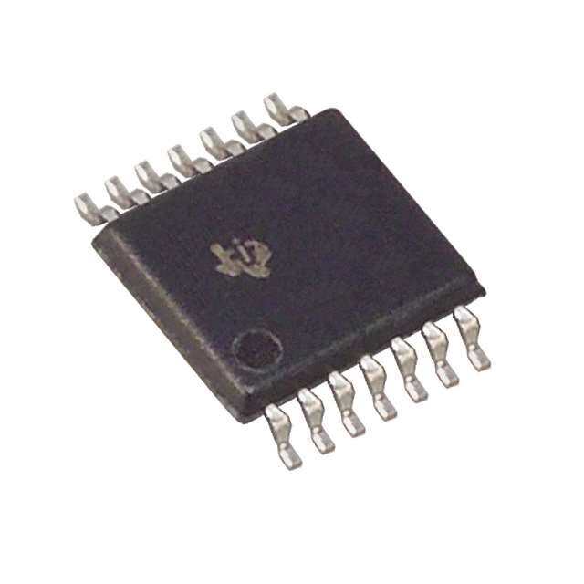
| 描述 | IC D-TYPE POS TRG DUAL 14SOIC触发器 Dual Pos Edge Trig |
| 产品分类 | |
| 品牌 | Texas Instruments |
| 产品手册 | |
| 产品图片 |
|
| rohs | 符合RoHS无铅 / 符合限制有害物质指令(RoHS)规范要求 |
| 产品系列 | 逻辑集成电路,触发器,Texas Instruments SN74ACT74DR74ACT |
| 数据手册 | |
| 产品型号 | SN74ACT74DR |
| 不同V、最大CL时的最大传播延迟 | 7.5ns @ 5V,50pF |
| 产品目录页面 | |
| 产品种类 | 触发器 |
| 传播延迟时间 | 11 ns |
| 低电平输出电流 | 24 mA |
| 元件数 | 2 |
| 其它名称 | 296-1079-1 |
| 功能 | 设置(预设)和复位 |
| 包装 | 剪切带 (CT) |
| 单位重量 | 129.400 mg |
| 商标 | Texas Instruments |
| 安装类型 | 表面贴装 |
| 安装风格 | SMD/SMT |
| 封装 | Reel |
| 封装/外壳 | 14-SOIC(0.154",3.90mm 宽) |
| 封装/箱体 | SOIC-14 |
| 工作温度 | -40°C ~ 85°C |
| 工厂包装数量 | 2500 |
| 最大工作温度 | + 85 C |
| 最小工作温度 | - 40 C |
| 极性 | Inverting/Non-Inverting |
| 标准包装 | 1 |
| 每元件位数 | 1 |
| 电压-电源 | 4.5 V ~ 5.5 V |
| 电流-输出高,低 | 24mA,24mA |
| 电流-静态 | 2µA |
| 电源电压-最大 | 5.5 V |
| 电源电压-最小 | 4.5 V |
| 电路数量 | 2 |
| 类型 | D 型 |
| 系列 | SN74ACT74 |
| 触发器类型 | 正边沿 |
| 输入电容 | 3pF |
| 输入类型 | TTL |
| 输入线路数量 | 4 |
| 输出类型 | 差分 |
| 输出线路数量 | 2 |
| 逻辑类型 | D-Type Flip-Flop |
| 逻辑系列 | ACT |
| 频率-时钟 | 210MHz |
| 高电平输出电流 | - 24 mA |


- 商务部:美国ITC正式对集成电路等产品启动337调查
- 曝三星4nm工艺存在良率问题 高通将骁龙8 Gen1或转产台积电
- 太阳诱电将投资9.5亿元在常州建新厂生产MLCC 预计2023年完工
- 英特尔发布欧洲新工厂建设计划 深化IDM 2.0 战略
- 台积电先进制程称霸业界 有大客户加持明年业绩稳了
- 达到5530亿美元!SIA预计今年全球半导体销售额将创下新高
- 英特尔拟将自动驾驶子公司Mobileye上市 估值或超500亿美元
- 三星加码芯片和SET,合并消费电子和移动部门,撤换高东真等 CEO
- 三星电子宣布重大人事变动 还合并消费电子和移动部门
- 海关总署:前11个月进口集成电路产品价值2.52万亿元 增长14.8%


PDF Datasheet 数据手册内容提取
(cid:1)(cid:2)(cid:3)(cid:4)(cid:5)(cid:6)(cid:7)(cid:8)(cid:4)(cid:9) (cid:1)(cid:2)(cid:8)(cid:4)(cid:5)(cid:6)(cid:7)(cid:8)(cid:4) (cid:10)(cid:11)(cid:5)(cid:12) (cid:13)(cid:14)(cid:1)(cid:15)(cid:7)(cid:15)(cid:16)(cid:17)(cid:18)(cid:17)(cid:10)(cid:19)(cid:17)(cid:18)(cid:7)(cid:20)(cid:15)(cid:19)(cid:19)(cid:17)(cid:20)(cid:17)(cid:10) (cid:10)(cid:18)(cid:7)(cid:21)(cid:13)(cid:17) (cid:22)(cid:12)(cid:15)(cid:13)(cid:18)(cid:22)(cid:12)(cid:14)(cid:13)(cid:1) (cid:23)(cid:15)(cid:7)(cid:24) (cid:6)(cid:12)(cid:17)(cid:5)(cid:20) (cid:5)(cid:2)(cid:10) (cid:13)(cid:20)(cid:17)(cid:1)(cid:17)(cid:7) SCAS520H − AUGUST 1995 − REVISED OCTOBER 2003 (cid:1) (cid:1) 4.5-V to 5.5-V V Operation Max t of 10.5 ns at 5 V CC pd (cid:1) (cid:1) Inputs Accept Voltages to 5.5 V Inputs Are TTL-Voltage Compatible SN54ACT74 ...J OR W PACKAGE SN54ACT74...FK PACKAGE SN74ACT74 ...D, DB, N, NS, OR PW PACKAGE (TOP VIEW) (TOP VIEW) R R L CL D C C CC 1CLR 1 14 VCC 1 1 NV 2 1D 2 13 2CLR 3 2 1 20 19 1CLK 3 12 2D 1CLK 4 18 2D 1PRE 4 11 2CLK NC 5 17 NC 1Q 5 10 2PRE 1PRE 6 16 2CLK 1Q 6 9 2Q NC 7 15 NC GND 7 8 2Q 1Q 8 14 2PRE 9 10 11 12 13 Q D CQ Q 1 N N2 2 G NC − No internal connection description/ordering information The ’ACT74 dual positive-edge-triggered devices are D-type flip-flops. A low level at the preset (PRE) or clear (CLR) input sets or resets the outputs, regardless of the levels of the other inputs. When PRE and CLR are inactive (high), data at the data (D) input meeting the setup-time requirements is transferred to the outputs on the positive-going edge of the clock pulse. Clock triggering occurs at a voltage level and is not directly related to the rise time of the clock pulse. Following the hold-time interval, data at D can be changed without affecting the levels at the outputs. ORDERING INFORMATION ORDERABLE TOP-SIDE TA PACKAGE† PART NUMBER MARKING PDIP − N Tube SN74ACT74N SN74ACT74N Tube SN74ACT74D SSOOIICC −− DD AACCTT7744 Tape and reel SN74ACT74DR −−4400°CC ttoo 8855°CC SOP − NS Tape and reel SN74ACT74NSR ACT74 SSOP − DB Tape and reel SN74ACT74DBR AD74 Tube SN74ACT74PW TTSSSSOOPP −− PPWW AADD7744 Tape and reel SN74ACT74PWR CDIP − J Tube SNJ54ACT74J SNJ54ACT74J −−5555°CC ttoo 112255°CC CFP − W Tube SNJ54ACT74W SNJ54ACT74W LCCC − FK Tube SNJ54ACT74FK SNJ54ACT74FK †Package drawings, standard packing quantities, thermal data, symbolization, and PCB design guidelines are available at www.ti.com/sc/package. Please be aware that an important notice concerning availability, standard warranty, and use in critical applications of TexasInstruments semiconductor products and disclaimers thereto appears at the end of this data sheet. (cid:13)(cid:20)(cid:14)(cid:10)(cid:11)(cid:6)(cid:7)(cid:15)(cid:14)(cid:2) (cid:10)(cid:5)(cid:7)(cid:5) (cid:25)(cid:26)(cid:27)(cid:28)(cid:29)(cid:30)(cid:31)!(cid:25)(cid:28)(cid:26) (cid:25)" #$(cid:29)(cid:29)%(cid:26)! (cid:31)" (cid:28)(cid:27) &$’((cid:25)#(cid:31)!(cid:25)(cid:28)(cid:26) )(cid:31)!%* Copyright 2003, Texas Instruments Incorporated (cid:13)(cid:29)(cid:28))$#!" #(cid:28)(cid:26)(cid:27)(cid:28)(cid:29)(cid:30) !(cid:28) "&%#(cid:25)(cid:27)(cid:25)#(cid:31)!(cid:25)(cid:28)(cid:26)" &%(cid:29) !+% !%(cid:29)(cid:30)" (cid:28)(cid:27) (cid:7)%,(cid:31)" (cid:15)(cid:26)"!(cid:29)$(cid:30)%(cid:26)!" (cid:14)(cid:26) &(cid:29)(cid:28))$#!" #(cid:28)(cid:30)&((cid:25)(cid:31)(cid:26)! !(cid:28) 0(cid:15)(cid:12)(cid:18)(cid:13)(cid:20)(cid:22)(cid:18)12(cid:3)1(cid:3)(cid:9) (cid:31)(( &(cid:31)(cid:29)(cid:31)(cid:30)%!%(cid:29)" (cid:31)(cid:29)% !%"!%) "!(cid:31)(cid:26))(cid:31)(cid:29)) -(cid:31)(cid:29)(cid:29)(cid:31)(cid:26)!.* (cid:13)(cid:29)(cid:28))$#!(cid:25)(cid:28)(cid:26) &(cid:29)(cid:28)#%""(cid:25)(cid:26)/ )(cid:28)%" (cid:26)(cid:28)! (cid:26)%#%""(cid:31)(cid:29)(cid:25)(. (cid:25)(cid:26)#($)% $(cid:26)(%"" (cid:28)!+%(cid:29)-(cid:25)"% (cid:26)(cid:28)!%)* (cid:14)(cid:26) (cid:31)(( (cid:28)!+%(cid:29) &(cid:29)(cid:28))$#!"(cid:9) &(cid:29)(cid:28))$#!(cid:25)(cid:28)(cid:26) !%"!(cid:25)(cid:26)/ (cid:28)(cid:27) (cid:31)(( &(cid:31)(cid:29)(cid:31)(cid:30)%!%(cid:29)"* &(cid:29)(cid:28)#%""(cid:25)(cid:26)/ )(cid:28)%" (cid:26)(cid:28)! (cid:26)%#%""(cid:31)(cid:29)(cid:25)(. (cid:25)(cid:26)#($)% !%"!(cid:25)(cid:26)/ (cid:28)(cid:27) (cid:31)(( &(cid:31)(cid:29)(cid:31)(cid:30)%!%(cid:29)"* POST OFFICE BOX 655303 • DALLAS, TEXAS 75265 1
(cid:1)(cid:2)(cid:3)(cid:4)(cid:5)(cid:6)(cid:7)(cid:8)(cid:4)(cid:9) (cid:1)(cid:2)(cid:8)(cid:4)(cid:5)(cid:6)(cid:7)(cid:8)(cid:4) (cid:10)(cid:11)(cid:5)(cid:12) (cid:13)(cid:14)(cid:1)(cid:15)(cid:7)(cid:15)(cid:16)(cid:17)(cid:18)(cid:17)(cid:10)(cid:19)(cid:17)(cid:18)(cid:7)(cid:20)(cid:15)(cid:19)(cid:19)(cid:17)(cid:20)(cid:17)(cid:10) (cid:10)(cid:18)(cid:7)(cid:21)(cid:13)(cid:17) (cid:22)(cid:12)(cid:15)(cid:13)(cid:18)(cid:22)(cid:12)(cid:14)(cid:13)(cid:1) (cid:23)(cid:15)(cid:7)(cid:24) (cid:6)(cid:12)(cid:17)(cid:5)(cid:20) (cid:5)(cid:2)(cid:10) (cid:13)(cid:20)(cid:17)(cid:1)(cid:17)(cid:7) SCAS520H − AUGUST 1995 − REVISED OCTOBER 2003 FUNCTION TABLE (each flip-flop) INPUTS OUTPUTS PRE CLR CLK D Q Q L H X X H L H L X X L H L L X X H† H† H H ↑ H H L H H ↑ L L H H H L X Q0 Q0 †This configuration is nonstable; that is, it does not persist when either PRE or CLR returns to its inactive (high) level. logic diagram, each flip-flop (positive logic) PRE CLK C C C Q TG C C C C D TG TG TG Q C C C CLR 2 POST OFFICE BOX 655303 • DALLAS, TEXAS 75265
(cid:1)(cid:2)(cid:3)(cid:4)(cid:5)(cid:6)(cid:7)(cid:8)(cid:4)(cid:9) (cid:1)(cid:2)(cid:8)(cid:4)(cid:5)(cid:6)(cid:7)(cid:8)(cid:4) (cid:10)(cid:11)(cid:5)(cid:12) (cid:13)(cid:14)(cid:1)(cid:15)(cid:7)(cid:15)(cid:16)(cid:17)(cid:18)(cid:17)(cid:10)(cid:19)(cid:17)(cid:18)(cid:7)(cid:20)(cid:15)(cid:19)(cid:19)(cid:17)(cid:20)(cid:17)(cid:10) (cid:10)(cid:18)(cid:7)(cid:21)(cid:13)(cid:17) (cid:22)(cid:12)(cid:15)(cid:13)(cid:18)(cid:22)(cid:12)(cid:14)(cid:13)(cid:1) (cid:23)(cid:15)(cid:7)(cid:24) (cid:6)(cid:12)(cid:17)(cid:5)(cid:20) (cid:5)(cid:2)(cid:10) (cid:13)(cid:20)(cid:17)(cid:1)(cid:17)(cid:7) SCAS520H − AUGUST 1995 − REVISED OCTOBER 2003 absolute maximum ratings over operating free-air temperature range (unless otherwise noted)† Supply voltage range, V . . . . . . . . . . . . . . . . . . . . . . . . . . . . . . . . . . . . . . . . . . . . . . . . . . . . . . . . . . −0.5 V to 7 V CC Input voltage range, VI (see Note 1) . . . . . . . . . . . . . . . . . . . . . . . . . . . . . . . . . . . . . . . . . . . −0.5 V to VCC + 0.5 V Output voltage range, V (see Note 1) . . . . . . . . . . . . . . . . . . . . . . . . . . . . . . . . . . . . . . . . −0.5 V to V + 0.5 V O CC Input clamp current, I (V < 0 or V > V ) . . . . . . . . . . . . . . . . . . . . . . . . . . . . . . . . . . . . . . . . . . . . . . . . ±20 mA IK I I CC Output clamp current, I (V < 0 or V > V ) . . . . . . . . . . . . . . . . . . . . . . . . . . . . . . . . . . . . . . . . . . . . ±20 mA OK O O CC Continuous output current, I (V = 0 to V ) . . . . . . . . . . . . . . . . . . . . . . . . . . . . . . . . . . . . . . . . . . . . . . ±50 mA O O CC Continuous current through V or GND . . . . . . . . . . . . . . . . . . . . . . . . . . . . . . . . . . . . . . . . . . . . . . . . . . ±200 mA CC Package thermal impedance, θ (see Note 2): D package . . . . . . . . . . . . . . . . . . . . . . . . . . . . . . . . . . . 86°C/W JA DB package . . . . . . . . . . . . . . . . . . . . . . . . . . . . . . . . . 96°C/W N package . . . . . . . . . . . . . . . . . . . . . . . . . . . . . . . . . . . 80°C/W NS package . . . . . . . . . . . . . . . . . . . . . . . . . . . . . . . . . 76°C/W PW package . . . . . . . . . . . . . . . . . . . . . . . . . . . . . . . . 113°C/W Storage temperature range, T . . . . . . . . . . . . . . . . . . . . . . . . . . . . . . . . . . . . . . . . . . . . . . . . . . . −65°C to 150°C stg †Stresses beyond those listed under “absolute maximum ratings” may cause permanent damage to the device. These are stress ratings only, and functional operation of the device at these or any other conditions beyond those indicated under “recommended operating conditions” is not implied. Exposure to absolute-maximum-rated conditions for extended periods may affect device reliability. NOTES: 1. The input and output voltage ratings may be exceeded if the input and output current ratings are observed. 2. The package thermal impedance is calculated in accordance with JESD 51-7. recommended operating conditions (see Note 3) SN54ACT74 SN74ACT74 UUNNIITT MIN MAX MIN MAX VCC Supply voltage 4.5 5.5 4.5 5.5 V VIH High-level input voltage 2 2 V VIL Low-level input voltage 0.8 0.8 V VI Input voltage 0 VCC 0 VCC V VO Output voltage 0 VCC 0 VCC V IOH High-level output current −24 −24 mA IOL Low-level output current 24 24 mA ∆t/∆v Input transition rise or fall rate 8 8 ns/V TA Operating free-air temperature −55 125 −40 85 °C NOTE 3: All unused inputs of the device must be held at VCC or GND to ensure proper device operation. Refer to the TI application report, Implications of Slow or Floating CMOS Inputs, literature number SCBA004. POST OFFICE BOX 655303 • DALLAS, TEXAS 75265 3
(cid:1)(cid:2)(cid:3)(cid:4)(cid:5)(cid:6)(cid:7)(cid:8)(cid:4)(cid:9) (cid:1)(cid:2)(cid:8)(cid:4)(cid:5)(cid:6)(cid:7)(cid:8)(cid:4) (cid:10)(cid:11)(cid:5)(cid:12) (cid:13)(cid:14)(cid:1)(cid:15)(cid:7)(cid:15)(cid:16)(cid:17)(cid:18)(cid:17)(cid:10)(cid:19)(cid:17)(cid:18)(cid:7)(cid:20)(cid:15)(cid:19)(cid:19)(cid:17)(cid:20)(cid:17)(cid:10) (cid:10)(cid:18)(cid:7)(cid:21)(cid:13)(cid:17) (cid:22)(cid:12)(cid:15)(cid:13)(cid:18)(cid:22)(cid:12)(cid:14)(cid:13)(cid:1) (cid:23)(cid:15)(cid:7)(cid:24) (cid:6)(cid:12)(cid:17)(cid:5)(cid:20) (cid:5)(cid:2)(cid:10) (cid:13)(cid:20)(cid:17)(cid:1)(cid:17)(cid:7) SCAS520H − AUGUST 1995 − REVISED OCTOBER 2003 electrical characteristics over recommended operating free-air temperature range (unless otherwise noted) TA = 25°C SN54ACT74 SN74ACT74 PPAARRAAMMEETTEERR TTEESSTT CCOONNDDIITTIIOONNSS VVCCCC UUNNIITT MIN TYP MAX MIN MAX MIN MAX 4.5 V 4.4 4.49 4.4 4.4 IIOOHH == −−5500 µAA 5.5 V 5.4 5.49 5.4 5.4 4.5 V 3.86 3.7 3.76 VVOOHH IIOOHH == −−2244 mmAA VV 5.5 V 4.86 4.7 4.76 IOH = −50 mA† 5.5 V 3.86 IOH = −75 mA† 5.5 V 3.85 4.5 V 0.001 0.1 0.1 0.1 IIOOLL == 5500 µAA 5.5 V 0.001 0.1 0.1 0.1 4.5 V 0.36 0.5 0.44 VVOOLL IIOOLL == 2244 mmAA VV 5.5 V 0.36 0.5 0.44 IOL = 50 mA† 5.5 V 1.65 IOL = 75 mA† 5.5 V 1.65 II VI = VCC or GND 5.5 V ±0.1 ±1 ±1 µA ICC VI = VCC or GND, IO = 0 5.5 V 2 40 20 µA One input at 3.4 V, ∆ICC‡ Other inputs at GND or VCC 5.5 V 0.6 1.6 1.5 mA Ci VI = VCC or GND 5 V 3 pF †Not more than one output should be tested at a time, and the duration of the test should not exceed 2 ms. ‡This is the increase in supply current for each input that is at one of the specified TTL voltage levels, rather than 0 V or VCC. timing characteristics over recommended ranges of supply voltage and operating free-air temperature (unless otherwise noted) (see Figure 1) TA = 25°C SN54ACT74 SN74ACT74 UUNNIITT MIN MAX MIN MAX MIN MAX fclock Clock frequency 145 85 125 MHz PRE or CLR low 5 7 6 ttww PPuullssee dduurraattiioonn nnss CLK 5 7 6 Data 3 4 3.5 ttssuu SSeettuupp ttiimmee,, ddaattaa bbeeffoorree CCLLKK↑↑ nnss PRE or CLR inactive 0 0.5 0 th Hold time, data after CLK↑ 1 1 1 ns switching characteristics over recommended operating free-air temperature (unless otherwise noted) (see Figure 1) SN54ACT74 FFRROOMM TTOO PPAARRAAMMEETTEERR TA = 25°C UUNNIITT ((IINNPPUUTT)) ((OOUUTTPPUUTT)) MMIINN MMAAXX MIN TYP MAX fmax 145 210 85 MHz tPLH 1 5.5 9.5 1 11.5 PPRREE oorr CCLLRR QQ oorr QQ nnss tPHL 1 6 10 1 12.5 tPLH 1 7.5 11 1 14 CCLLKK QQ oorr QQ nnss tPHL 1 6 10 1 12 4 POST OFFICE BOX 655303 • DALLAS, TEXAS 75265
(cid:1)(cid:2)(cid:3)(cid:4)(cid:5)(cid:6)(cid:7)(cid:8)(cid:4)(cid:9) (cid:1)(cid:2)(cid:8)(cid:4)(cid:5)(cid:6)(cid:7)(cid:8)(cid:4) (cid:10)(cid:11)(cid:5)(cid:12) (cid:13)(cid:14)(cid:1)(cid:15)(cid:7)(cid:15)(cid:16)(cid:17)(cid:18)(cid:17)(cid:10)(cid:19)(cid:17)(cid:18)(cid:7)(cid:20)(cid:15)(cid:19)(cid:19)(cid:17)(cid:20)(cid:17)(cid:10) (cid:10)(cid:18)(cid:7)(cid:21)(cid:13)(cid:17) (cid:22)(cid:12)(cid:15)(cid:13)(cid:18)(cid:22)(cid:12)(cid:14)(cid:13)(cid:1) (cid:23)(cid:15)(cid:7)(cid:24) (cid:6)(cid:12)(cid:17)(cid:5)(cid:20) (cid:5)(cid:2)(cid:10) (cid:13)(cid:20)(cid:17)(cid:1)(cid:17)(cid:7) SCAS520H − AUGUST 1995 − REVISED OCTOBER 2003 switching characteristics over recommended operating free-air temperature (unless otherwise noted) (see Figure 1) SN74ACT74 FFRROOMM TTOO PPAARRAAMMEETTEERR TA = 25°C UUNNIITT ((IINNPPUUTT)) ((OOUUTTPPUUTT)) MMIINN MMAAXX MIN TYP MAX fmax 145 210 125 MHz tPLH 3 5.5 9.5 2.5 10.5 PPRREE oorr CCLLRR QQ oorr QQ nnss tPHL 3 6 10 3 11.5 tPLH 4 7.5 11 4 13 CCLLKK QQ oorr QQ nnss tPHL 3.5 6 10 3 11.5 operating characteristics, VCC = 5 V, TA = 25°C PARAMETER TEST CONDITIONS TYP UNIT Cpd Power dissipation capacitance CL = 50 pF, f = 1 MHz 45 pF PARAMETER MEASUREMENT INFORMATION 2 × VCC 500 Ω S1 Open From Output Under Test TEST S1 CL = 50 pF 500 Ω tPLH/tPHL Open (see Note A) tw LOAD CIRCUIT 3 V Input 1.5 V 1.5 V 3 V Input 1.5 V 1.5 V 0 V 0 V VOLTAGE WAVEFORMS tPLH tPHL VOH In-Phase 3 V Output 50% VCC 50% VCC Timing Input 1.5 V VOL 0 V tPHL tPLH tsu th VOH 3 V Out-of-Phase 50% VCC 50% VCC Data Input 1.5 V 1.5 V Output VOL 0 V VOLTAGE WAVEFORMS VOLTAGE WAVEFORMS NOTES:A. CL includes probe and jig capacitance. B. All input pulses are supplied by generators having the following characteristics: PRR ≤ 1 MHz, ZO = 50 Ω, tr ≤2.5 ns, tf ≤ 2.5 ns. C. The outputs are measured one at a time with one input transition per measurement. Figure 1. Load Circuit and Voltage Waveforms POST OFFICE BOX 655303 • DALLAS, TEXAS 75265 5
PACKAGE OPTION ADDENDUM www.ti.com 24-Aug-2018 PACKAGING INFORMATION Orderable Device Status Package Type Package Pins Package Eco Plan Lead/Ball Finish MSL Peak Temp Op Temp (°C) Device Marking Samples (1) Drawing Qty (2) (6) (3) (4/5) 5962-8752501M2A ACTIVE LCCC FK 20 1 TBD POST-PLATE N / A for Pkg Type -55 to 125 5962- 8752501M2A SNJ54ACT 74FK 5962-8752501MCA ACTIVE CDIP J 14 1 TBD A42 N / A for Pkg Type -55 to 125 5962-8752501MC A SNJ54ACT74J 5962-8752501MDA ACTIVE CFP W 14 1 TBD A42 N / A for Pkg Type -55 to 125 5962-8752501MD A SNJ54ACT74W SN74ACT74D ACTIVE SOIC D 14 50 Green (RoHS CU NIPDAU Level-1-260C-UNLIM -40 to 85 ACT74 & no Sb/Br) SN74ACT74DBR ACTIVE SSOP DB 14 2000 Green (RoHS CU NIPDAU Level-1-260C-UNLIM -40 to 85 AD74 & no Sb/Br) SN74ACT74DE4 ACTIVE SOIC D 14 50 Green (RoHS CU NIPDAU Level-1-260C-UNLIM -40 to 85 ACT74 & no Sb/Br) SN74ACT74DG4 ACTIVE SOIC D 14 50 Green (RoHS CU NIPDAU Level-1-260C-UNLIM -40 to 85 ACT74 & no Sb/Br) SN74ACT74DR ACTIVE SOIC D 14 2500 Green (RoHS CU NIPDAU Level-1-260C-UNLIM -40 to 85 ACT74 & no Sb/Br) SN74ACT74DRE4 ACTIVE SOIC D 14 2500 Green (RoHS CU NIPDAU Level-1-260C-UNLIM -40 to 85 ACT74 & no Sb/Br) SN74ACT74DRG4 ACTIVE SOIC D 14 2500 Green (RoHS CU NIPDAU Level-1-260C-UNLIM -40 to 85 ACT74 & no Sb/Br) SN74ACT74N ACTIVE PDIP N 14 25 Green (RoHS CU NIPDAU N / A for Pkg Type -40 to 85 SN74ACT74N & no Sb/Br) SN74ACT74NE4 ACTIVE PDIP N 14 25 Green (RoHS CU NIPDAU N / A for Pkg Type -40 to 85 SN74ACT74N & no Sb/Br) SN74ACT74NSR ACTIVE SO NS 14 2000 Green (RoHS CU NIPDAU Level-1-260C-UNLIM -40 to 85 ACT74 & no Sb/Br) SN74ACT74PW ACTIVE TSSOP PW 14 90 Green (RoHS CU NIPDAU Level-1-260C-UNLIM -40 to 85 AD74 & no Sb/Br) SN74ACT74PWR ACTIVE TSSOP PW 14 2000 Green (RoHS CU NIPDAU Level-1-260C-UNLIM -40 to 85 AD74 & no Sb/Br) Addendum-Page 1
PACKAGE OPTION ADDENDUM www.ti.com 24-Aug-2018 Orderable Device Status Package Type Package Pins Package Eco Plan Lead/Ball Finish MSL Peak Temp Op Temp (°C) Device Marking Samples (1) Drawing Qty (2) (6) (3) (4/5) SN74ACT74PWRE4 ACTIVE TSSOP PW 14 2000 Green (RoHS CU NIPDAU Level-1-260C-UNLIM -40 to 85 AD74 & no Sb/Br) SNJ54ACT74FK ACTIVE LCCC FK 20 1 TBD POST-PLATE N / A for Pkg Type -55 to 125 5962- 8752501M2A SNJ54ACT 74FK SNJ54ACT74J ACTIVE CDIP J 14 1 TBD A42 N / A for Pkg Type -55 to 125 5962-8752501MC A SNJ54ACT74J SNJ54ACT74W ACTIVE CFP W 14 1 TBD A42 N / A for Pkg Type -55 to 125 5962-8752501MD A SNJ54ACT74W (1) The marketing status values are defined as follows: ACTIVE: Product device recommended for new designs. LIFEBUY: TI has announced that the device will be discontinued, and a lifetime-buy period is in effect. NRND: Not recommended for new designs. Device is in production to support existing customers, but TI does not recommend using this part in a new design. PREVIEW: Device has been announced but is not in production. Samples may or may not be available. OBSOLETE: TI has discontinued the production of the device. (2) RoHS: TI defines "RoHS" to mean semiconductor products that are compliant with the current EU RoHS requirements for all 10 RoHS substances, including the requirement that RoHS substance do not exceed 0.1% by weight in homogeneous materials. Where designed to be soldered at high temperatures, "RoHS" products are suitable for use in specified lead-free processes. TI may reference these types of products as "Pb-Free". RoHS Exempt: TI defines "RoHS Exempt" to mean products that contain lead but are compliant with EU RoHS pursuant to a specific EU RoHS exemption. Green: TI defines "Green" to mean the content of Chlorine (Cl) and Bromine (Br) based flame retardants meet JS709B low halogen requirements of <=1000ppm threshold. Antimony trioxide based flame retardants must also meet the <=1000ppm threshold requirement. (3) MSL, Peak Temp. - The Moisture Sensitivity Level rating according to the JEDEC industry standard classifications, and peak solder temperature. (4) There may be additional marking, which relates to the logo, the lot trace code information, or the environmental category on the device. (5) Multiple Device Markings will be inside parentheses. Only one Device Marking contained in parentheses and separated by a "~" will appear on a device. If a line is indented then it is a continuation of the previous line and the two combined represent the entire Device Marking for that device. (6) Lead/Ball Finish - Orderable Devices may have multiple material finish options. Finish options are separated by a vertical ruled line. Lead/Ball Finish values may wrap to two lines if the finish value exceeds the maximum column width. Addendum-Page 2
PACKAGE OPTION ADDENDUM www.ti.com 24-Aug-2018 Important Information and Disclaimer:The information provided on this page represents TI's knowledge and belief as of the date that it is provided. TI bases its knowledge and belief on information provided by third parties, and makes no representation or warranty as to the accuracy of such information. Efforts are underway to better integrate information from third parties. TI has taken and continues to take reasonable steps to provide representative and accurate information but may not have conducted destructive testing or chemical analysis on incoming materials and chemicals. TI and TI suppliers consider certain information to be proprietary, and thus CAS numbers and other limited information may not be available for release. In no event shall TI's liability arising out of such information exceed the total purchase price of the TI part(s) at issue in this document sold by TI to Customer on an annual basis. OTHER QUALIFIED VERSIONS OF SN54ACT74, SN74ACT74 : •Catalog: SN74ACT74 •Enhanced Product: SN74ACT74-EP, SN74ACT74-EP •Military: SN54ACT74 NOTE: Qualified Version Definitions: •Catalog - TI's standard catalog product •Enhanced Product - Supports Defense, Aerospace and Medical Applications •Military - QML certified for Military and Defense Applications Addendum-Page 3
PACKAGE MATERIALS INFORMATION www.ti.com 20-Dec-2018 TAPE AND REEL INFORMATION *Alldimensionsarenominal Device Package Package Pins SPQ Reel Reel A0 B0 K0 P1 W Pin1 Type Drawing Diameter Width (mm) (mm) (mm) (mm) (mm) Quadrant (mm) W1(mm) SN74ACT74DR SOIC D 14 2500 330.0 16.4 6.5 9.0 2.1 8.0 16.0 Q1 SN74ACT74NSR SO NS 14 2000 330.0 16.4 8.2 10.5 2.5 12.0 16.0 Q1 SN74ACT74PWR TSSOP PW 14 2000 330.0 12.4 6.9 5.6 1.6 8.0 12.0 Q1 PackMaterials-Page1
PACKAGE MATERIALS INFORMATION www.ti.com 20-Dec-2018 *Alldimensionsarenominal Device PackageType PackageDrawing Pins SPQ Length(mm) Width(mm) Height(mm) SN74ACT74DR SOIC D 14 2500 367.0 367.0 38.0 SN74ACT74NSR SO NS 14 2000 367.0 367.0 38.0 SN74ACT74PWR TSSOP PW 14 2000 367.0 367.0 35.0 PackMaterials-Page2
None
None
None
None
PACKAGE OUTLINE J0014A CDIP - 5.08 mm max height SCALE 0.900 CERAMIC DUAL IN LINE PACKAGE PIN 1 ID A 4X .005 MIN (OPTIONAL) [0.13] .015-.060 TYP [0.38-1.52] 1 14 12X .100 [2.54] 14X .014-.026 14X .045-.065 [0.36-0.66] [1.15-1.65] .010 [0.25] C A B .754-.785 [19.15-19.94] 7 8 B .245-.283 .2 MAX TYP .13 MIN TYP [6.22-7.19] [5.08] [3.3] SEATING PLANE C .308-.314 [7.83-7.97] AT GAGE PLANE .015 GAGE PLANE [0.38] 0 -15 14X .008-.014 TYP [0.2-0.36] 4214771/A 05/2017 NOTES: 1. All controlling linear dimensions are in inches. Dimensions in brackets are in millimeters. Any dimension in brackets or parenthesis are for reference only. Dimensioning and tolerancing per ASME Y14.5M. 2. This drawing is subject to change without notice. 3. This package is hermitically sealed with a ceramic lid using glass frit. 4. Index point is provided on cap for terminal identification only and on press ceramic glass frit seal only. 5. Falls within MIL-STD-1835 and GDIP1-T14. www.ti.com
EXAMPLE BOARD LAYOUT J0014A CDIP - 5.08 mm max height CERAMIC DUAL IN LINE PACKAGE (.300 ) TYP [7.62] SEE DETAIL B SEE DETAIL A 1 14 12X (.100 ) [2.54] SYMM 14X ( .039) [1] 7 8 SYMM LAND PATTERN EXAMPLE NON-SOLDER MASK DEFINED SCALE: 5X .002 MAX (.063) [0.05] [1.6] METAL ALL AROUND ( .063) SOLDER MASK [1.6] OPENING METAL .002 MAX SOLDER MASK (R.002 ) TYP [0.05] OPENING [0.05] ALL AROUND DETAIL A DETAIL B SCALE: 15X 13X, SCALE: 15X 4214771/A 05/2017 www.ti.com
None
None
None
None
None
MECHANICAL DATA MSSO002E – JANUARY 1995 – REVISED DECEMBER 2001 DB (R-PDSO-G**) PLASTIC SMALL-OUTLINE 28 PINS SHOWN 0,38 0,65 0,15 M 0,22 28 15 0,25 0,09 5,60 8,20 5,00 7,40 Gage Plane 1 14 0,25 A 0°–(cid:1)8° 0,95 0,55 Seating Plane 2,00 MAX 0,05 MIN 0,10 PINS ** 14 16 20 24 28 30 38 DIM A MAX 6,50 6,50 7,50 8,50 10,50 10,50 12,90 A MIN 5,90 5,90 6,90 7,90 9,90 9,90 12,30 4040065/E 12/01 NOTES: A. All linear dimensions are in millimeters. B. This drawing is subject to change without notice. C. Body dimensions do not include mold flash or protrusion not to exceed 0,15. D. Falls within JEDEC MO-150 • POST OFFICE BOX 655303 DALLAS, TEXAS 75265
IMPORTANTNOTICEANDDISCLAIMER TIPROVIDESTECHNICALANDRELIABILITYDATA(INCLUDINGDATASHEETS),DESIGNRESOURCES(INCLUDINGREFERENCE DESIGNS),APPLICATIONOROTHERDESIGNADVICE,WEBTOOLS,SAFETYINFORMATION,ANDOTHERRESOURCES“ASIS” ANDWITHALLFAULTS,ANDDISCLAIMSALLWARRANTIES,EXPRESSANDIMPLIED,INCLUDINGWITHOUTLIMITATIONANY IMPLIEDWARRANTIESOFMERCHANTABILITY,FITNESSFORAPARTICULARPURPOSEORNON-INFRINGEMENTOFTHIRD PARTYINTELLECTUALPROPERTYRIGHTS. TheseresourcesareintendedforskilleddevelopersdesigningwithTIproducts.Youaresolelyresponsiblefor(1)selectingtheappropriate TIproductsforyourapplication,(2)designing,validatingandtestingyourapplication,and(3)ensuringyourapplicationmeetsapplicable standards,andanyothersafety,security,orotherrequirements.Theseresourcesaresubjecttochangewithoutnotice.TIgrantsyou permissiontousetheseresourcesonlyfordevelopmentofanapplicationthatusestheTIproductsdescribedintheresource.Other reproductionanddisplayoftheseresourcesisprohibited.NolicenseisgrantedtoanyotherTIintellectualpropertyrightortoanythird partyintellectualpropertyright.TIdisclaimsresponsibilityfor,andyouwillfullyindemnifyTIanditsrepresentativesagainst,anyclaims, damages,costs,losses,andliabilitiesarisingoutofyouruseoftheseresources. TI’sproductsareprovidedsubjecttoTI’sTermsofSale(www.ti.com/legal/termsofsale.html)orotherapplicabletermsavailableeitheron ti.comorprovidedinconjunctionwithsuchTIproducts.TI’sprovisionoftheseresourcesdoesnotexpandorotherwisealterTI’sapplicable warrantiesorwarrantydisclaimersforTIproducts. MailingAddress:TexasInstruments,PostOfficeBox655303,Dallas,Texas75265 Copyright©2018,TexasInstrumentsIncorporated