ICGOO在线商城 > 集成电路(IC) > 逻辑 - 栅极和逆变器 > SN74AC00N
 Datasheet下载
- 型号: SN74AC00N
- 制造商: Texas Instruments
- 库位|库存: xxxx|xxxx
- 要求:
| 数量阶梯 | 香港交货 | 国内含税 |
| +xxxx | $xxxx | ¥xxxx |
查看当月历史价格
查看今年历史价格
SN74AC00N产品简介:
ICGOO电子元器件商城为您提供SN74AC00N由Texas Instruments设计生产,在icgoo商城现货销售,并且可以通过原厂、代理商等渠道进行代购。 SN74AC00N价格参考¥1.09-¥3.13。Texas InstrumentsSN74AC00N封装/规格:逻辑 - 栅极和逆变器, NAND Gate IC 4 Channel 14-PDIP。您可以下载SN74AC00N参考资料、Datasheet数据手册功能说明书,资料中有SN74AC00N 详细功能的应用电路图电压和使用方法及教程。
SN74AC00N是德州仪器(Texas Instruments)生产的一款逻辑电路芯片,具体属于四2输入与非门(NAND Gate)。它在数字电路设计中有着广泛的应用,主要应用于需要进行逻辑运算和信号处理的场合。以下是其应用场景的具体介绍:

1. 数字系统控制:SN74AC00N常用于构建复杂的数字控制系统,如微处理器、微控制器及外围设备之间的接口电路。通过组合多个NAND门可以实现更复杂的逻辑功能,如解码器、编码器等。

2. 时序电路设计:该器件可用于设计各种时序电路,包括但不限于触发器、计数器等。利用其快速开关特性和低功耗优势,能够有效提高系统的响应速度并降低能耗。

3. 通信设备中的应用:在通信领域,例如调制解调器或无线收发模块里,SN74AC00N可以用来生成同步信号或者作为数据传输路径上的关键组件之一,确保信息准确无误地传递。

4. 消费电子产品:从家用电器到个人电脑,许多消费级产品内部都会用到这类基础逻辑元件来完成特定任务,比如电源管理单元里的状态检测机制等。

5. 工业自动化:在工厂自动化生产线中,SN74AC00N可用于构建传感器网络节点间的通讯协议转换器,或是参与安全联锁保护系统的构建,保证生产设备的安全稳定运行。

6. 教育与科研实验:对于教学实验室而言,这款芯片是非常好的实践材料,学生可以通过搭建简单的逻辑电路来理解布尔代数原理及其实际应用;同时,在科研项目中也可以作为基础模块被集成进更复杂的原型系统中。

总之,SN74AC00N凭借其高性能参数(如高工作频率、低静态电流消耗等),成为众多电子工程师青睐的基础逻辑器件之一,在多个行业和技术领域都有重要的应用价值。
| 参数 | 数值 |
| 产品目录 | 集成电路 (IC)半导体 |
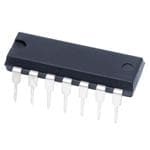
| 描述 | IC GATE NAND 4CH 2-INP 14-DIP逻辑门 Quad 2-Input |
| 产品分类 | |
| 品牌 | Texas Instruments |
| 产品手册 | |
| 产品图片 |
|
| rohs | 符合RoHS无铅 / 符合限制有害物质指令(RoHS)规范要求 |
| 产品系列 | 逻辑集成电路,逻辑门,Texas Instruments SN74AC00N74AC |
| 数据手册 | |
| 产品型号 | SN74AC00N |
| PCN设计/规格 | |
| 不同V、最大CL时的最大传播延迟 | 8ns @ 5V,50pF |
| 产品 | NAND |
| 产品目录页面 | |
| 产品种类 | 逻辑门 |
| 传播延迟时间 | 8.5 ns |
| 低电平输出电流 | 24 mA |
| 供应商器件封装 | 14-PDIP |
| 其它名称 | 296-4287-5 |
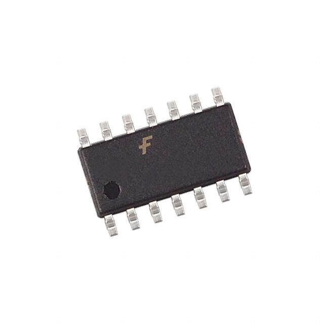
| 包装 | 管件 |
| 单位重量 | 1 g |
| 商标 | Texas Instruments |
| 安装类型 | 通孔 |
| 安装风格 | Through Hole |
| 封装 | Tube |
| 封装/外壳 | 14-DIP(0.300",7.62mm) |
| 封装/箱体 | PDIP-14 |
| 工作温度 | -40°C ~ 85°C |
| 工作温度范围 | - 40 C to + 85 C |
| 工厂包装数量 | 25 |
| 最大工作温度 | + 85 C |
| 最小工作温度 | - 40 C |
| 栅极数量 | 4 Gate |
| 标准包装 | 25 |
| 特性 | - |
| 电压-电源 | 2 V ~ 6 V |
| 电流-输出高,低 | 24mA,24mA |
| 电流-静态(最大值) | 2µA |
| 电源电压-最大 | 6 V |
| 电源电压-最小 | 2 V |
| 电路数 | 4 |
| 系列 | SN74AC00 |
| 输入/输出线数量 | 2 / 1 |
| 输入数 | 2 |
| 输入线路数量 | 2 |
| 输出电流 | 50 mA |
| 输出线路数量 | 1 |
| 逻辑电平-低 | 0.9 V ~ 1.65 V |
| 逻辑电平-高 | 2.1 V ~ 3.85 V |
| 逻辑类型 | 与非门 |
| 逻辑系列 | AC |
| 高电平输出电流 | - 24 mA |


- 商务部:美国ITC正式对集成电路等产品启动337调查
- 曝三星4nm工艺存在良率问题 高通将骁龙8 Gen1或转产台积电
- 太阳诱电将投资9.5亿元在常州建新厂生产MLCC 预计2023年完工
- 英特尔发布欧洲新工厂建设计划 深化IDM 2.0 战略
- 台积电先进制程称霸业界 有大客户加持明年业绩稳了
- 达到5530亿美元!SIA预计今年全球半导体销售额将创下新高
- 英特尔拟将自动驾驶子公司Mobileye上市 估值或超500亿美元
- 三星加码芯片和SET,合并消费电子和移动部门,撤换高东真等 CEO
- 三星电子宣布重大人事变动 还合并消费电子和移动部门
- 海关总署:前11个月进口集成电路产品价值2.52万亿元 增长14.8%


PDF Datasheet 数据手册内容提取
(cid:1)(cid:2)(cid:3)(cid:4)(cid:5)(cid:6)(cid:7)(cid:7)(cid:8) (cid:1)(cid:2)(cid:9)(cid:4)(cid:5)(cid:6)(cid:7)(cid:7) (cid:10)(cid:11)(cid:5)(cid:12)(cid:13)(cid:11)(cid:14)(cid:15)(cid:16) (cid:17)(cid:18)(cid:19)(cid:2)(cid:14)(cid:11)(cid:20) (cid:14)(cid:21)(cid:1)(cid:19)(cid:20)(cid:19)(cid:22)(cid:16)(cid:18)(cid:2)(cid:5)(cid:2)(cid:12) (cid:23)(cid:5)(cid:20)(cid:16)(cid:1) SCAS524E − AUGUST 1995 − REVISED OCTOBER 2003 (cid:1) 2-V to 6-V V Operation CC (cid:1) Inputs Accept Voltages to 6 V (cid:1) Max t of 7 ns at 5 V pd SN54AC00...J OR W PACKAGE SN54AC00...FK PACKAGE SN74AC00...D, DB, N, NS, OR PW PACKAGE (TOP VIEW) (TOP VIEW) C B A C CB 1 1 NV 4 1A 1 14 V CC 3 2 1 20 19 1B 2 13 4B 1Y 4 18 4A 1Y 3 12 4A NC 5 17 NC 2A 4 11 4Y 2A 6 16 4Y 2B 5 10 3B NC 7 15 NC 2Y 6 9 3A 2B 8 14 3B GND 7 8 3Y 9 10 11 12 13 Y D CY A 2 N N3 3 G NC − No internal connection description/ordering information The ‘AC00 devices contain four independent 2-input NAND gates. Each gate performs the Boolean function of Y = A (cid:2) B or Y = A + B in positive logic. ORDERING INFORMATION ORDERABLE TOP-SIDE TA PACKAGE† PART NUMBER MARKING PDIP − N Tube SN74AC00N SN74AC00N Tube SN74AC00D SSOOIICC −− DD AACC0000 Tape and reel SN74AC00DR −−4400°CC ttoo 8855°CC SOP − NS Tape and reel SN74AC00NSR AC00 SSOP − DB Tape and reel SN74AC00DBR AC00 Tube SN74AC00PW TTSSSSOOPP −− PPWW AACC0000 Tape and reel SN74AC00PWR CDIP − J Tube SNJ54AC00J SNJ54AC00J −−5555°CC ttoo 112255°CC CFP − W Tube SNJ54AC00W SNJ54AC00W LCCC − FK Tube SNJ54AC00FK SNJ54AC00FK †Package drawings, standard packing quantities, thermal data, symbolization, and PCB design guidelines are available at www.ti.com/sc/package. FUNCTION TABLE (each gate) INPUTS OOUUTTPPUUTT A B Y H H L L X H X L H Please be aware that an important notice concerning availability, standard warranty, and use in critical applications of TexasInstruments semiconductor products and disclaimers thereto appears at the end of this data sheet. (cid:14)(cid:13)(cid:21)(cid:12)(cid:11)(cid:6)(cid:20)(cid:19)(cid:21)(cid:2) (cid:12)(cid:5)(cid:20)(cid:5) (cid:24)(cid:25)(cid:26)(cid:27)(cid:28)(cid:29)(cid:30)(cid:31)(cid:24)(cid:27)(cid:25) (cid:24)! "#(cid:28)(cid:28)$(cid:25)(cid:31) (cid:30)! (cid:27)(cid:26) %#&’(cid:24)"(cid:30)(cid:31)(cid:24)(cid:27)(cid:25) ((cid:30)(cid:31)$) Copyright 2003, Texas Instruments Incorporated (cid:14)(cid:28)(cid:27)(#"(cid:31)! "(cid:27)(cid:25)(cid:26)(cid:27)(cid:28)(cid:29) (cid:31)(cid:27) !%$"(cid:24)(cid:26)(cid:24)"(cid:30)(cid:31)(cid:24)(cid:27)(cid:25)! %$(cid:28) (cid:31)*$ (cid:31)$(cid:28)(cid:29)! (cid:27)(cid:26) (cid:20)$+(cid:30)! (cid:19)(cid:25)!(cid:31)(cid:28)#(cid:29)$(cid:25)(cid:31)! (cid:21)(cid:25) %(cid:28)(cid:27)(#"(cid:31)! "(cid:27)(cid:29)%’(cid:24)(cid:30)(cid:25)(cid:31) (cid:31)(cid:27) /(cid:19)(cid:15)(cid:18)(cid:14)(cid:13)0(cid:18)12(cid:3)1(cid:3)(cid:8) (cid:30)’’ %(cid:30)(cid:28)(cid:30)(cid:29)$(cid:31)$(cid:28)! (cid:30)(cid:28)$ (cid:31)$!(cid:31)$( !(cid:31)(cid:30)(cid:25)((cid:30)(cid:28)( ,(cid:30)(cid:28)(cid:28)(cid:30)(cid:25)(cid:31)-) (cid:14)(cid:28)(cid:27)(#"(cid:31)(cid:24)(cid:27)(cid:25) %(cid:28)(cid:27)"$!!(cid:24)(cid:25). ((cid:27)$! (cid:25)(cid:27)(cid:31) (cid:25)$"$!!(cid:30)(cid:28)(cid:24)’- (cid:24)(cid:25)"’#($ #(cid:25)’$!! (cid:27)(cid:31)*$(cid:28),(cid:24)!$ (cid:25)(cid:27)(cid:31)$() (cid:21)(cid:25) (cid:30)’’ (cid:27)(cid:31)*$(cid:28) %(cid:28)(cid:27)(#"(cid:31)!(cid:8) %(cid:28)(cid:27)(#"(cid:31)(cid:24)(cid:27)(cid:25) (cid:31)$!(cid:31)(cid:24)(cid:25). (cid:27)(cid:26) (cid:30)’’ %(cid:30)(cid:28)(cid:30)(cid:29)$(cid:31)$(cid:28)!) %(cid:28)(cid:27)"$!!(cid:24)(cid:25). ((cid:27)$! (cid:25)(cid:27)(cid:31) (cid:25)$"$!!(cid:30)(cid:28)(cid:24)’- (cid:24)(cid:25)"’#($ (cid:31)$!(cid:31)(cid:24)(cid:25). (cid:27)(cid:26) (cid:30)’’ %(cid:30)(cid:28)(cid:30)(cid:29)$(cid:31)$(cid:28)!) POST OFFICE BOX 655303 • DALLAS, TEXAS 75265 1
(cid:1)(cid:2)(cid:3)(cid:4)(cid:5)(cid:6)(cid:7)(cid:7)(cid:8) (cid:1)(cid:2)(cid:9)(cid:4)(cid:5)(cid:6)(cid:7)(cid:7) (cid:10)(cid:11)(cid:5)(cid:12)(cid:13)(cid:11)(cid:14)(cid:15)(cid:16) (cid:17)(cid:18)(cid:19)(cid:2)(cid:14)(cid:11)(cid:20) (cid:14)(cid:21)(cid:1)(cid:19)(cid:20)(cid:19)(cid:22)(cid:16)(cid:18)(cid:2)(cid:5)(cid:2)(cid:12) (cid:23)(cid:5)(cid:20)(cid:16)(cid:1) SCAS524E − AUGUST 1995 − REVISED OCTOBER 2003 logic diagram (positive logic) A Y B absolute maximum ratings over operating free-air temperature range (unless otherwise noted)† Supply voltage range, V . . . . . . . . . . . . . . . . . . . . . . . . . . . . . . . . . . . . . . . . . . . . . . . . . . . . . . . . . . −0.5 V to 7 V CC Input voltage range, VI (see Note 1) . . . . . . . . . . . . . . . . . . . . . . . . . . . . . . . . . . . . . . . . . . . −0.5 V to VCC + 0.5 V Output voltage range, VO (see Note 1) . . . . . . . . . . . . . . . . . . . . . . . . . . . . . . . . . . . . . . . . . −0.5 V to VCC + 0.5 V Input clamp current, IIK (VI < 0 or VI > VCC) . . . . . . . . . . . . . . . . . . . . . . . . . . . . . . . . . . . . . . . . . . . . . . . . ±20 mA Output clamp current, IOK (VO < 0 or VO > VCC) . . . . . . . . . . . . . . . . . . . . . . . . . . . . . . . . . . . . . . . . . . . . ±20 mA Continuous output current, IO (VO = 0 to VCC) . . . . . . . . . . . . . . . . . . . . . . . . . . . . . . . . . . . . . . . . . . . . . . ±50 mA Continuous current through VCC or GND . . . . . . . . . . . . . . . . . . . . . . . . . . . . . . . . . . . . . . . . . . . . . . . . . . ±200 mA Package thermal impedance, θJA (see Note 2): D package . . . . . . . . . . . . . . . . . . . . . . . . . . . . . . . . . . . 86°C/W DB package . . . . . . . . . . . . . . . . . . . . . . . . . . . . . . . . . 96°C/W N package . . . . . . . . . . . . . . . . . . . . . . . . . . . . . . . . . . . 80°C/W NS package . . . . . . . . . . . . . . . . . . . . . . . . . . . . . . . . . 76°C/W PW package . . . . . . . . . . . . . . . . . . . . . . . . . . . . . . . . 113°C/W Storage temperature range, T . . . . . . . . . . . . . . . . . . . . . . . . . . . . . . . . . . . . . . . . . . . . . . . . . . . −65°C to 150°C stg †Stresses beyond those listed under “absolute maximum ratings” may cause permanent damage to the device. These are stress ratings only, and functional operation of the device at these or any other conditions beyond those indicated under “recommended operating conditions” is not implied. Exposure to absolute-maximum-rated conditions for extended periods may affect device reliability. NOTES: 1. The input and output voltage ratings may be exceeded if the input and output current ratings are observed. 2. The package thermal impedance is calculated in accordance with JESD 51-7. recommended operating conditions (see Note 3) SN54AC00 SN74AC00 UUNNIITT MIN MAX MIN MAX VCC Supply voltage 2 6 2 6 V VCC = 3 V 2.1 2.1 VVIIHH HHiigghh--lleevveell iinnppuutt vvoollttaaggee VCC = 4.5 V 3.15 3.15 VV VCC = 5.5 V 3.85 3.85 VCC = 3 V 0.9 0.9 VVIILL LLooww--lleevveell iinnppuutt vvoollttaaggee VCC = 4.5 V 1.35 1.35 VV VCC = 5.5 V 1.65 1.65 VI Input voltage 0 VCC 0 VCC V VO Output voltage 0 VCC 0 VCC V VCC = 3 V −12 −12 IIOOHH HHiigghh--lleevveell oouuttppuutt ccuurrrreenntt VCC = 4.5 V −24 −24 mmAA VCC = 5.5 V −24 −24 VCC = 3 V 12 12 IIOOLL LLooww--lleevveell oouuttppuutt ccuurrrreenntt VCC = 4.5 V 24 24 mmAA VCC = 5.5 V 24 24 ∆t/∆v Input transition rise or fall rate 8 8 ns/V TA Operating free-air temperature −55 125 −40 85 °C NOTE 3: All unused inputs of the device must be held at VCC or GND to ensure proper device operation. Refer to the TI application report, Implications of Slow or Floating CMOS Inputs, literature number SCBA004. 2 POST OFFICE BOX 655303 • DALLAS, TEXAS 75265
(cid:1)(cid:2)(cid:3)(cid:4)(cid:5)(cid:6)(cid:7)(cid:7)(cid:8) (cid:1)(cid:2)(cid:9)(cid:4)(cid:5)(cid:6)(cid:7)(cid:7) (cid:10)(cid:11)(cid:5)(cid:12)(cid:13)(cid:11)(cid:14)(cid:15)(cid:16) (cid:17)(cid:18)(cid:19)(cid:2)(cid:14)(cid:11)(cid:20) (cid:14)(cid:21)(cid:1)(cid:19)(cid:20)(cid:19)(cid:22)(cid:16)(cid:18)(cid:2)(cid:5)(cid:2)(cid:12) (cid:23)(cid:5)(cid:20)(cid:16)(cid:1) SCAS524E − AUGUST 1995 − REVISED OCTOBER 2003 electrical characteristics over recommended operating free-air temperature range (unless otherwise noted) TA = 25°C SN54AC00 SN74AC00 PPAARRAAMMEETTEERR TTEESSTT CCOONNDDIITTIIOONNSS VVCCCC UUNNIITT MIN TYP MAX MIN MAX MIN MAX 3 V 2.9 2.9 2.9 IIOOHH == −−5500 µµAA 4.5 V 4.4 4.4 4.4 5.5 V 5.4 5.4 5.4 IOH = −12 mA 3 V 2.56 2.4 2.46 VVOOHH VV 4.5 V 3.86 3.7 3.76 IIOOHH == −−2244 mmAA 5.5 V 4.86 4.7 4.76 IOH = −50 mA† 5.5 V 3.85 IOH = −75 mA† 5.5 V 3.85 3 V 0.002 0.1 0.1 0.1 IIOOLL == 5500 µµAA 4.5 V 0.001 0.1 0.1 0.1 5.5 V 0.001 0.1 0.1 0.1 IOL =12 mA 3 V 0.36 0.5 0.44 VVOOLL VV 4.5 V 0.36 0.5 0.44 IIOOLL == 2244 mmAA 5.5 V 0.36 0.5 0.44 IOL = 50 mA† 5.5 V 1.65 IOL = 75 mA† 5.5 V 1.65 II VI = VCC or GND 5.5 V ±0.1 ±1 ±1 µA ICC VI = VCC or GND, IO = 0 5.5 V 2 40 20 µA Ci VI = VCC or GND 5 V 2.6 pF †Not more than one output should be tested at a time, and the duration of the test should not exceed 2 ms. switching characteristics over recommended operating free-air temperature range, VCC = 3.3 V ± 0.3 V (unless otherwise noted) (see Figure 1) FFRROOMM TTOO TA = 25°C SN54AC00 SN74AC00 PPAARRAAMMEETTEERR UUNNIITT (INPUT) (OUTPUT) MIN TYP MAX MIN MAX MIN MAX tPLH 2 7 9.5 1 11 2 10 AA oorr BB YY nnss tPHL 1.5 5.5 8 1 9 1 8.5 switching characteristics over recommended operating free-air temperature range, VCC = 5 V ± 0.5 V (unless otherwise noted) (see Figure 1) FFRROOMM TTOO TA = 25°C SN54AC00 SN74AC00 PPAARRAAMMEETTEERR UUNNIITT (INPUT) (OUTPUT) MIN TYP MAX MIN MAX MIN MAX tPLH 1.5 6 8 1 8.5 1.5 8.5 AA oorr BB YY nnss tPHL 1.5 4.5 6.5 1 7 1 7 operating characteristics, V = 5 V, T = 25°C CC A PARAMETER TEST CONDITIONS TYP UNIT Cpd Power dissipation capacitance CL = 50 pF, f = 1 MHz 40 pF POST OFFICE BOX 655303 • DALLAS, TEXAS 75265 3
(cid:1)(cid:2)(cid:3)(cid:4)(cid:5)(cid:6)(cid:7)(cid:7)(cid:8) (cid:1)(cid:2)(cid:9)(cid:4)(cid:5)(cid:6)(cid:7)(cid:7) (cid:10)(cid:11)(cid:5)(cid:12)(cid:13)(cid:11)(cid:14)(cid:15)(cid:16) (cid:17)(cid:18)(cid:19)(cid:2)(cid:14)(cid:11)(cid:20) (cid:14)(cid:21)(cid:1)(cid:19)(cid:20)(cid:19)(cid:22)(cid:16)(cid:18)(cid:2)(cid:5)(cid:2)(cid:12) (cid:23)(cid:5)(cid:20)(cid:16)(cid:1) SCAS524E − AUGUST 1995 − REVISED OCTOBER 2003 PARAMETER MEASUREMENT INFORMATION TEST S1 Input VCC tPLH/tPHL Open (see Note B) 50% VCC 50% VCC 0 V tPLH tPHL 2 × VCC VOH In-Phase 500 Ω S1 Open Output 50% VCC 50% VCC From Output VOL Under Test tPHL tPLH CL = 50 pF 500 Ω (see Note A) VOH Out-of-Phase 50% VCC 50% VCC Output VOL LOAD CIRCUIT VOLTAGE WAVEFORMS NOTES: A. CL includes probe and jig capacitance. B. All input pulses are supplied by generators having the following characteristics: PRR ≤ 1 MHz, ZO = 50 Ω, tr ≤2.5 ns, tf ≤ 2.5 ns. C. The outputs are measured one at a time with one input transition per measurement. Figure 1. Load Circuit and Voltage Waveforms 4 POST OFFICE BOX 655303 • DALLAS, TEXAS 75265
PACKAGE OPTION ADDENDUM www.ti.com 24-Aug-2018 PACKAGING INFORMATION Orderable Device Status Package Type Package Pins Package Eco Plan Lead/Ball Finish MSL Peak Temp Op Temp (°C) Device Marking Samples (1) Drawing Qty (2) (6) (3) (4/5) 5962-87549012A ACTIVE LCCC FK 20 1 TBD POST-PLATE N / A for Pkg Type -55 to 125 5962- 87549012A SNJ54 AC00FK 5962-8754901CA ACTIVE CDIP J 14 1 TBD A42 N / A for Pkg Type -55 to 125 5962-8754901CA SNJ54AC00J 5962-8754901DA ACTIVE CFP W 14 1 TBD A42 N / A for Pkg Type -55 to 125 5962-8754901DA SNJ54AC00W SN74AC00D ACTIVE SOIC D 14 50 Green (RoHS CU NIPDAU Level-1-260C-UNLIM -40 to 85 AC00 & no Sb/Br) SN74AC00DE4 ACTIVE SOIC D 14 50 Green (RoHS CU NIPDAU Level-1-260C-UNLIM -40 to 85 AC00 & no Sb/Br) SN74AC00DR ACTIVE SOIC D 14 2500 Green (RoHS CU NIPDAU Level-1-260C-UNLIM -40 to 85 AC00 & no Sb/Br) SN74AC00DRE4 ACTIVE SOIC D 14 2500 Green (RoHS CU NIPDAU Level-1-260C-UNLIM -40 to 85 AC00 & no Sb/Br) SN74AC00N ACTIVE PDIP N 14 25 Green (RoHS CU NIPDAU N / A for Pkg Type -40 to 85 SN74AC00N & no Sb/Br) SN74AC00NE4 ACTIVE PDIP N 14 25 Green (RoHS CU NIPDAU N / A for Pkg Type -40 to 85 SN74AC00N & no Sb/Br) SN74AC00NSR ACTIVE SO NS 14 2000 Green (RoHS CU NIPDAU Level-1-260C-UNLIM -40 to 85 AC00 & no Sb/Br) SN74AC00PW ACTIVE TSSOP PW 14 90 Green (RoHS CU NIPDAU Level-1-260C-UNLIM -40 to 85 AC00 & no Sb/Br) SN74AC00PWE4 ACTIVE TSSOP PW 14 90 Green (RoHS CU NIPDAU Level-1-260C-UNLIM -40 to 85 AC00 & no Sb/Br) SN74AC00PWR ACTIVE TSSOP PW 14 2000 Green (RoHS CU NIPDAU Level-1-260C-UNLIM -40 to 85 AC00 & no Sb/Br) SNJ54AC00FK ACTIVE LCCC FK 20 1 TBD POST-PLATE N / A for Pkg Type -55 to 125 5962- 87549012A SNJ54 AC00FK SNJ54AC00J ACTIVE CDIP J 14 1 TBD A42 N / A for Pkg Type -55 to 125 5962-8754901CA SNJ54AC00J Addendum-Page 1
PACKAGE OPTION ADDENDUM www.ti.com 24-Aug-2018 Orderable Device Status Package Type Package Pins Package Eco Plan Lead/Ball Finish MSL Peak Temp Op Temp (°C) Device Marking Samples (1) Drawing Qty (2) (6) (3) (4/5) SNJ54AC00W ACTIVE CFP W 14 1 TBD A42 N / A for Pkg Type -55 to 125 5962-8754901DA SNJ54AC00W (1) The marketing status values are defined as follows: ACTIVE: Product device recommended for new designs. LIFEBUY: TI has announced that the device will be discontinued, and a lifetime-buy period is in effect. NRND: Not recommended for new designs. Device is in production to support existing customers, but TI does not recommend using this part in a new design. PREVIEW: Device has been announced but is not in production. Samples may or may not be available. OBSOLETE: TI has discontinued the production of the device. (2) RoHS: TI defines "RoHS" to mean semiconductor products that are compliant with the current EU RoHS requirements for all 10 RoHS substances, including the requirement that RoHS substance do not exceed 0.1% by weight in homogeneous materials. Where designed to be soldered at high temperatures, "RoHS" products are suitable for use in specified lead-free processes. TI may reference these types of products as "Pb-Free". RoHS Exempt: TI defines "RoHS Exempt" to mean products that contain lead but are compliant with EU RoHS pursuant to a specific EU RoHS exemption. Green: TI defines "Green" to mean the content of Chlorine (Cl) and Bromine (Br) based flame retardants meet JS709B low halogen requirements of <=1000ppm threshold. Antimony trioxide based flame retardants must also meet the <=1000ppm threshold requirement. (3) MSL, Peak Temp. - The Moisture Sensitivity Level rating according to the JEDEC industry standard classifications, and peak solder temperature. (4) There may be additional marking, which relates to the logo, the lot trace code information, or the environmental category on the device. (5) Multiple Device Markings will be inside parentheses. Only one Device Marking contained in parentheses and separated by a "~" will appear on a device. If a line is indented then it is a continuation of the previous line and the two combined represent the entire Device Marking for that device. (6) Lead/Ball Finish - Orderable Devices may have multiple material finish options. Finish options are separated by a vertical ruled line. Lead/Ball Finish values may wrap to two lines if the finish value exceeds the maximum column width. Important Information and Disclaimer:The information provided on this page represents TI's knowledge and belief as of the date that it is provided. TI bases its knowledge and belief on information provided by third parties, and makes no representation or warranty as to the accuracy of such information. Efforts are underway to better integrate information from third parties. TI has taken and continues to take reasonable steps to provide representative and accurate information but may not have conducted destructive testing or chemical analysis on incoming materials and chemicals. TI and TI suppliers consider certain information to be proprietary, and thus CAS numbers and other limited information may not be available for release. In no event shall TI's liability arising out of such information exceed the total purchase price of the TI part(s) at issue in this document sold by TI to Customer on an annual basis. OTHER QUALIFIED VERSIONS OF SN54AC00, SN74AC00 : •Catalog: SN74AC00 Addendum-Page 2
PACKAGE OPTION ADDENDUM www.ti.com 24-Aug-2018 •Military: SN54AC00 •Space: SN54AC00-SP NOTE: Qualified Version Definitions: •Catalog - TI's standard catalog product •Military - QML certified for Military and Defense Applications •Space - Radiation tolerant, ceramic packaging and qualified for use in Space-based application Addendum-Page 3
PACKAGE MATERIALS INFORMATION www.ti.com 26-Jan-2013 TAPE AND REEL INFORMATION *Alldimensionsarenominal Device Package Package Pins SPQ Reel Reel A0 B0 K0 P1 W Pin1 Type Drawing Diameter Width (mm) (mm) (mm) (mm) (mm) Quadrant (mm) W1(mm) SN74AC00DR SOIC D 14 2500 330.0 16.4 6.5 9.0 2.1 8.0 16.0 Q1 SN74AC00DR SOIC D 14 2500 330.0 16.4 6.5 9.0 2.1 8.0 16.0 Q1 SN74AC00NSR SO NS 14 2000 330.0 16.4 8.2 10.5 2.5 12.0 16.0 Q1 SN74AC00PWR TSSOP PW 14 2000 330.0 12.4 6.9 5.6 1.6 8.0 12.0 Q1 PackMaterials-Page1
PACKAGE MATERIALS INFORMATION www.ti.com 26-Jan-2013 *Alldimensionsarenominal Device PackageType PackageDrawing Pins SPQ Length(mm) Width(mm) Height(mm) SN74AC00DR SOIC D 14 2500 333.2 345.9 28.6 SN74AC00DR SOIC D 14 2500 367.0 367.0 38.0 SN74AC00NSR SO NS 14 2000 367.0 367.0 38.0 SN74AC00PWR TSSOP PW 14 2000 367.0 367.0 35.0 PackMaterials-Page2
None
None
None
None
PACKAGE OUTLINE J0014A CDIP - 5.08 mm max height SCALE 0.900 CERAMIC DUAL IN LINE PACKAGE PIN 1 ID A 4X .005 MIN (OPTIONAL) [0.13] .015-.060 TYP [0.38-1.52] 1 14 12X .100 [2.54] 14X .014-.026 14X .045-.065 [0.36-0.66] [1.15-1.65] .010 [0.25] C A B .754-.785 [19.15-19.94] 7 8 B .245-.283 .2 MAX TYP .13 MIN TYP [6.22-7.19] [5.08] [3.3] SEATING PLANE C .308-.314 [7.83-7.97] AT GAGE PLANE .015 GAGE PLANE [0.38] 0 -15 14X .008-.014 TYP [0.2-0.36] 4214771/A 05/2017 NOTES: 1. All controlling linear dimensions are in inches. Dimensions in brackets are in millimeters. Any dimension in brackets or parenthesis are for reference only. Dimensioning and tolerancing per ASME Y14.5M. 2. This drawing is subject to change without notice. 3. This package is hermitically sealed with a ceramic lid using glass frit. 4. Index point is provided on cap for terminal identification only and on press ceramic glass frit seal only. 5. Falls within MIL-STD-1835 and GDIP1-T14. www.ti.com
EXAMPLE BOARD LAYOUT J0014A CDIP - 5.08 mm max height CERAMIC DUAL IN LINE PACKAGE (.300 ) TYP [7.62] SEE DETAIL B SEE DETAIL A 1 14 12X (.100 ) [2.54] SYMM 14X ( .039) [1] 7 8 SYMM LAND PATTERN EXAMPLE NON-SOLDER MASK DEFINED SCALE: 5X .002 MAX (.063) [0.05] [1.6] METAL ALL AROUND ( .063) SOLDER MASK [1.6] OPENING METAL .002 MAX SOLDER MASK (R.002 ) TYP [0.05] OPENING [0.05] ALL AROUND DETAIL A DETAIL B SCALE: 15X 13X, SCALE: 15X 4214771/A 05/2017 www.ti.com
None
None
None
None
None
IMPORTANTNOTICEANDDISCLAIMER TIPROVIDESTECHNICALANDRELIABILITYDATA(INCLUDINGDATASHEETS),DESIGNRESOURCES(INCLUDINGREFERENCE DESIGNS),APPLICATIONOROTHERDESIGNADVICE,WEBTOOLS,SAFETYINFORMATION,ANDOTHERRESOURCES“ASIS” ANDWITHALLFAULTS,ANDDISCLAIMSALLWARRANTIES,EXPRESSANDIMPLIED,INCLUDINGWITHOUTLIMITATIONANY IMPLIEDWARRANTIESOFMERCHANTABILITY,FITNESSFORAPARTICULARPURPOSEORNON-INFRINGEMENTOFTHIRD PARTYINTELLECTUALPROPERTYRIGHTS. TheseresourcesareintendedforskilleddevelopersdesigningwithTIproducts.Youaresolelyresponsiblefor(1)selectingtheappropriate TIproductsforyourapplication,(2)designing,validatingandtestingyourapplication,and(3)ensuringyourapplicationmeetsapplicable standards,andanyothersafety,security,orotherrequirements.Theseresourcesaresubjecttochangewithoutnotice.TIgrantsyou permissiontousetheseresourcesonlyfordevelopmentofanapplicationthatusestheTIproductsdescribedintheresource.Other reproductionanddisplayoftheseresourcesisprohibited.NolicenseisgrantedtoanyotherTIintellectualpropertyrightortoanythird partyintellectualpropertyright.TIdisclaimsresponsibilityfor,andyouwillfullyindemnifyTIanditsrepresentativesagainst,anyclaims, damages,costs,losses,andliabilitiesarisingoutofyouruseoftheseresources. TI’sproductsareprovidedsubjecttoTI’sTermsofSale(www.ti.com/legal/termsofsale.html)orotherapplicabletermsavailableeitheron ti.comorprovidedinconjunctionwithsuchTIproducts.TI’sprovisionoftheseresourcesdoesnotexpandorotherwisealterTI’sapplicable warrantiesorwarrantydisclaimersforTIproducts. MailingAddress:TexasInstruments,PostOfficeBox655303,Dallas,Texas75265 Copyright©2019,TexasInstrumentsIncorporated