ICGOO在线商城 > SN74ABT16652DLR
 Datasheet下载
- 型号: SN74ABT16652DLR
- 制造商: Texas Instruments
- 库位|库存: xxxx|xxxx
- 要求:
| 数量阶梯 | 香港交货 | 国内含税 |
| +xxxx | $xxxx | ¥xxxx |
查看当月历史价格
查看今年历史价格
SN74ABT16652DLR产品简介:
ICGOO电子元器件商城为您提供SN74ABT16652DLR由Texas Instruments设计生产,在icgoo商城现货销售,并且可以通过原厂、代理商等渠道进行代购。 提供SN74ABT16652DLR价格参考以及Texas InstrumentsSN74ABT16652DLR封装/规格参数等产品信息。 你可以下载SN74ABT16652DLR参考资料、Datasheet数据手册功能说明书, 资料中有SN74ABT16652DLR详细功能的应用电路图电压和使用方法及教程。
| 参数 | 数值 |
| 产品目录 | 集成电路 (IC)半导体 |
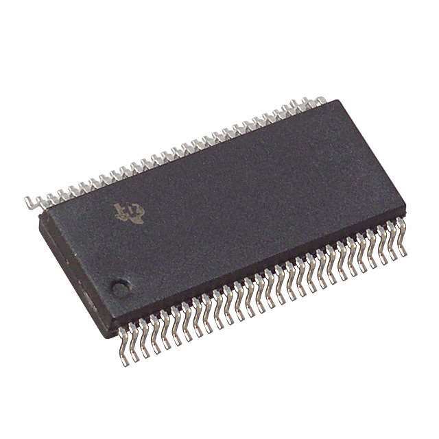
| 描述 | IC BUS TRANSCVR 16BIT 56SSOP总线收发器 Tri-St. 16-Bit |
| 产品分类 | |
| 品牌 | Texas Instruments |
| 产品手册 | |
| 产品图片 |
|
| rohs | 符合RoHS无铅 / 符合限制有害物质指令(RoHS)规范要求 |
| 产品系列 | 逻辑集成电路,总线收发器,Texas Instruments SN74ABT16652DLR74ABT |
| 数据手册 | |
| 产品型号 | SN74ABT16652DLR |
| 产品目录页面 | |
| 产品种类 | 总线收发器 |
| 传播延迟时间 | 4.1 ns |
| 低电平输出电流 | 64 mA |
| 供应商器件封装 | 56-SSOP |
| 元件数 | 2 |
| 其它名称 | 296-14657-1 |
| 功能 | Bus Transceiver / Register |
| 包装 | 剪切带 (CT) |
| 单位重量 | 694.800 mg |
| 商标 | Texas Instruments |
| 安装类型 | 表面贴装 |
| 安装风格 | SMD/SMT |
| 封装 | Reel |
| 封装/外壳 | 56-BSSOP(0.295",7.50mm 宽) |
| 封装/箱体 | SSOP-56 |
| 工作温度 | -40°C ~ 85°C |
| 工厂包装数量 | 1000 |
| 最大工作温度 | + 85 C |
| 最小工作温度 | - 40 C |
| 极性 | Non-Inverting |
| 标准包装 | 1 |
| 每元件位数 | 8 |
| 每芯片的通道数量 | 16 |
| 电压-电源 | 4.5 V ~ 5.5 V |
| 电流-输出高,低 | 32mA,64mA |
| 电源电压-最大 | 5.5 V |
| 电源电压-最小 | 4.5 V |
| 电路数量 | 2 |
| 系列 | SN74ABT16652 |
| 输入电平 | TTL |
| 输出电平 | TTL |
| 输出类型 | 3-State |
| 逻辑类型 | 寄存收发器,非反相 |
| 逻辑系列 | ABT |
| 高电平输出电流 | - 32 mA |


- 商务部:美国ITC正式对集成电路等产品启动337调查
- 曝三星4nm工艺存在良率问题 高通将骁龙8 Gen1或转产台积电
- 太阳诱电将投资9.5亿元在常州建新厂生产MLCC 预计2023年完工
- 英特尔发布欧洲新工厂建设计划 深化IDM 2.0 战略
- 台积电先进制程称霸业界 有大客户加持明年业绩稳了
- 达到5530亿美元!SIA预计今年全球半导体销售额将创下新高
- 英特尔拟将自动驾驶子公司Mobileye上市 估值或超500亿美元
- 三星加码芯片和SET,合并消费电子和移动部门,撤换高东真等 CEO
- 三星电子宣布重大人事变动 还合并消费电子和移动部门
- 海关总署:前11个月进口集成电路产品价值2.52万亿元 增长14.8%


PDF Datasheet 数据手册内容提取
SN54ABT16652, SN74ABT16652 16-BIT BUS TRANSCEIVERS AND REGISTERS WITH 3-STATE OUTPUTS SCBS215B – FEBRUARY 1991 – REVISED JANUARY 1997 (cid:1) Members of the Texas Instruments SN54ABT16652...WD PACKAGE Widebus Family SN74ABT16652...DL PACKAGE (cid:1) (TOP VIEW) State-of-the-Art EPIC-II B BiCMOS Design Significantly Reduces Power Dissipation 1OEAB 1 56 1OEBA (cid:1) Latch-Up Performance Exceeds 500 mA Per 1CLKAB 2 55 1CLKBA JEDEC Standard JESD-17 1SAB 3 54 1SBA (cid:1) Typical V (Output Ground Bounce) GND 4 53 GND OLP < 1 V at V = 5 V, T = 25°C 1A1 5 52 1B1 CC A (cid:1) 1A2 6 51 1B2 Distributed V and GND Pin Configuration CC Minimizes High-Speed Switching Noise VCC 7 50 VCC (cid:1) 1A3 8 49 1B3 Flow-Through Architecture Optimizes PCB 1A4 9 48 1B4 Layout 1A5 10 47 1B5 (cid:1) High-Drive Outputs (–32-mA IOH, 64-mA IOL) GND 11 46 GND (cid:1) Package Options Include Plastic 300-mil 1A6 12 45 1B6 Shrink Small-Outline (DL) Package and 1A7 13 44 1B7 380-mil Fine-Pitch Ceramic Flat (WD) 1A8 14 43 1B8 Package Using 25-mil Center-to-Center 2A1 15 42 2B1 Spacings 2A2 16 41 2B2 2A3 17 40 2B3 description GND 18 39 GND 2A4 19 38 2B4 The ’ABT16652 are 16-bit bus transceivers that 2A5 20 37 2B5 consist of D-type flip-flops and control circuitry 2A6 21 36 2B6 arranged for multiplexed transmission of data directly from the data bus or from the internal VCC 22 35 VCC 2A7 23 34 2B7 storage registers. These devices can be used as two 8-bit transceivers or one 16-bit transceiver. 2A8 24 33 2B8 GND 25 32 GND Output-enable (OEAB and OEBA) inputs are 2SAB 26 31 2SBA provided to control the transceiver functions. 2CLKAB 27 30 2CLKBA Select-control (SAB and SBA) inputs are provided 2OEAB 28 29 2OEBA to select whether real-time or stored data is transferred. The circuitry used for select control eliminates the typical decoding glitch that occurs in a multiplexer during the transition between stored and real-time data. A low input selects real-time data, and a high input selects stored data. Figure 1 illustrates the four fundamental bus-management functions that can be performed with the ’ABT16652. Data on the A- or B-data bus, or both, can be stored in the internal D-type flip-flops by low-to-high transitions at the appropriate clock (CLKAB or CLKBA) inputs regardless of the select- or enable-control inputs. When SAB and SBA are in the real-time transfer mode, it is possible to store data without using the internal D-type flip-flops by simultaneously enabling OEAB and OEBA. In this configuration, each output reinforces its input. When all other data sources to the two sets of bus lines are at high impedance, each set of bus lines remains at its last state. Please be aware that an important notice concerning availability, standard warranty, and use in critical applications of TexasInstruments semiconductor products and disclaimers thereto appears at the end of this data sheet. Widebus and EPIC-II B are trademarks of Texas Instruments Incorporated. PRODUCTION DATA information is current as of publication date. Copyright 1997, Texas Instruments Incorporated Products conform to specifications per the terms of Texas Instruments standard warranty. Production processing does not necessarily include testing of all parameters. POST OFFICE BOX 655303 • DALLAS, TEXAS 75265 1
SN54ABT16652, SN74ABT16652 16-BIT BUS TRANSCEIVERS AND REGISTERS WITH 3-STATE OUTPUTS SCBS215B – FEBRUARY 1991 – REVISED JANUARY 1997 description (continued) To ensure the high-impedance state during power up or power down, OEBA should be tied to V through a CC pullup resistor; the minimum value of the resistor is determined by the current-sinking capability of the driver (B to A). OEAB should be tied to GND through a pulldown resistor; the minimum value of the resistor is determined by the current-sourcing capability of the driver (A to B). The SN54ABT16652 is characterized for operation over the full military temperature range of –55°C to 125°C. The SN74ABT16652 is characterized for operation from –40°C to 85°C. FUNCTION TABLE INPUTS DATA I/O† OOPPEERRAATTIIOONN OORR FFUUNNCCTTIIOONN OEAB OEBA CLKAB CLKBA SAB SBA A1–A8 B1–B8 L H H or L H or L X X Input Input Isolation L H ↑ ↑ X X Input Input Store A and B data X H ↑ H or L X X Input Unspecified‡ Store A, hold B H H ↑ ↑ X‡ X Input Output Store A in both registers L X H or L ↑ X X Unspecified‡ Input Hold A, store B L L ↑ ↑ X X‡ Output Input Store B in both registers L L X X X L Output Input Real-time B data to A bus L L X H or L X H Output Input Stored B data to A bus H H X X L X Input Output Real-time A data to B bus H H H or L X H X Input Output Stored A data to B bus Stored A data to B bus and H L H or L H or L H H Output Output stored B data to A bus †The data-output functions may be enabled or disabled by a variety of level combinations at OEAB or OEBA. Data-input functions are always enabled; i.e., data at the bus terminals is stored on every low-to-high transition of the clock inputs. ‡Select control = L; clocks can occur simultaneously. Select control = H; clocks must be staggered to load both registers. 2 POST OFFICE BOX 655303 • DALLAS, TEXAS 75265
SN54ABT16652, SN74ABT16652 16-BIT BUS TRANSCEIVERS AND REGISTERS WITH 3-STATE OUTPUTS SCBS215B – FEBRUARY 1991 – REVISED JANUARY 1997 A B A B S S S S U U U U B B B B OEAB OEBA CLKAB CLKBA SAB SBA OEAB OEBA CLKAB CLKBA SAB SBA L L X X X L H H X X L X REAL-TIME TRANSFER REAL-TIME TRANSFER BUS B TO BUS A BUS A TO BUS B A B A B S S S S U U U U B B B B OEAB OEBA CLKAB CLKBA SAB SBA OEAB OEBA CLKAB CLKBA SAB SBA X H ↑ X X X H L H or L H or L H H L X X ↑ X X L H ↑ ↑ X X STORAGE FROM TRANSFER STORED DATA A, B, OR A AND B TO A AND/OR B Figure 1. Bus-Management Functions POST OFFICE BOX 655303 • DALLAS, TEXAS 75265 3
SN54ABT16652, SN74ABT16652 16-BIT BUS TRANSCEIVERS AND REGISTERS WITH 3-STATE OUTPUTS SCBS215B – FEBRUARY 1991 – REVISED JANUARY 1997 logic symbol† 56 1OEBA EN1 [BA] 1 1OEAB EN2 [AB] 55 1CLKBA C3 54 1SBA G4 2 1CLKAB C5 3 1SAB G6 29 2OEBA EN7 [BA] 28 2OEAB EN8 [AB] 30 2CLKBA C9 31 2SBA G10 27 2CLKAB C11 26 2SAB G12 52 5 ≥1 4 3D 1B1 1A1 1 4 1 5D 6 ≥1 2 1 6 6 51 1A2 1B2 8 49 1A3 1B3 9 48 1A4 1B4 10 47 1A5 1B5 12 45 1A6 1B6 13 44 1A7 1B7 14 43 1A8 1B8 15 ≥1 10 9D 42 2B1 2A1 7 10 1 11D 12 ≥1 8 1 12 16 41 2A2 2B2 17 40 2A3 2B3 19 38 2A4 2B4 20 37 2A5 2B5 21 36 2A6 2B6 23 34 2A7 2B7 24 33 2A8 2B8 †This symbol is in accordance with ANSI/IEEE Std 91-1984 and IEC Publication 617-12. 4 POST OFFICE BOX 655303 • DALLAS, TEXAS 75265
SN54ABT16652, SN74ABT16652 16-BIT BUS TRANSCEIVERS AND REGISTERS WITH 3-STATE OUTPUTS SCBS215B – FEBRUARY 1991 – REVISED JANUARY 1997 logic diagram (positive logic) 56 1OEBA 1 1OEAB 55 1CLKBA 54 1SBA 2 1CLKAB 3 1SAB One of Eight Channels 1D C1 5 1A1 52 1B1 1D C1 To Seven Other Channels 29 2OEBA 28 2OEAB 30 2CLKBA 31 2SBA 27 2CLKAB 26 2SAB One of Eight Channels 1D C1 15 2A1 42 2B1 1D C1 To Seven Other Channels POST OFFICE BOX 655303 • DALLAS, TEXAS 75265 5
SN54ABT16652, SN74ABT16652 16-BIT BUS TRANSCEIVERS AND REGISTERS WITH 3-STATE OUTPUTS SCBS215B – FEBRUARY 1991 – REVISED JANUARY 1997 absolute maximum ratings over operating free-air temperature range (unless otherwise noted)† Supply voltage range, V . . . . . . . . . . . . . . . . . . . . . . . . . . . . . . . . . . . . . . . . . . . . . . . . . . . . . . . . . . –0.5 V to 7 V CC Input voltage range, V (except I/O ports) (see Note 1) . . . . . . . . . . . . . . . . . . . . . . . . . . . . . . . . . . –0.5 V to 7 V I Voltage range applied to any output in the high or power-off state, V . . . . . . . . . . . . . . . . . . . –0.5 V to 5.5 V O Current into any output in the low state, I : SN54ABT16652 . . . . . . . . . . . . . . . . . . . . . . . . . . . . . . . . . . 96 mA O SN74ABT16652 . . . . . . . . . . . . . . . . . . . . . . . . . . . . . . . . . 128 mA Input clamp current, I (V < 0) . . . . . . . . . . . . . . . . . . . . . . . . . . . . . . . . . . . . . . . . . . . . . . . . . . . . . . . . . . . –18 mA IK I Output clamp current, I (V < 0) . . . . . . . . . . . . . . . . . . . . . . . . . . . . . . . . . . . . . . . . . . . . . . . . . . . . . . . . –50 mA OK O Package thermal impedance, q JA (see Note 2): DL package . . . . . . . . . . . . . . . . . . . . . . . . . . . . . . . . . . 74°C/W Storage temperature range, T . . . . . . . . . . . . . . . . . . . . . . . . . . . . . . . . . . . . . . . . . . . . . . . . . . . –65°C to 150°C stg †Stresses beyond those listed under “absolute maximum ratings” may cause permanent damage to the device. These are stress ratings only, and functional operation of the device at these or any other conditions beyond those indicated under “recommended operating conditions” is not implied. Exposure to absolute-maximum-rated conditions for extended periods may affect device reliability. NOTES: 1. The input and output negative-voltage ratings may be exceeded if the input and output clamp-current ratings are observed. 2. The package thermal impedance is calculated in accordance with EIA/JEDEC Std JESD51. recommended operating conditions (see Note 3) SN54ABT16652 SN74ABT16652 UUNNIITT MIN MAX MIN MAX VCC Supply voltage 4.5 5.5 4.5 5.5 V VIH High-level input voltage 2 2 V VIL Low-level input voltage 0.8 0.8 V VI Input voltage 0 VCC 0 VCC V IOH High-level output current –24 –32 mA IOL Low-level output current 48 64 mA D t/D v Input transition rise or fall rate Outputs enabled 10 10 ns/V TA Operating free-air temperature –55 125 –40 85 °C NOTE 3: Unused pins (input or I/O) must be held high or low to prevent them from floating. 6 POST OFFICE BOX 655303 • DALLAS, TEXAS 75265
SN54ABT16652, SN74ABT16652 16-BIT BUS TRANSCEIVERS AND REGISTERS WITH 3-STATE OUTPUTS SCBS215B – FEBRUARY 1991 – REVISED JANUARY 1997 electrical characteristics over recommended operating free-air temperature range (unless otherwise noted) TA = 25°C SN54ABT16652 SN74ABT16652 PPAARRAAMMEETTEERR TTEESSTT CCOONNDDIITTIIOONNSS UUNNIITT MIN TYP† MAX MIN MAX MIN MAX VIK VCC = 4.5 V, II = –18 mA –1.2 –1.2 –1.2 V VCC = 4.5 V, IOH = –3 mA 2.5 2.5 2.5 VCC = 5 V, IOH = –3 mA 3 3 3 VVOOHH VV IOH = –24 mA 2 2 VVCCCC == 44.55 VV IOH = –32 mA 2* 2 IOL = 48 mA 0.55 0.55 VVOOLL VVCCCC == 44.55 VV VV IOL = 64 mA 0.55* 0.55 Vhys 100 mV Control ±1 ±1 ±1 III inputs VCCCC = 5.5 V,, VII = VCCCC or GND mm A A or B ports ±20 ±20 ±20 IOZH‡ VCC = 5.5 V, VO = 2.7 V 10 10 10 m A IOZL‡ VCC = 5.5 V, VO = 0.5 V –10 –10 –10 m A Ioff VCC = 0, VI or VO ≤ 4.5 V ±100 ±100 m A ICEX VVCOC = =5 .55. 5V V, Outputs high 50 50 50 m A IO§ VCC = 5.5 V, VO = 2.5 V –50 –100 –180 –50 –180 –50 –180 mA Outputs high 2 2 2 VVCCCC == 55..55 VV,, ICC A or B ports IO = 0, Outputs low 32 32 32 mA VI = VCC or GND Outputs disabled 2 2 2 VCC = 5.5 V, Outputs enabled 50 50 50 One input at 3.4 V,, DDaattaa iinnppuuttss Other inputs at D ICC¶¶ VCC or GND Outputs disabled 50 50 50 m A Control VCC = 5.5 V, One input at 3.4 V, 50 50 50 inputs Other inputs at VCC or GND Control Ci inputs VI = 2.5 V or 0.5 V 4 pF Cio A or B ports VO = 2.5 V or 0.5 V 8 pF * On products compliant to MIL-PRF-38535, this parameter does not apply. †All typical values are at VCC = 5 V. ‡The parameters IOZH and IOZL include the input leakage current. §Not more than one output should be tested at a time, and the duration of the test should not exceed one second. ¶This is the increase in supply current for each input that is at the specified TTL voltage level rather than VCC or GND. POST OFFICE BOX 655303 • DALLAS, TEXAS 75265 7
SN54ABT16652, SN74ABT16652 16-BIT BUS TRANSCEIVERS AND REGISTERS WITH 3-STATE OUTPUTS SCBS215B – FEBRUARY 1991 – REVISED JANUARY 1997 timing requirements over recommended ranges of supply voltage and operating free-air temperature (unless otherwise noted) (see Figure 2) SN54ABT16652 VCC = 5 V, TA = 25°C MIN MAX UNIT MIN MAX fclock Clock frequency 0 125 0 125 MHz tw Pulse duration, CLK high or low 4.3 4.3 ns tsu Setup time, A or B before CLKAB↑ or CLKBA↑ 3.5 4 ns th Hold time, A or B after CLKAB↑ or CLKBA↑ 0.5 0.5 ns timing requirements over recommended ranges of supply voltage and operating free-air temperature (unless otherwise noted) (see Figure 2) SN74ABT16652 VCC = 5 V, TA = 25°C MIN MAX UNIT MIN MAX fclock Clock frequency 0 125 0 125 MHz tw Pulse duration, CLK high or low 4.3 4.3 ns tsu Setup time, A or B before CLKAB↑ or CLKBA↑ 3 3 ns th Hold time, A or B after CLKAB↑ or CLKBA↑ 0 0 ns 8 POST OFFICE BOX 655303 • DALLAS, TEXAS 75265
SN54ABT16652, SN74ABT16652 16-BIT BUS TRANSCEIVERS AND REGISTERS WITH 3-STATE OUTPUTS SCBS215B – FEBRUARY 1991 – REVISED JANUARY 1997 switching characteristics over recommended ranges of supply voltage and operating free-air temperature, C = 50 pF (unless otherwise noted) (see Figure 2) L SN54ABT16652 FROM TO VCC = 5 V, PARAMETER (INPUT) (OUTPUT) TA = 25°C MIN MAX UNIT MIN TYP MAX fmax 125 125 MHz tPLH 1.5 3.1 4 1 5 CCLLKK BB oorr AA nnss tPHL 1.5 3.2 4.1 1 5 tPLH 1 2.3 3.2 0.6 4 AA oorr BB BB oorr AA nnss tPHL 1 3 4.1 0.6 4.9 tPLH 1 2.9 4.3 0.6 5.3 SSAABB oorr SSBBAA†† BB oorr AA nnss tPHL 1 3.1 4.6 0.6 5.3 tPZH 1 2.8 4.1 0.6 5.2 OOEEBBAA AA nnss tPZL 1.5 3.1 4.4 1 5.4 tPHZ 1.5 3.4 4.7 0.8 5.3 OOEEBBAA AA nnss tPLZ 1.5 2.7 4 1 5.3 tPZH 1 2.6 3.6 0.8 4.7 OOEEAABB BB nnss tPZL 1.5 2.8 4.5 1 5 tPHZ 2 4.2 5.9 1 6.4 OOEEAABB BB nnss tPLZ 1.5 3.4 4.9 1 5.9 †These parameters are measured with the internal output state of the storage register opposite that of the bus input. switching characteristics over recommended ranges of supply voltage and operating free-air temperature, C = 50 pF (unless otherwise noted) (see Figure 2) L SN74ABT16652 FROM TO VCC = 5 V, PARAMETER (INPUT) (OUTPUT) TA = 25°C MIN MAX UNIT MIN TYP MAX fmax 125 125 MHz tPLH 1.5 3.1 4 1.5 4.9 CCLLKK BB oorr AA nnss tPHL 1.5 3.2 4.1 1.5 4.7 tPLH 1 2.3 3.2 1 3.9 AA oorr BB BB oorr AA nnss tPHL 1 3 4.1 1 4.6 tPLH 1 2.9 4.3 1 5 SSAABB oorr SSBBAA†† BB oorr AA nnss tPHL 1 3.1 4.3 1 5 tPZH 1 2.8 4.1 1 5 OOEEBBAA AA nnss tPZL 1.5 3.1 4.4 1.5 5.3 tPHZ 1.5 3.4 4.4 1.5 4.9 OOEEBBAA AA nnss tPLZ 1.5 2.7 3.6 1.5 4 tPZH 1 2.6 3.6 1 4.2 OOEEAABB BB nnss tPZL 1.5 2.8 3.9 1.5 4.6 tPHZ 2 4.2 5.5 2 5.9 OOEEAABB BB nnss tPLZ 1.5 3.4 4.5 1.5 5.2 †These parameters are measured with the internal output state of the storage register opposite that of the bus input. POST OFFICE BOX 655303 • DALLAS, TEXAS 75265 9
SN54ABT16652, SN74ABT16652 16-BIT BUS TRANSCEIVERS AND REGISTERS WITH 3-STATE OUTPUTS SCBS215B – FEBRUARY 1991 – REVISED JANUARY 1997 PARAMETER MEASUREMENT INFORMATION 7 V TEST S1 500 W S1 Open From Output tPLH/tPHL Open Under Test GND tPLZ/tPZL 7 V CL = 50 pF 500 W tPHZ/tPZH Open (see Note A) 3 V LOAD CIRCUIT Timing Input 1.5 V 0 V tw tsu th 3 V 3 V Input 1.5 V 1.5 V Data Input 1.5 V 1.5 V 0 V 0 V VOLTAGE WAVEFORMS VOLTAGE WAVEFORMS PULSE DURATION SETUP AND HOLD TIMES 3 V 3 V OOuuttppuutt Input 1.5 V 1.5 V 1.5 V 1.5 V CCoonnttrrooll 0 V 0 V tPZL tPLH tPHL VOH Output tPLZ 3.5 V Output 1.5 V 1.5 V VOL WavSe1f oatr m7 V1 1.5 V VOL + 0.3 V VOL (see Note B) tPHZ tPHL tPLH tPZH Output VOH VOH Output 1.5 V 1.5 V WSa1v aetf oOrpme n2 1.5 V VOH – 0.3 V VOL (see Note B) ≈ 0 V VOLTAGE WAVEFORMS VOLTAGE WAVEFORMS PROPAGATION DELAY TIMES ENABLE AND DISABLE TIMES INVERTING AND NONINVERTING OUTPUTS LOW- AND HIGH-LEVEL ENABLING NOTES: A. CL includes probe and jig capacitance. B. Waveform 1 is for an output with internal conditions such that the output is low except when disabled by the output control. Waveform2 is for an output with internal conditions such that the output is high except when disabled by the output control. C. All input pulses are supplied by generators having the following characteristics: PRR ≤ 10 MHz, ZO = 50 W , tr ≤ 2.5 ns, tf≤ 2.5 ns. D. The outputs are measured one at a time with one transition per measurement. Figure 2. Load Circuit and Voltage Waveforms 10 POST OFFICE BOX 655303 • DALLAS, TEXAS 75265
PACKAGE OPTION ADDENDUM www.ti.com 6-Feb-2020 PACKAGING INFORMATION Orderable Device Status Package Type Package Pins Package Eco Plan Lead/Ball Finish MSL Peak Temp Op Temp (°C) Device Marking Samples (1) Drawing Qty (2) (6) (3) (4/5) SN74ABT16652DL ACTIVE SSOP DL 56 20 Green (RoHS NIPDAU Level-1-260C-UNLIM -40 to 85 ABT16652 & no Sb/Br) SN74ABT16652DLR ACTIVE SSOP DL 56 1000 Green (RoHS NIPDAU Level-1-260C-UNLIM -40 to 85 ABT16652 & no Sb/Br) (1) The marketing status values are defined as follows: ACTIVE: Product device recommended for new designs. LIFEBUY: TI has announced that the device will be discontinued, and a lifetime-buy period is in effect. NRND: Not recommended for new designs. Device is in production to support existing customers, but TI does not recommend using this part in a new design. PREVIEW: Device has been announced but is not in production. Samples may or may not be available. OBSOLETE: TI has discontinued the production of the device. (2) RoHS: TI defines "RoHS" to mean semiconductor products that are compliant with the current EU RoHS requirements for all 10 RoHS substances, including the requirement that RoHS substance do not exceed 0.1% by weight in homogeneous materials. Where designed to be soldered at high temperatures, "RoHS" products are suitable for use in specified lead-free processes. TI may reference these types of products as "Pb-Free". RoHS Exempt: TI defines "RoHS Exempt" to mean products that contain lead but are compliant with EU RoHS pursuant to a specific EU RoHS exemption. Green: TI defines "Green" to mean the content of Chlorine (Cl) and Bromine (Br) based flame retardants meet JS709B low halogen requirements of <=1000ppm threshold. Antimony trioxide based flame retardants must also meet the <=1000ppm threshold requirement. (3) MSL, Peak Temp. - The Moisture Sensitivity Level rating according to the JEDEC industry standard classifications, and peak solder temperature. (4) There may be additional marking, which relates to the logo, the lot trace code information, or the environmental category on the device. (5) Multiple Device Markings will be inside parentheses. Only one Device Marking contained in parentheses and separated by a "~" will appear on a device. If a line is indented then it is a continuation of the previous line and the two combined represent the entire Device Marking for that device. (6) Lead/Ball Finish - Orderable Devices may have multiple material finish options. Finish options are separated by a vertical ruled line. Lead/Ball Finish values may wrap to two lines if the finish value exceeds the maximum column width. Important Information and Disclaimer:The information provided on this page represents TI's knowledge and belief as of the date that it is provided. TI bases its knowledge and belief on information provided by third parties, and makes no representation or warranty as to the accuracy of such information. Efforts are underway to better integrate information from third parties. TI has taken and continues to take reasonable steps to provide representative and accurate information but may not have conducted destructive testing or chemical analysis on incoming materials and chemicals. TI and TI suppliers consider certain information to be proprietary, and thus CAS numbers and other limited information may not be available for release. In no event shall TI's liability arising out of such information exceed the total purchase price of the TI part(s) at issue in this document sold by TI to Customer on an annual basis. Addendum-Page 1
PACKAGE OPTION ADDENDUM www.ti.com 6-Feb-2020 Addendum-Page 2
PACKAGE MATERIALS INFORMATION www.ti.com 14-Jul-2012 TAPE AND REEL INFORMATION *Alldimensionsarenominal Device Package Package Pins SPQ Reel Reel A0 B0 K0 P1 W Pin1 Type Drawing Diameter Width (mm) (mm) (mm) (mm) (mm) Quadrant (mm) W1(mm) SN74ABT16652DLR SSOP DL 56 1000 330.0 32.4 11.35 18.67 3.1 16.0 32.0 Q1 PackMaterials-Page1
PACKAGE MATERIALS INFORMATION www.ti.com 14-Jul-2012 *Alldimensionsarenominal Device PackageType PackageDrawing Pins SPQ Length(mm) Width(mm) Height(mm) SN74ABT16652DLR SSOP DL 56 1000 367.0 367.0 55.0 PackMaterials-Page2
None
IMPORTANTNOTICEANDDISCLAIMER TI PROVIDES TECHNICAL AND RELIABILITY DATA (INCLUDING DATASHEETS), DESIGN RESOURCES (INCLUDING REFERENCE DESIGNS), APPLICATION OR OTHER DESIGN ADVICE, WEB TOOLS, SAFETY INFORMATION, AND OTHER RESOURCES “AS IS” AND WITH ALL FAULTS, AND DISCLAIMS ALL WARRANTIES, EXPRESS AND IMPLIED, INCLUDING WITHOUT LIMITATION ANY IMPLIED WARRANTIES OF MERCHANTABILITY, FITNESS FOR A PARTICULAR PURPOSE OR NON-INFRINGEMENT OF THIRD PARTY INTELLECTUAL PROPERTY RIGHTS. These resources are intended for skilled developers designing with TI products. You are solely responsible for (1) selecting the appropriate TI products for your application, (2) designing, validating and testing your application, and (3) ensuring your application meets applicable standards, and any other safety, security, or other requirements. These resources are subject to change without notice. TI grants you permission to use these resources only for development of an application that uses the TI products described in the resource. Other reproduction and display of these resources is prohibited. No license is granted to any other TI intellectual property right or to any third party intellectual property right. TI disclaims responsibility for, and you will fully indemnify TI and its representatives against, any claims, damages, costs, losses, and liabilities arising out of your use of these resources. TI’s products are provided subject to TI’s Terms of Sale (www.ti.com/legal/termsofsale.html) or other applicable terms available either on ti.com or provided in conjunction with such TI products. TI’s provision of these resources does not expand or otherwise alter TI’s applicable warranties or warranty disclaimers for TI products. Mailing Address: Texas Instruments, Post Office Box 655303, Dallas, Texas 75265 Copyright © 2020, Texas Instruments Incorporated