ICGOO在线商城 > 集成电路(IC) > 接口 - 串行器,解串行器 > SN65LV1023ARHBT
- 型号: SN65LV1023ARHBT
- 制造商: Texas Instruments
- 库位|库存: xxxx|xxxx
- 要求:
| 数量阶梯 | 香港交货 | 国内含税 |
| +xxxx | $xxxx | ¥xxxx |
查看当月历史价格
查看今年历史价格
SN65LV1023ARHBT产品简介:
ICGOO电子元器件商城为您提供SN65LV1023ARHBT由Texas Instruments设计生产,在icgoo商城现货销售,并且可以通过原厂、代理商等渠道进行代购。 SN65LV1023ARHBT价格参考¥30.52-¥56.96。Texas InstrumentsSN65LV1023ARHBT封装/规格:接口 - 串行器,解串行器, 660Mbps Serializer 10 Input 1 Output 32-VQFN (5x5)。您可以下载SN65LV1023ARHBT参考资料、Datasheet数据手册功能说明书,资料中有SN65LV1023ARHBT 详细功能的应用电路图电压和使用方法及教程。
SN65LV1023ARHBT 是 Texas Instruments(德州仪器)生产的一款接口芯片,属于串行器/解串化器(Serializer/Deserializer, SerDes)类别。它主要用于高速数据传输和信号转换,广泛应用于工业、通信和消费电子领域。以下是该型号的一些典型应用场景:

 1. 工业自动化
   - 在工业控制系统中,SN65LV1023ARHBT 可用于实现长距离、低延迟的数据传输,例如在可编程逻辑控制器(PLC)与传感器或执行器之间的通信。
   - 它支持 LVDS(低压差分信号)技术,能够减少电磁干扰(EMI),适合高噪声环境下的稳定数据传输。

 2. 视频和显示系统
   - 该芯片可用于视频信号的串行化和解串化,特别是在需要将多条并行数据线转换为单条高速差分信号的应用中,如 LCD 显示屏或摄像头模块的数据传输。
   - 它能够满足高清分辨率和实时性要求,适用于监控摄像头、医疗成像设备等。

 3. 通信设备
   - SN65LV1023ARHBT 常用于路由器、交换机和其他网络设备中的背板通信,以实现高效的信号传输。
   - 其低功耗特性和高可靠性使其非常适合对性能和能耗有严格要求的通信基础设施。

 4. 汽车电子
   - 在汽车行业中,这款芯片可以用于车载信息娱乐系统、高级驾驶辅助系统(ADAS)以及仪表盘显示模块的数据传输。
   - 它支持长距离传输能力,能够在复杂的车内环境中提供稳定的信号连接。

 5. 消费电子产品
   - 该芯片适用于需要高速数据接口的消费类设备,如数码相机、打印机和游戏机。
   - 它的紧凑封装形式和低功耗设计非常适合便携式设备。

 核心优势
- 高速传输:支持高达 655 Mbps 的数据速率。
- 低功耗:优化了电源管理,适合电池供电设备。
- 抗干扰能力强:采用 LVDS 技术,降低了信号损耗和噪声影响。
- 灵活性:支持多种输入输出配置,便于集成到不同系统中。

总之,SN65LV1023ARHBT 是一款功能强大的串行器/解串化器芯片,适用于需要高效、可靠数据传输的各种场景。
| 参数 | 数值 |
| 产品目录 | 集成电路 (IC)半导体 |
| 描述 | IC SERIAL/DESERIAL 10:1 32-VQFNLVDS 接口集成电路 10:1 LVDS Serdes Trnsmtr 100-660Mbps |
| 产品分类 | |
| 品牌 | Texas Instruments |
| 产品手册 | |
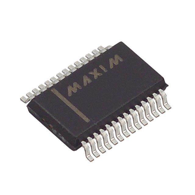
| 产品图片 |
|
| rohs | 符合RoHS无铅 / 符合限制有害物质指令(RoHS)规范要求 |
| 产品系列 | 接口 IC,LVDS 接口集成电路,Texas Instruments SN65LV1023ARHBT65LV |
| 数据手册 | |
| 产品型号 | SN65LV1023ARHBT |
| 产品种类 | LVDS 接口集成电路 |
| 供应商器件封装 | 32-VQFN(5x5) |
| 其它名称 | 296-27993-6 |
| 功能 | 串行器 |
| 包装 | Digi-Reel® |
| 单位重量 | 71.800 mg |
| 商标 | Texas Instruments |
| 安装类型 | 表面贴装 |
| 安装风格 | SMD/SMT |
| 封装 | Reel |
| 封装/外壳 | 32-VFQFN 裸露焊盘 |
| 封装/箱体 | VQFN-32 |
| 工作温度 | -40°C ~ 85°C |
| 工作电源电压 | 3.3 V |
| 工厂包装数量 | 250 |
| 接收机数量 | 10 |
| 数据速率 | 660Mbps |
| 最大工作温度 | + 85 C |
| 最小工作温度 | - 40 C |
| 标准包装 | 1 |
| 激励器数量 | 1 |
| 电压-电源 | 3 V ~ 3.6 V |
| 电源电压-最大 | 3.6 V |
| 电源电压-最小 | 3 V |
| 类型 | LVDS |
| 系列 | SN65LV1023A |
| 输入数 | 10 |
| 输入类型 | LVTTL |
| 输出数 | 1 |
| 输出类型 | LVDS |





- 商务部:美国ITC正式对集成电路等产品启动337调查
- 曝三星4nm工艺存在良率问题 高通将骁龙8 Gen1或转产台积电
- 太阳诱电将投资9.5亿元在常州建新厂生产MLCC 预计2023年完工
- 英特尔发布欧洲新工厂建设计划 深化IDM 2.0 战略
- 台积电先进制程称霸业界 有大客户加持明年业绩稳了
- 达到5530亿美元!SIA预计今年全球半导体销售额将创下新高
- 英特尔拟将自动驾驶子公司Mobileye上市 估值或超500亿美元
- 三星加码芯片和SET,合并消费电子和移动部门,撤换高东真等 CEO
- 三星电子宣布重大人事变动 还合并消费电子和移动部门
- 海关总署:前11个月进口集成电路产品价值2.52万亿元 增长14.8%



PDF Datasheet 数据手册内容提取
SN65LV1023A SN65LV1224B www.ti.com SLLS621E–SEPTEMBER2004–REVISEDDECEMBER2009 10-MHz To 66-MHz, 10:1 LVDS SERIALIZER/DESERIALIZER CheckforSamples:SN65LV1023ASN65LV1224B FEATURES 1 DESCRIPTION • 100-Mbpsto660-MbpsSerialLVDSData PayloadBandwidthat10-MHzto66-MHz The SN65LV1023A serializer and SN65LV1224B SystemClock deserializer comprise a 10-bit serdes chipset • Pin-CompatibleSupersetof designed to transmit and receive serial data over DS92LV1023/DS92LV1224 LVDS differential backplanes at equivalent parallel word rates from 10 MHz to 66 MHz. Including • Chipset(Serializer/Deserializer)Power overhead, this translates into a serial data rate Consumption<450mW(Typ)at66MHz between 120-Mbps and 792-Mbps payload encoded • SynchronizationModeforFasterLock throughput. • LockIndicator Upon power up, the chipset link can be initialized via • NoExternalComponentsRequiredforPLL a synchronization mode with internally generated SYNC patterns or the deserializer can be allowed to • 28-PinSSOPandSpaceSaving5× 5mmQFN synchronize to random data. By using the PackagesAvailable synchronization mode, the deserializer establishes • IndustrialTemperatureQualified, lockwithinspecified,shortertimeparameters. T =−40°Cto85°C A The device can be entered into a power-down state • ProgrammableEdgeTriggeronClock when no data transfer is required. Alternatively, a • Flow-ThroughPinoutforEasyPCBLayout mode is available to place the output pins in the high-impedancestatewithoutlosingPLLlock. APPLICATIONS The SN65LV1023A and SN65LV1224B are • WirelessBaseStation characterized for operation over ambient air • BackplaneInterconnect temperatureof–40°Cto85°C. • DSLAM SSYYNNCC12 12 2287 DDVVCCCC DIN0 SYNC2 SYNC1 DVCC DVCC DVCC DVCC AVCC D 3 26 AV IN0 CC D 4 25 AGND 32 31 30 29 28 27 26 25 IN1 D 5 24 PWRDN DIN1 1 24 AGND IN2 DIN3 6 23 AGND DIN2 2 23 PWRDN DB Package DIN4 7 SN65LV1023A22 DO+ DIN3 3 RHB Package 22 AGND D 8 21 D − IN5 Serializer O D 4 SN65LV1023A 21 D IN4 O+ D 9 20 AGND IN6 Serializer D 5 20 D DIN7 10 19 DEN IN5 (Top View) O− DIN8 11 18 AGND DIN6 6 19 AGND DIN9 12 17 AVCC DIN7 7 18 DEN TCLK_R/F 13 16 DGND D 8 17 AGND TCLK 14 15 DGND IN8 9 10 11 12 13 14 15 16 9 F K D D D D C DIN K_R/ TCL DGN DGN DGN DGN AVC L C T 1 Pleasebeawarethatanimportantnoticeconcerningavailability,standardwarranty,anduseincriticalapplicationsofTexas Instrumentssemiconductorproductsanddisclaimerstheretoappearsattheendofthisdatasheet. PRODUCTIONDATAinformationiscurrentasofpublicationdate. Copyright©2004–2009,TexasInstrumentsIncorporated Products conform to specifications per the terms of the Texas Instruments standard warranty. Production processing does not necessarilyincludetestingofallparameters.
SN65LV1023A SN65LV1224B SLLS621E–SEPTEMBER2004–REVISEDDECEMBER2009 www.ti.com Thesedeviceshavelimitedbuilt-inESDprotection.Theleadsshouldbeshortedtogetherorthedeviceplacedinconductivefoam duringstorageorhandlingtopreventelectrostaticdamagetotheMOSgates. BLOCKDIAGRAMS SN65LV1023A SN65LV1224B LVDS 10 10 al A+ Y+ el DIN h eri all ch DOUT TCLK_R/F Input Latc arallel-to-S A− Y− erial-to-Par Output Lat P S TCLK (10 MHz to REFCLK 66 MHz) Timing / Timing / PLL DEN PLL REN Control Control LOCK SYNC1 Clock RCLK_R/F SYNC2 Recovery RCLK (10 MHz to 66 MHz) 2 SubmitDocumentationFeedback Copyright©2004–2009,TexasInstrumentsIncorporated ProductFolderLink(s):SN65LV1023ASN65LV1224B
SN65LV1023A SN65LV1224B www.ti.com SLLS621E–SEPTEMBER2004–REVISEDDECEMBER2009 FUNCTIONAL DESCRIPTION The SN65LV1023A and SN65LV1224B are a 10-bit serializer/deserializer chipset designed to transmit data over differential backplanes or unshielded twisted pair (UTP) at clock speeds from 10 MHz to 66 MHz. The chipset has five states of operation: initialization mode, synchronization mode, data transmission mode, power-down mode,andhigh-impedancemode.Thefollowingsectionsdescribeeachstateofoperation. INITIALIZATION MODE Initialization of both devices must occur before data transmission can commence. Initialization refers to synchronizationoftheserializeranddeserializerPLLstolocalclocks. When V is applied to the serializer and/or deserializer, the respective outputs enter the high-impedance state, CC while on-chip power-on circuitry disables internal circuitry. When V reaches 2.45 V, the PLL in each device CC begins locking to a local clock. For the serializer, the local clock is the transmit clock (TCLK) provided by an external source. For the deserializer, a local clock must be applied to the REFCLK pin. The serializer outputs remaininthehigh-impedancestate,whilethePLLlockstotheTCLK. SYNCHRONIZATION MODE The deserializer PLL must synchronize to the serializer in order to receive valid data. Synchronization can be accomplishedinoneoftwoways: • Rapid Synchronization: The serializer has the capability to send specific SYNC patterns consisting of six ones and six zeros switching at the input clock rate. The transmission of SYNC patterns enables the deserializer to lock to the serializer signal within a deterministic time frame. This transmission of SYNC patterns is selected via the SYNC1 and SYNC2 inputs on the serializer. Upon receiving valid SYNC1 or SYNC2pulse(widerthan6clockcycles),1026cyclesofSYNCpatternaresent. When the deserializer detects edge transitions at the LVDS input, it attempts to lock to the embedded clock information. The deserializer LOCK output remains high while its PLL locks to the incoming data or SYNC patterns present on the serial input. When the deserializer locks to the LVDS data, the LOCK output goes low. When LOCK is low, the deserializer outputs represent incoming LVDS data. One approach is to tie the deserializerLOCKoutputdirectlytoSYNC1orSYNC2. • Random-Lock Synchronization: The deserializer can attain lock to a data stream without requiring the serializer to send special SYNC patterns. This allows the SN65LV1224B to operate in open-loop applications. Equally important is the deserializer’s ability to support hot insertion into a running backplane. In the open-loop or hot-insertion case, it is assumed the data stream is essentially random. Therefore, because lock timevariesduetodatastreamcharacteristics,theexactlocktimecannotbepredicted.Theprimaryconstraint on the random lock time is the initial phase relation between the incoming data and the REFCLK when the deserializerpowersup. The data contained in the data stream can also affect lock time. If a specific pattern is repetitive, the deserializer could enter false lock—falsely recognizing the data pattern as the start/stop bits. This is referred to as repetitive multitransition(RMT);seeFigure1forRMTexamples.Thisoccurswhenmorethanonelow-hightransitiontakes place per clock cycle over multiple cycles. In the worst case, the deserializer could become locked to the data pattern rather than the clock. Circuitry within the deserializer can detect that the possibility of false lock exists. Upon detection, the circuitry prevents the LOCK output from becoming active until the potential false lock pattern changes. Notice that the RMT pattern only affects the deserializer lock time, and once the deserializer is in lock, the RMT pattern does not affect the deserializer state as long as the same data boundary happens each cycle. The deserializer does not go into lock until it finds a unique four consecutive cycles of data boundary (stop/start bits)atthesameposition. The deserializer stays in lock until it cannot detect the same data boundary (stop/start bits) for four consecutive cycles. Then the deserializer goes out of lock and hunts for the new data boundary (stop/start bits). In the event of loss of synchronization, the LOCK pin output goes high and the outputs (including RCLK) enter a high-impedance state. The user’s system should monitor the LOCK pin in order to detect a loss of synchronization. Upon detection of loss of lock, sending sync patterns for resynchronization is desirable if reestablishing lock within a specific time is critical. However, the deserializer can lock to random data as previouslynoted. Copyright©2004–2009,TexasInstrumentsIncorporated SubmitDocumentationFeedback 3 ProductFolderLink(s):SN65LV1023ASN65LV1224B
SN65LV1023A SN65LV1224B SLLS621E–SEPTEMBER2004–REVISEDDECEMBER2009 www.ti.com DIN0 Held Low and DIN1 Held High Stop Start Stop Start Bit Bit Bit Bit DIN0 DIN1 DIN4 Held Low and DIN5 Held High Stop Start Stop Start Bit Bit Bit Bit DIN4 DIN5 DIN8 Held Low and DIN9 Held High Stop Start Stop Start Bit Bit Bit Bit DIN8 DIN9 Figure1. RMTPatternExamples DATA TRANSMISSION MODE After initialization and synchronization, the serializer accepts parallel data from inputs D –D . The serializer IN0 IN9 uses the TCLK input to latch the incoming data. The TCLK_R/F pin selects which edge the serializer uses to strobe incoming data. If either of the SYNC inputs is high for six TCLK cycles, the data at D −D is ignored IN0 IN9 regardlessoftheclockedgeselectedand1026cyclesofSYNCpatternaresent. After determining which clock edge to use, a start and stop bit, appended internally, frames the data bits in the register. The start bit is always high and the stop bit is always low. The start and stop bits function as the embeddedclockbitsintheserialstream. The serializer transmits serialized data and appended clock bits (10+2 bits) from the serial data output (DO±) at 12 times the TCLK frequency. For example, if TCLK is 66 MHz, the serial rate is 66 × 12 = 792 Mbps. Because only 10 bits are input data, the useful data rate is 10 times the TCLK frequency. For instance, if TCLK = 66 MHz, the useful data rate is 66 × 10 = 660 Mbps. The data source, which provides TCLK, must be in the range of 10 MHzto66MHz. The serializer outputs (DO±) can drive point-to-point connections or limited multipoint or multidrop backplanes. The outputs transmit data when the enable pin (DEN) is high, PWRDN = high, and SYNC1 and SYNC2 are low. WhenDENisdrivenlow,theserializeroutputpinsenterthehigh-impedancestate. 4 SubmitDocumentationFeedback Copyright©2004–2009,TexasInstrumentsIncorporated ProductFolderLink(s):SN65LV1023ASN65LV1224B
SN65LV1023A SN65LV1224B www.ti.com SLLS621E–SEPTEMBER2004–REVISEDDECEMBER2009 Once the deserializer has synchronized to the serializer, the LOCK pin transitions low. The deserializer locks to the embedded clock and uses it to recover the serialized data. ROUT data is valid when LOCK is low, otherwise R –R is invalid. The R −R data is strobed out by RCLK. The specific RCLK edge polarity to be OUT0 OUT9 OUT0 OUT9 used is selected by the RCLK_R/F input. The R –R , LOCK and RCLK outputs can drive a maximum of OUT0 OUT9 threeCMOSinputgates(15-pFload.totalforallthree)witha66-MHzclock. POWER DOWN When no data transfer is required, the power-down mode can be used. The serializer and deserializer use the power-down state, a low-power sleep mode, to reduce power consumption. The deserializer enters power down when you drive PWRDN and REN low. The serializer enters power down when you drive PWRDN low. In power down, the PLL stops and the outputs enter a high-impedance state, which disables load current and reduces supplycurrenttothemilliampererange.Toexitpowerdown,youmustdrivethePWRDNpinhigh. Before valid data exchanges between the serializer and deserializer can resume, you must reinitialize and resynchronize the devices to each other. Initialization of the serializer takes 1026 TCLK cycles. The deserializer initializeanddrivesLOCKhighuntillocktotheLVDSclockoccurs. HIGH-IMPEDANCE MODE The serializer enters the high-impedance mode when the DEN pin is driven low. This puts both driver output pins (DO+ and DO−) into a high-impedance state. When you drive DEN high, the serializer returns to the previous state, as long as all other control pins remain static (SYNC1, SYNC2, PWRDN, TCLK_R/F). When the REN pin is driven low, the deserializer enters high-impedance mode. Consequently, the receiver output pins (R –R ) and RCLK are placed into the high-impedance state. The LOCK output remains active, reflecting OUT0 OUT9 thestateofthePLL. Table1.DeserializerTruthTable INPUTS OUTPUTS PWRDN REB ROUT(0:9)(1) LOCK (2) RCLK(3) (1) H H Z H Z H H Active L Active L X Z Z Z H L Z Active Z (1) ROUTandRCLKare3-statedwhenLOCKisassertedhigh. (2) LOCKoutputreflectsthestateofthedeserializerwithregardtotheselecteddatastream. (3) RCLKactiveindicatestheRCLKisrunningifthedeserializerislocked.ThetimingofRCLKwithrespecttoROUTisdeterminedby RCLK_R/F. FAILSAFE BIASING FOR THE SN65LV1224B The SN65LV1224B has an input threshold sensitivity of ±50 mV. This allows for greater differential noise margin in the SN65LV1224B. However, in cases where the receiver input is not being actively driven, the increased sensitivity of the SN65LV1224B can pickup noise as a signal and cause unintentional locking. This may occur when the input cable is disconnected. The SN65LV1224B has an on-chip fail-safe circuit that drives the serial inputandLOCKsignalhigh.Theresponsetimeofthefail-safecircuitdependsoninterconnectcharacteristics. Copyright©2004–2009,TexasInstrumentsIncorporated SubmitDocumentationFeedback 5 ProductFolderLink(s):SN65LV1023ASN65LV1224B
SN65LV1023A SN65LV1224B SLLS621E–SEPTEMBER2004–REVISEDDECEMBER2009 www.ti.com PINFUNCTIONS PIN I/O DESCRIPTION DBPACKAGE RHBPACKAGE SERIALIZER 18,20,23,25 17,19,22,24 AGND Analogcircuitground(PLLandanalogcircuits) 17,26 16,25 AV Analogcircuitpowersupply(PLLandanalogcircuits) CC LVTTLlogicinput.LowputstheLVDSserialoutputintothehigh-impedancestate. 19 18 DEN Highenablesserialdataoutput. 15,16 12,13,14,15 DGND Digitalcircuitground 3−12 32,1−9 D −D ParallelLVTTLdatainputs IN0 IN9 21 20 D − InvertingLVDSdifferentialoutput O 22 21 D + NoninvertingLVDSdifferentialoutput O 27,28 26,27,28,29 DV Digitalcircuitpowersupply CC LVTTLlogicinput.AssertingthispinlowturnsoffthePLLandplacestheoutputs 24 23 PWRDN intothehigh-impedancestate,puttingthedeviceintoalow-powermode. LVTTLlogicinputsSYNC1andSYNC2areORedtogether.Whenatleastoneof thetwopinsisassertedhighfor6cyclesofTCLK,theserializerinitiates SYNC1, transmissionofaminimum1026SYNCpatterns.Ifaftercompletionofthe 1,2 30,31 SYNC2 transmissionof1026patternsSYNCcontinuestobeasserted,thenthe transmissioncontinuesuntilSYNCisdrivenlowandifthetimeSYNCholds>6 cycles,another1026SYNCpatterntransmissioninitiates. LVTTLlogicinput.LowselectsaTCLKfalling-edgedatastrobe;highselectsa 13 10 TCLK_R/F TCLKrising-edgedatastrobe. LVTTL-levelreferenceclockinput.TheSN65LV1023Aacceptsa10-MHzto 14 11 TCLK 66-MHzclock.TCLKstrobesparalleldataintotheinputlatchandprovidesa referencefrequencytothePLL. DESERIALIZER 1,12,13 10,11,28,29,30 AGND Analogcircuitground(PLLandanalogcircuits) 4,11 1,8,9 AV Analogcircuitpowersupply(PLLandanalogcircuits) CC 14,20,22 12,13,19,21 DGND Digitalcircuitground 21,23 20,22 DV Digitalcircuitpowersupply CC LVTTLleveloutput.LOCKgoeslowwhenthedeserializerPLLlocksontothe 10 7 LOCK embeddedclockedge. LVTTLlogicinput.AssertingthispinlowturnsoffthePLLandplacesoutputsintoa high-impedancestate,puttingthedeviceintoalow-powermode.Toinitiatepower 7 4 PWRDN down,thispinisheldlowforaminimumof16ns.AslongasPWRDNisheldlow, thedeviceisinthepowerdownstate. LVTTLlogicinput.LowselectsanRCLKfalling-edgedatastrobe;highselectsan 2 31 RCLK_R/F RCLKrising-edgedatastrobe. 9 6 RCLK LVTTLleveloutputrecoveredclock.UseRCLKtostrobeROUTx. LVTTLlogicinput.UsethispintosupplyaREFCLKsignalfortheinternalPLL 3 32 REFCLK frequency. LVTTLlogicinput.LowplacesR −R andRCLKinthehigh-impedance 8 5 REN OUT0 OUT9 state. 5 2 R+ Serialdatainput.NoninvertingLVDSdifferentialinput I 6 3 R– Serialdatainput.InvertingLVDSdifferentialinput I 28−24,19−15 27−23,18−14 R −R ParallelLVTTLdataoutputs OUT0 OUT9 6 SubmitDocumentationFeedback Copyright©2004–2009,TexasInstrumentsIncorporated ProductFolderLink(s):SN65LV1023ASN65LV1224B
SN65LV1023A SN65LV1224B www.ti.com SLLS621E–SEPTEMBER2004–REVISEDDECEMBER2009 ABSOLUTE MAXIMUM RATINGS overoperatingfree-airtemperaturerange(unlessotherwisenoted)(1) UNIT V toGND −0.3Vto4V CC LVTTLinputvoltage −0.3Vto(V +0.3V) CC LVTTLoutputvoltage −0.3Vto(V +0.3V) CC LVDSreceiverinputvoltage −0.3Vto3.9V LVDSdriveroutputvoltage −0.3Vto3.9V LVDSoutputshortcircuitduration 10ms HBM upto6kV Electrostaticdischarge: MM upto200V Junctiontemperature 150°C Storagetemperature −65°Cto150°C DBpackagemaximumpackage T =25°C A 1.27W powerdissipation RHBpackagemaximumpackage T =25°C A 2.85W powerdissipation DBpackagederating 10.3mW/°Cabove25°C RHBpackagederating 23.6mW/°Cabove25°C (1) Stressesbeyondthoselistedunderabsolutemaximumratingsmaycausepermanentdamagetothedevice.Thesearestressratings only,andfunctionaloperationofthedeviceattheseoranyotherconditionsbeyondthoseindicatedunderrecommendedoperating conditionsisnotimplied.Exposuretoabsolute-maximum-ratedconditionsforextendedperiodsmayaffectdevicereliability. RECOMMENDED OPERATING CONDITIONS overoperatingfree-airtemperaturerange(unlessotherwisenoted) MIN NOM MAX UNIT V (1) Supplyvoltage 3 3.3 3.6 V CC Receiverinputvoltagerange 0 2.4 V VCM Receiverinputcommonmoderange V2ID 2.4 (cid:1)(cid:2)V2ID(cid:3) V Supplynoisevoltage 100 mV PP T Operatingfree-airtemperature –40 25 °C A (1) Bydesign,DVCCandAVCCareseparatedinternallyanddoesnotmatterwhatthedifferenceisfor|DVCC−AVCC|,aslongasbothare within3Vto3.6V. Copyright©2004–2009,TexasInstrumentsIncorporated SubmitDocumentationFeedback 7 ProductFolderLink(s):SN65LV1023ASN65LV1224B
SN65LV1023A SN65LV1224B SLLS621E–SEPTEMBER2004–REVISEDDECEMBER2009 www.ti.com ELECTRICAL CHARACTERISTICS overrecommendedoperatingsupplyandtemperatureranges(unlessotherwisespecified) PARAMETER TESTCONDITIONS MIN TYP MAX UNIT SERIALIZERLVCMOS/LVTTLDCSPECIFICATIONS(1) V High-levelinputvoltage 2 V V IH CC V Low-levelinputvoltage GND 0.8 V IL V Inputclampvoltage I =−18mA -0.86 –1.5 V CL CL I Inputcurrent, (2) V =0Vor3.6V –200 ±100 200 μA IN IN DESERIALIZERLVCMOS/LVTTLDCSPECIFICATIONS(3) V High-levelinputvoltage 2 V V IH CC V Low-levelinputvoltage GND 0.8 V IL V Inputclampvoltage I =−18mA -0.62 –1.5 V CL CL Inputcurrent(pull-upand I V =0Vor3.6V –200 200 μA IN pull-downresistorsoninputs) IN V High-leveloutputvoltage I =−5mA 2.2 3 V V OH OH CC V Low-leveloutputvoltage I =5mA GND 0.25 0.5 V OL OL I Outputshort-circuitcurrent V =0V –15 –47 –85 mA OS OUT I High-impedanceoutputcurrent PWRDNorREN=0.8V,V =0VorV –10 ±1 10 μA OZ OUT CC SERIALIZERLVDSDCSPECIFICATIONS(ApplytoPinsDO+andDO−) Outputdifferentialvoltage V R =27Ω,SeeFigure2 350 450 mV OD (DO+)–(DO−) L Outputdifferentialvoltage ΔV 35 mV OD unbalance V Offsetvoltage 1.1 1.2 1.3 V OS ΔV Offsetvoltageunbalance 4.8 35 mV OS D0=0V,D =high, I Outputshortcircuitcurrent INx -10 -90 mA OS PWRDNandDEN=2.4V PWRDNorDEN=0.8V, I High-impedanceoutputcurrent ±1 10 μA OZ DO=0VorV –10 CC I Power-offoutputcurrent V =0V,DO=0Vor3.6V -20 ±1 25 μA OX CC C Outputsingle-endedcapacitance 1±20% pF O DESERIALIZERLVDSDCSPECIFICATIONS(ApplytoPinsRI+andRI−) V Differentialthresholdhighvoltage V =1.1V 50 mV TH CM V Differentialthresholdlowvoltage –50 mV TL V =2.4V,V =3.6Vor0V –10 ±1 15 IN CC I Inputcurrent μA IN V =0V,V =3.6Vor0V –10 ±0.05 10 IN CC C Inputsingle-endedcapacitance 0.5±20% pF I SERIALIZERSUPPLYCURRENT(AppliestoPinsDVCCandAVCC) Serializersupplycurrentworst f=10MHz 20 25 I R =27Ω,SeeFigure5 mA CCD case L f=66MHz 55 70 I Serializersupplycurrent PWRDN=0.8V 200 500 μA CCXD DESERIALIZERSUPPLYCURRENT(appliestopinsDVCCandAVCC) Deserializersupplycurrent,worst f=10MHz 15 35 I C =15pF,SeeFigure5 mA CCR case L f=66MHz 80 95 Deserializersupplycurrent,power I PWRDN=0.8V,REN=0.8V 0.36 1 mA CCXR down (1) ApplytoD −D ,TCLK,PWRDN,TCLK_R/F,SYNC1,SYNC2,andDEN IN0 IN9 (2) HighI valuesareduetopullupandpulldownresistorsontheinputs. IN (3) ApplytopinsPWRDN,RCLK_R/F,REN,andREFCLK=inputs;applytopinsR ,RCLK,andLOCK=outputs OUTx 8 SubmitDocumentationFeedback Copyright©2004–2009,TexasInstrumentsIncorporated ProductFolderLink(s):SN65LV1023ASN65LV1224B
SN65LV1023A SN65LV1224B www.ti.com SLLS621E–SEPTEMBER2004–REVISEDDECEMBER2009 1000 900 800 V OD 700 600 V m N - 500 I D O 400 V 300 200 100 0 0 20 40 60 80 100 120 140 Termination (RL) -W Figure2. TypicalV Curve OD SERIALIZER TIMING REQUIREMENTS FOR TCLK overrecommendedoperatingsupplyandtemperatureranges(unlessotherwisespecified) PARAMETER TESTCONDITIONS MIN TYP MAX UNIT t Transmitclockperiod 15.15 T 100 ns TCP t Transmitclockhightime 0.4T 0.5T 0.6T ns TCIH t Transmitclocklowtime 0.4T 0.5T 0.6T ns TCIL t TCLKinputtransitiontime 3 6 ns t(CLK) t TCLKinputjitter SeeFigure19 150 ps(RMS) JIT Frequencytolerance -100 +100 ppm Copyright©2004–2009,TexasInstrumentsIncorporated SubmitDocumentationFeedback 9 ProductFolderLink(s):SN65LV1023ASN65LV1224B
SN65LV1023A SN65LV1224B SLLS621E–SEPTEMBER2004–REVISEDDECEMBER2009 www.ti.com SERIALIZER SWITCHING CHARACTERISTICS overrecommendedoperatingsupplyandtemperatureranges(unlessotherwisespecified) PARAMETER TESTCONDITIONS MIN TYP MAX UNIT t LVDSlow-to-hightransitiontime R =27Ω,C =10pFtoGND,See 0.2 0.4 ns TLH(L) L L Figure6 t LVDShigh-to-lowtransitiontime 0.25 0.4 ns LTHL(L) t DIN0−DIN9setuptoTCLK 0.5 ns su(DI) SeeFigure9 t DIN0−DIN9holdfromTCLK 4 ns su(DI) t DO±high-to-highimpedancestate 2.5 5 d(HZ) delay t DO±low-to-highimpedancestate 2.5 5 d(LZ) delay R =27Ω,C =10pFtoGND,See L L ns t DO±high-to-highimpedance Figure10 5 10 d(ZH) state-to-highdelay t DO±high-to-highimpedance 6.5 10 d(ZL) state-to-lowdelay t SYNCpulseduration 6×t ns w(SPW) TCP SeeFigure12 t SerializerPLLlocktime 1026×t ns (PLD) TCP t Serializerdelay SeeFigure13 t +1 t +2 t +3 ns d(S) TCP TCP TCP 230 t Deterministicjitter RL=27Ω,C =10pFtoGND ps DJIT L 150 t Randomjitter RL=27Ω,C =10pFtoGND 10 19 ps(RMS) RJIT L DESERIALIZER TIMING REQUIREMENTS FOR REFCLK overrecommendedoperatingsupplyandtemperatureranges(unlessotherwisespecified) PARAMETER TESTCONDITIONS MIN TYP MAX UNIT t REFCLKperiod 15.15 T 100 ns RFCP t REFCLKdutycycle 30% 50% 70% RFDC t REFCLKtransitiontime 3 6 ns t(RF) Frequencytolerance -100 +100 ppm 10 SubmitDocumentationFeedback Copyright©2004–2009,TexasInstrumentsIncorporated ProductFolderLink(s):SN65LV1023ASN65LV1224B
SN65LV1023A SN65LV1224B www.ti.com SLLS621E–SEPTEMBER2004–REVISEDDECEMBER2009 DESERIALIZER SWITCHING CHARACTERISTICS overrecommendedoperatingsupplyandtemperatureranges(unlessotherwisespecified) PARAMETER TEST PIN/FREQ MIN TYP MAX UNIT CONDITIONS t =t ,See t Receiveroutclockperiod (RCP) (TCP) RCLK 15.15 100 ns (RCP) Figure13 t CMOS/TTLlow-to-high ROUT0−ROUT9 TLH(C) transitiontime CL=15pF,CL= LOCK,RCLK 1.2 2.5 15pF,See ns tTHL(C) CMOS/TTLhigh-to-low Figure7 1.1 2.5 transitiontime 1.75×t 1.75×t 10MHz (RCP) (RCP) ns Deserializerdelay,See Roomtemperature, +4.2 +12.6 t d(D) Figure14 3.3V 1.75×t 1.75×t 66MHz (RCP) (RCP) ns +7.4 +9.7 RCLK10MHz 0.4×t 0.5×t (RCP) (RCP) t R datavalidbeforeRCLK (ROS) OUTx RCLK66MHz 0.4×t 0.5×t (RCP) (RCP) SeeFigure15 ns 10MHz −0.4×t −0.5×t (RCP) (RCP) t R datavalidafterRCLK (ROH) OUTx 66MHz −0.4×t −0.5×t (RCP) (RCP) t RCLKdutycycle 40% 50% 60% ns (RDC) t High-to-highimpedancestate 6.5 8 ns d(HZ) delay t Low-to-highimpedancestate 4.7 8 ns d(LZ) delay SeeFigure16 R −R OUT0 OUT9 t High-impedancestatetohigh 5.3 8 ns d(HR) delay t High-impedancestatetolow 4.7 8 ns d(ZL) delay 10MHz 850xt RFCP DeserializerPLLlocktimefrom t 66MHz 850xt (DSR1) PWRDN(withSYNCPAT) RFCP SeeFigure17, 10MHz 2 μs Figure18, DeserializerPLLlocktimefrom t(DSR2) SYNCPAT and (1) 66MHz 0.303 High-impedancestatetohigh t LOCK 3 ns d(ZHLK) delay(powerup) SeeFigure19and 10MHz 3680 tRNM Deserializernoisemargin (2) ps 66MHz 540 (1) t representsthetimerequiredforthedeserializertoregisterthatalockhasoccurreduponpoweruporwhenleavingthe (DSR1) powerdownmode.t representsthetimerequiredtoregisterthatalockhasoccurredforthepoweredupandenableddeserializer (DSR2) whentheinput(RI±)conditionschangefromnotreceivingdatatoreceivingsynchronizationpatterns(SYNCPATs).Inordertospecify deserializerPLLperformance,t andt arespecifiedwithREFCLKactiveandstableandspecificconditionsofSYNCPATs. DSR1 DSR2 (2) t representsthephasenoiseorjitterthatthedeserializercanwithstandintheincomingdatastreambeforebiterrorsoccur. RNM Copyright©2004–2009,TexasInstrumentsIncorporated SubmitDocumentationFeedback 11 ProductFolderLink(s):SN65LV1023ASN65LV1224B
SN65LV1023A SN65LV1224B SLLS621E–SEPTEMBER2004–REVISEDDECEMBER2009 www.ti.com TIMING DIAGRAMS AND TEST CIRCUITS TCLK ODD DIN EVEN DIN Figure3. Worst-CaseSerializerI TestPattern CC SUPPLYCURRENT vs TCLK FREQUENCY 60 66 MHz, 48.88 mA 50 A m − 40 nt e r ur ICC C y 30 pl p u S − 20 C C I 10MHz, 14.732 mA 10 0 0 20 40 60 80 TCLK Frequency−MHz Figure4. 12 SubmitDocumentationFeedback Copyright©2004–2009,TexasInstrumentsIncorporated ProductFolderLink(s):SN65LV1023ASN65LV1224B
SN65LV1023A SN65LV1224B www.ti.com SLLS621E–SEPTEMBER2004–REVISEDDECEMBER2009 RCLK ODD ROUT EVEN ROUT Figure5. Worst-CaseDeserializerI TestPattern CC 10 pF tTLH(L) tTHL(L) DO+ RL 80% 80% Vdiff 20% 20% DO− 10 pF Vdiff = (DO+) − (DO−) Figure6. SerializerLVDSOutputLoadandTransitionTimes CMOS/TTL Output Deserializer tTLH(C) tTHL(C) 80% 80% 15 pF 20% 20% Figure7. DeserializerCMOS/TTLOutputLoadandTransitionTimes tt(CLK) tt(CLK) 3 V 90% 90% TCLK 10% 10% 0 V Figure8. SerializerInputClockTransitionTime Copyright©2004–2009,TexasInstrumentsIncorporated SubmitDocumentationFeedback 13 ProductFolderLink(s):SN65LV1023ASN65LV1224B
SN65LV1023A SN65LV1224B SLLS621E–SEPTEMBER2004–REVISEDDECEMBER2009 www.ti.com tTCP TCLK 1.5 V 1.5 V 1.5 V For TCLK_R/F = Low th(DI) tsu(DI) DIN [9:0] 1.5 V Setup Hold 1.5 V Figure9. SerializerSetup/HoldTimes Parasitic Package and Trace Capacitance 3 V DEN 1.5 V 1.5 V 0 V td(ZH) td(HZ) 13.5 W VOH 50% 50% DO+ 1.1 V 1.1 V DO± td(LZ) td(ZL) DO− 13.5 W 1.1 V DEN 50% 50% VOL Figure10. SerializerHigh-ImpedanceStateTestCircuitandTiming PWRDN 2 V 0.8 V 1026 Cycles td(HZ) or td(LZ) TCLK td(ZH) or td(ZL) tPLD DO± 3-State Output Active 3-State Figure11. SerializerPLLLockTimeandPWRDNHigh-ImpedanceStateDelays 14 SubmitDocumentationFeedback Copyright©2004–2009,TexasInstrumentsIncorporated ProductFolderLink(s):SN65LV1023ASN65LV1224B
SN65LV1023A SN65LV1224B www.ti.com SLLS621E–SEPTEMBER2004–REVISEDDECEMBER2009 REN PWRDN TCLK tw(SP) SYNC1 or SYNC2 DO± DATA SYNC Pattern TCLK SYNC1 or tw(SP) Min. Timing Met SYNC2 DO± SYNC Pattern DATA Figure12. SYNCTimingDelays DIN DIN0 − DIN9 SYMBOL N DIN0 − DIN9 SYMBOL N+1 td(S) TCLK Timing for TCLK_R/F = High Start Stop Start Stop Bit D00 − D09 SYMBOL N−1 Bit Bit D00 − D09 SYMBOL N Bit DO Figure13. SerializerDelay Copyright©2004–2009,TexasInstrumentsIncorporated SubmitDocumentationFeedback 15 ProductFolderLink(s):SN65LV1023ASN65LV1224B
SN65LV1023A SN65LV1224B SLLS621E–SEPTEMBER2004–REVISEDDECEMBER2009 www.ti.com Start Stop Start Stop Start Stop Bit D00 − D09 SYMBOL N Bit Bit D00 − D09 SYMBOL N+1 Bit Bit D00 − D09 SYMBOL N+2 Bit 1.2 V RI 1 V tDD RCLK Timing for TCLK_R/F = High ROUT ROUT0 − ROUT9 SYMBOL N−1 ROUT0 − ROUT9 SYMBOL N ROUT0 − ROUT9 SYMBOL N+1 Figure14. DeserializerDelay tLow tHigh RCLK RCLK_R/F = Low tHigh tLow RCLK RCLK_R/F = High tROH tROS ROUT [9:0] 1.5 V DBeaftoar eV aRlidCLK ADftaetra R VCaLliKd 1.5 V Figure15. DeserializerDataValidOutTimes 7 V x (LZ/ZL), Open (HZ/ZH) VOH REN 1.5 V 1.5 V 500 W VOL 450 W Scope td(LZ) td(ZL) VOL + 0.5 V VOL + 0.5 V 50 W VOL ROUT[9:0] td(HZ) td(ZH) VOH VOH − 0.5 V VOH − 0.5 V Figure16. DeserializerHigh-ImpedanceStateTestCircuitandTiming 16 SubmitDocumentationFeedback Copyright©2004–2009,TexasInstrumentsIncorporated ProductFolderLink(s):SN65LV1023ASN65LV1224B
SN65LV1023A SN65LV1224B www.ti.com SLLS621E–SEPTEMBER2004–REVISEDDECEMBER2009 2 V PWRDN 0.8 V REFCLK 1.5 V t(DSR1) DATA RI± Not Important td(ZHL) SYNC Patterns LOCK 3-State 3-State td(ZH) or td(ZL) td(HZ) or td(LZ) ROUT[9:0] 3-State 3-State SYNC Symbol or DIN[9:0] RCLK 3-State 3-State RCLK_R/F = Low REN Figure17. DeserializerPLLLockTimesandPWRDN3-StateDelays Copyright©2004–2009,TexasInstrumentsIncorporated SubmitDocumentationFeedback 17 ProductFolderLink(s):SN65LV1023ASN65LV1224B
SN65LV1023A SN65LV1224B SLLS621E–SEPTEMBER2004–REVISEDDECEMBER2009 www.ti.com 3.6 V VCC 3 V 0 V PWRDN 0.8 V REFCLK t(DSR2) DATA 1.2 V RI± Not Important 1 V SYNC Patterns LOCK 3-State td(ZH) or td(ZL) td(HZ) or td(LZ) ROUT[9:0] 3-State 3-State SYNC Symbol or DIN[9:0] RCLK 3-State 3-State REN Figure18. DeserializerPLLLockTimeFromSyncPAT 1.2 V RI± VTH VTL 1 V tDJIT tDJIT tRNM tRNM tSW Ideal Sampling Position tSW: Setup and Hold Time (Internal Data Sampling Window) tDJIT: Serializer Output Bit Position Jitter That Results From Jitter on TCLK tRNM: Receiver Noise Margin Time Figure19. ReceiverLVDSInputSkewMargin 18 SubmitDocumentationFeedback Copyright©2004–2009,TexasInstrumentsIncorporated ProductFolderLink(s):SN65LV1023ASN65LV1224B
SN65LV1023A SN65LV1224B www.ti.com SLLS621E–SEPTEMBER2004–REVISEDDECEMBER2009 DO+ RL 10 DIN Parallel-to-Serial DO− > TCLK VOD = (DO+) − (DO−) Differential Output Signal Is Shown as (DO+) − (DO−) Figure20. V Diagram OD DEVICE STARTUP PROCEDURE It is recommended that the PWRDNB pin on both the SN65LV1023A and the SN65LV1224B device be held to a logicLOWleveluntilafterthepowersupplieshavepowereduptoatleast3VasshowninFigure21. 3.0 V VDD PWRDNB Figure21. DeviceStartup Copyright©2004–2009,TexasInstrumentsIncorporated SubmitDocumentationFeedback 19 ProductFolderLink(s):SN65LV1023ASN65LV1224B
SN65LV1023A SN65LV1224B SLLS621E–SEPTEMBER2004–REVISEDDECEMBER2009 www.ti.com APPLICATION INFORMATION DIFFERENTIAL TRACES AND TERMINATION The performance of the SN65LV1023A/SN65LV1224B is affected by the characteristics of the transmission medium. Use controlled-impedance media and termination at the receiving end of the transmission line with the media’scharacteristicsimpedance. Use balanced cables such as twisted pair or differential traces that are ran close together. A balanced cable picks up noise together and appears to the receiver as common mode. Differential receivers reject common-modenoise.Keepcablesortracesmatchedinlengthtohelpreduceskew. Running the differential traces close together helps cancel the external magnetic field, as well as maintain a constantimpedance.Avoidingsharpturnsandreducingthenumberofviasalsohelps. TOPOLOGIES Thereareseveraltopologiesthattheserializerscanoperate.Threecommonexamplesareshownbelow. Figure 22 shows an example of a single-terminated point-to-point connection. Here a single termination resistor is located at the deserializer end. The resistor value should match that of the characteristic impedance of the cable or PC board traces. The total load seen by the serializer is 100 Ω. Double termination can be used and typically reduces reflections compared with single termination. However, it also reduces the differential output voltageswing. AC-coupling is only recommended if the parallel TX data stream is encoded to achieve a dc-balanced data stream. Otherwise the ac-capacitors can induce common mode voltage drift due to the dc-unbalanced data stream. Serialized Data Parallel Data In 100 W Parallel Data Out Figure22. Single-TerminatedPoint-to-PointConnection Figure 23 shows an example of a multidrop configuration. Here there is one transmitter broadcasting data to multiplereceivers.A50-kΩresistoratthefarendterminatesthebus. ASIC ASIC ASIC ASIC 50 W Figure23. MultidropConfiguration Figure 24 shows an example of multiple serializers and deserializers on the same differential bus, such as in a backplane. This is a multipoint configuration. In this situation, the characteristic impedance of the bus can be significantly less due to loading. Termination resistors that match the loaded characteristic impedance are requiredateachendofthebus.Thetotalloadseenbytheserializerinthisexampleis27Ω. 20 SubmitDocumentationFeedback Copyright©2004–2009,TexasInstrumentsIncorporated ProductFolderLink(s):SN65LV1023ASN65LV1224B
SN65LV1023A SN65LV1224B www.ti.com SLLS621E–SEPTEMBER2004–REVISEDDECEMBER2009 ASIC ASIC ASIC ASIC 54 W 54 W Figure24. MultipleSerializersandDeserializersontheSameDifferentialBus SPACER REVISION HISTORY ChangesfromOriginal(September2004)toRevisionA Page • ChangedFigure17 ............................................................................................................................................................. 17 • ChangedFigure18 ............................................................................................................................................................. 18 ChangesfromRevisionA(January2005)toRevisionB Page • AddedRHBpackageinformation ......................................................................................................................................... 1 ChangesfromRevisionB(July2005)toRevisionC Page • ChangedPackagedescriptionintheFeatureslist. .............................................................................................................. 1 ChangesfromRevisionC(February2006)toRevisionD Page • AddedtheApplicationsList .................................................................................................................................................. 1 • DeletedtheDBandRHBpackagesforDeserializer ............................................................................................................ 1 • AddedFigure2 ..................................................................................................................................................................... 9 • ChangedFigure4SupplyCurrentvsTCLKFrequency ..................................................................................................... 12 ChangesfromRevisionD(February2009)toRevisionE Page • Deletedfootnote-"Thedeserializerdelaytimeforallfrequenciesdoesnotexceedtwoserialbittimes"Fromt ........ 11 d(D) Copyright©2004–2009,TexasInstrumentsIncorporated SubmitDocumentationFeedback 21 ProductFolderLink(s):SN65LV1023ASN65LV1224B
PACKAGE OPTION ADDENDUM www.ti.com 6-Feb-2020 PACKAGING INFORMATION Orderable Device Status Package Type Package Pins Package Eco Plan Lead/Ball Finish MSL Peak Temp Op Temp (°C) Device Marking Samples (1) Drawing Qty (2) (6) (3) (4/5) SN65LV1023ADB ACTIVE SSOP DB 28 50 Green (RoHS NIPDAU Level-1-260C-UNLIM -40 to 85 LV1023A & no Sb/Br) SN65LV1023ADBR ACTIVE SSOP DB 28 2000 Green (RoHS NIPDAU Level-1-260C-UNLIM -40 to 85 LV1023A & no Sb/Br) SN65LV1023ARHBR ACTIVE VQFN RHB 32 3000 Green (RoHS NIPDAU Level-2-260C-1 YEAR -40 to 85 SN65LV & no Sb/Br) 1023A SN65LV1023ARHBT ACTIVE VQFN RHB 32 250 Green (RoHS NIPDAU Level-2-260C-1 YEAR -40 to 85 SN65LV & no Sb/Br) 1023A SN65LV1224BDB ACTIVE SSOP DB 28 50 Green (RoHS NIPDAU Level-1-260C-UNLIM -40 to 85 LV1224B & no Sb/Br) SN65LV1224BDBG4 ACTIVE SSOP DB 28 50 Green (RoHS NIPDAU Level-1-260C-UNLIM -40 to 85 LV1224B & no Sb/Br) SN65LV1224BDBR ACTIVE SSOP DB 28 2000 Green (RoHS NIPDAU Level-1-260C-UNLIM -40 to 85 LV1224B & no Sb/Br) SN65LV1224BDBRG4 ACTIVE SSOP DB 28 2000 Green (RoHS NIPDAU Level-1-260C-UNLIM -40 to 85 LV1224B & no Sb/Br) SN65LV1224BRHBR ACTIVE VQFN RHB 32 3000 Green (RoHS NIPDAU Level-2-260C-1 YEAR -40 to 85 SN65LV & no Sb/Br) 1224B SN65LV1224BRHBRG4 ACTIVE VQFN RHB 32 3000 Green (RoHS NIPDAU Level-2-260C-1 YEAR -40 to 85 SN65LV & no Sb/Br) 1224B SN65LV1224BRHBT ACTIVE VQFN RHB 32 250 Green (RoHS NIPDAU Level-2-260C-1 YEAR -40 to 85 SN65LV & no Sb/Br) 1224B (1) The marketing status values are defined as follows: ACTIVE: Product device recommended for new designs. LIFEBUY: TI has announced that the device will be discontinued, and a lifetime-buy period is in effect. NRND: Not recommended for new designs. Device is in production to support existing customers, but TI does not recommend using this part in a new design. PREVIEW: Device has been announced but is not in production. Samples may or may not be available. OBSOLETE: TI has discontinued the production of the device. (2) RoHS: TI defines "RoHS" to mean semiconductor products that are compliant with the current EU RoHS requirements for all 10 RoHS substances, including the requirement that RoHS substance do not exceed 0.1% by weight in homogeneous materials. Where designed to be soldered at high temperatures, "RoHS" products are suitable for use in specified lead-free processes. TI may reference these types of products as "Pb-Free". RoHS Exempt: TI defines "RoHS Exempt" to mean products that contain lead but are compliant with EU RoHS pursuant to a specific EU RoHS exemption. Green: TI defines "Green" to mean the content of Chlorine (Cl) and Bromine (Br) based flame retardants meet JS709B low halogen requirements of <=1000ppm threshold. Antimony trioxide based flame retardants must also meet the <=1000ppm threshold requirement. Addendum-Page 1
PACKAGE OPTION ADDENDUM www.ti.com 6-Feb-2020 (3) MSL, Peak Temp. - The Moisture Sensitivity Level rating according to the JEDEC industry standard classifications, and peak solder temperature. (4) There may be additional marking, which relates to the logo, the lot trace code information, or the environmental category on the device. (5) Multiple Device Markings will be inside parentheses. Only one Device Marking contained in parentheses and separated by a "~" will appear on a device. If a line is indented then it is a continuation of the previous line and the two combined represent the entire Device Marking for that device. (6) Lead/Ball Finish - Orderable Devices may have multiple material finish options. Finish options are separated by a vertical ruled line. Lead/Ball Finish values may wrap to two lines if the finish value exceeds the maximum column width. Important Information and Disclaimer:The information provided on this page represents TI's knowledge and belief as of the date that it is provided. TI bases its knowledge and belief on information provided by third parties, and makes no representation or warranty as to the accuracy of such information. Efforts are underway to better integrate information from third parties. TI has taken and continues to take reasonable steps to provide representative and accurate information but may not have conducted destructive testing or chemical analysis on incoming materials and chemicals. TI and TI suppliers consider certain information to be proprietary, and thus CAS numbers and other limited information may not be available for release. In no event shall TI's liability arising out of such information exceed the total purchase price of the TI part(s) at issue in this document sold by TI to Customer on an annual basis. OTHER QUALIFIED VERSIONS OF SN65LV1023A, SN65LV1224B : •Enhanced Product: SN65LV1023A-EP, SN65LV1224B-EP NOTE: Qualified Version Definitions: •Enhanced Product - Supports Defense, Aerospace and Medical Applications Addendum-Page 2
PACKAGE MATERIALS INFORMATION www.ti.com 1-Jul-2020 TAPE AND REEL INFORMATION *Alldimensionsarenominal Device Package Package Pins SPQ Reel Reel A0 B0 K0 P1 W Pin1 Type Drawing Diameter Width (mm) (mm) (mm) (mm) (mm) Quadrant (mm) W1(mm) SN65LV1023ARHBR VQFN RHB 32 3000 330.0 12.4 5.3 5.3 1.5 8.0 12.0 Q2 SN65LV1023ARHBT VQFN RHB 32 250 180.0 12.4 5.3 5.3 1.5 8.0 12.0 Q2 SN65LV1224BDBR SSOP DB 28 2000 330.0 16.4 8.1 10.4 2.5 12.0 16.0 Q1 SN65LV1224BRHBR VQFN RHB 32 3000 330.0 12.4 5.3 5.3 1.5 8.0 12.0 Q2 SN65LV1224BRHBT VQFN RHB 32 250 180.0 12.4 5.3 5.3 1.5 8.0 12.0 Q2 PackMaterials-Page1
PACKAGE MATERIALS INFORMATION www.ti.com 1-Jul-2020 *Alldimensionsarenominal Device PackageType PackageDrawing Pins SPQ Length(mm) Width(mm) Height(mm) SN65LV1023ARHBR VQFN RHB 32 3000 350.0 350.0 43.0 SN65LV1023ARHBT VQFN RHB 32 250 210.0 185.0 35.0 SN65LV1224BDBR SSOP DB 28 2000 350.0 350.0 43.0 SN65LV1224BRHBR VQFN RHB 32 3000 350.0 350.0 43.0 SN65LV1224BRHBT VQFN RHB 32 250 210.0 185.0 35.0 PackMaterials-Page2
PACKAGE OUTLINE DB0028A SSOP - 2 mm max height SCALE 1.500 SMALL OUTLINE PACKAGE C 8.2 TYP 7.4 A 0.1 C PIN 1 INDEX AREA SEATING PLANE 26X 0.65 28 1 2X 10.5 8.45 9.9 NOTE 3 14 15 0.38 28X 0.22 5.6 0.15 C A B B 5.0 NOTE 4 2 MAX 0.25 (0.15) TYP SEE DETAIL A GAGE PLANE 0 -8 0.95 0.05 MIN 0.55 DETA 15AIL A TYPICAL 4214853/B 03/2018 NOTES: 1. All linear dimensions are in millimeters. Any dimensions in parenthesis are for reference only. Dimensioning and tolerancing per ASME Y14.5M. 2. This drawing is subject to change without notice. 3. This dimension does not include mold flash, protrusions, or gate burrs. Mold flash, protrusions, or gate burrs shall not exceed 0.15 mm per side. 4. This dimension does not include interlead flash. Interlead flash shall not exceed 0.25 mm per side. 5. Reference JEDEC registration MO-150. www.ti.com
EXAMPLE BOARD LAYOUT DB0028A SSOP - 2 mm max height SMALL OUTLINE PACKAGE 28X (1.85) SYMM (R0.05) TYP 1 28X (0.45) 28 26X (0.65) SYMM 14 15 (7) LAND PATTERN EXAMPLE EXPOSED METAL SHOWN SCALE: 10X SOLDER MASK METAL METAL UNDER SOLDER MASK OPENING SOLDER MASK OPENING EXPOSED METAL EXPOSED METAL 0.07 MAX 0.07 MIN ALL AROUND ALL AROUND NON-SOLDER MASK SOLDER MASK DEFINED DEFINED (PREFERRED) SOLDE15.000 R MASK DETAILS 4214853/B 03/2018 NOTES: (continued) 6. Publication IPC-7351 may have alternate designs. 7. Solder mask tolerances between and around signal pads can vary based on board fabrication site. www.ti.com
EXAMPLE STENCIL DESIGN DB0028A SSOP - 2 mm max height SMALL OUTLINE PACKAGE 28X (1.85) SYMM (R0.05) TYP 1 28X (0.45) 28 26X (0.65) SYMM 14 15 (7) SOLDER PASTE EXAMPLE BASED ON 0.125 mm THICK STENCIL SCALE: 10X 4214853/B 03/2018 NOTES: (continued) 8. Laser cutting apertures with trapezoidal walls and rounded corners may offer better paste release. IPC-7525 may have alternate design recommendations. 9. Board assembly site may have different recommendations for stencil design. www.ti.com
GENERIC PACKAGE VIEW RHB 32 VQFN - 1 mm max height 5 x 5, 0.5 mm pitch PLASTIC QUAD FLATPACK - NO LEAD Images above are just a representation of the package family, actual package may vary. Refer to the product data sheet for package details. 4224745/A www.ti.com
PACKAGE OUTLINE RHB0032E VQFN - 1 mm max height SCALE 3.000 PLASTIC QUAD FLATPACK - NO LEAD A 5.1 B 4.9 PIN 1 INDEX AREA 5.1 (0.1) 4.9 SIDE WALL DETAIL OPTIONAL ME20.000TAL THICKNESS C 1 MAX SEATING PLANE 0.05 0.00 0.08 C 2X 3.5 3.45 0.1 (0.2) TYP 9 16 EXPOSED THERMAL PAD 28X 0.5 8 17 SEE SIDE WALL DETAIL 2X 33 SYMM 3.5 0.3 32X 0.2 24 0.1 C A B 1 0.05 C 32 25 PIN 1 ID SYMM (OPTIONAL) 0.5 32X 0.3 4223442/B 08/2019 NOTES: 1. All linear dimensions are in millimeters. Any dimensions in parenthesis are for reference only. Dimensioning and tolerancing per ASME Y14.5M. 2. This drawing is subject to change without notice. 3. The package thermal pad must be soldered to the printed circuit board for thermal and mechanical performance. www.ti.com
EXAMPLE BOARD LAYOUT RHB0032E VQFN - 1 mm max height PLASTIC QUAD FLATPACK - NO LEAD ( 3.45) SYMM 32 25 32X (0.6) 1 24 32X (0.25) (1.475) 28X (0.5) 33 SYMM (4.8) ( 0.2) TYP VIA 8 17 (R0.05) TYP 9 16 (1.475) (4.8) LAND PATTERN EXAMPLE SCALE:18X 0.07 MAX 0.07 MIN ALL AROUND ALL AROUND SOLDER MASK METAL OPENING SOLDER MASK METAL UNDER OPENING SOLDER MASK NON SOLDER MASK SOLDER MASK DEFINED DEFINED (PREFERRED) SOLDER MASK DETAILS 4223442/B 08/2019 NOTES: (continued) 4. This package is designed to be soldered to a thermal pad on the board. For more information, see Texas Instruments literature number SLUA271 (www.ti.com/lit/slua271). 5. Vias are optional depending on application, refer to device data sheet. If any vias are implemented, refer to their locations shown on this view. It is recommended that vias under paste be filled, plugged or tented. www.ti.com
EXAMPLE STENCIL DESIGN RHB0032E VQFN - 1 mm max height PLASTIC QUAD FLATPACK - NO LEAD 4X ( 1.49) (R0.05) TYP (0.845) 32 25 32X (0.6) 1 24 32X (0.25) 28X (0.5) (0.845) SYMM 33 (4.8) 8 17 METAL TYP 9 16 SYMM (4.8) SOLDER PASTE EXAMPLE BASED ON 0.125 mm THICK STENCIL EXPOSED PAD 33: 75% PRINTED SOLDER COVERAGE BY AREA UNDER PACKAGE SCALE:20X 4223442/B 08/2019 NOTES: (continued) 6. Laser cutting apertures with trapezoidal walls and rounded corners may offer better paste release. IPC-7525 may have alternate design recommendations. www.ti.com
IMPORTANTNOTICEANDDISCLAIMER TI PROVIDES TECHNICAL AND RELIABILITY DATA (INCLUDING DATASHEETS), DESIGN RESOURCES (INCLUDING REFERENCE DESIGNS), APPLICATION OR OTHER DESIGN ADVICE, WEB TOOLS, SAFETY INFORMATION, AND OTHER RESOURCES “AS IS” AND WITH ALL FAULTS, AND DISCLAIMS ALL WARRANTIES, EXPRESS AND IMPLIED, INCLUDING WITHOUT LIMITATION ANY IMPLIED WARRANTIES OF MERCHANTABILITY, FITNESS FOR A PARTICULAR PURPOSE OR NON-INFRINGEMENT OF THIRD PARTY INTELLECTUAL PROPERTY RIGHTS. These resources are intended for skilled developers designing with TI products. You are solely responsible for (1) selecting the appropriate TI products for your application, (2) designing, validating and testing your application, and (3) ensuring your application meets applicable standards, and any other safety, security, or other requirements. These resources are subject to change without notice. TI grants you permission to use these resources only for development of an application that uses the TI products described in the resource. Other reproduction and display of these resources is prohibited. No license is granted to any other TI intellectual property right or to any third party intellectual property right. TI disclaims responsibility for, and you will fully indemnify TI and its representatives against, any claims, damages, costs, losses, and liabilities arising out of your use of these resources. TI’s products are provided subject to TI’s Terms of Sale (www.ti.com/legal/termsofsale.html) or other applicable terms available either on ti.com or provided in conjunction with such TI products. TI’s provision of these resources does not expand or otherwise alter TI’s applicable warranties or warranty disclaimers for TI products. Mailing Address: Texas Instruments, Post Office Box 655303, Dallas, Texas 75265 Copyright © 2020, Texas Instruments Incorporated

 Datasheet下载

