ICGOO在线商城 > 集成电路(IC) > 接口 - 驱动器,接收器,收发器 > SN65LBC179D
 Datasheet下载
- 型号: SN65LBC179D
- 制造商: Texas Instruments
- 库位|库存: xxxx|xxxx
- 要求:
| 数量阶梯 | 香港交货 | 国内含税 |
| +xxxx | $xxxx | ¥xxxx |
查看当月历史价格
查看今年历史价格
SN65LBC179D产品简介:
ICGOO电子元器件商城为您提供SN65LBC179D由Texas Instruments设计生产,在icgoo商城现货销售,并且可以通过原厂、代理商等渠道进行代购。 SN65LBC179D价格参考。Texas InstrumentsSN65LBC179D封装/规格:接口 - 驱动器,接收器,收发器, 全 收发器 1/1 RS422,RS485 8-SOIC。您可以下载SN65LBC179D参考资料、Datasheet数据手册功能说明书,资料中有SN65LBC179D 详细功能的应用电路图电压和使用方法及教程。
Texas Instruments 的 SN65LBC179D 是一款 RS-485 接口收发器,广泛应用于工业通信领域。该器件支持半双工通信,具备较强的抗干扰能力,适用于长距离数据传输。

其主要应用场景包括:

1. 工业自动化系统:如PLC(可编程逻辑控制器)、DCS(分布式控制系统)和现场总线系统,用于设备之间的可靠数据通信。
2. 楼宇自动化:用于暖通空调(HVAC)、照明控制和安防系统中的远程通信。
3. 电力监控系统:在智能电网和配电自动化中实现远程终端单元(RTU)与主控系统之间的稳定通信。
4. 交通运输系统:如地铁、公交的信息显示系统和控制系统间的通信。
5. 仪器仪表通信:用于远程读取智能电表、水表、气表等设备的数据。

SN65LBC179D 具备宽温度范围和高可靠性,适合在工业环境下使用。
| 参数 | 数值 |
| 产品目录 | 集成电路 (IC)半导体 |
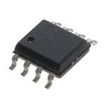
| 描述 | IC DIFF LINE DRVR/RCVR 8-SOICRS-485接口IC LP Diff Pairs |
| Duplex | Full Duplex |
| 产品分类 | |
| 品牌 | Texas Instruments |
| 产品手册 | |
| 产品图片 |
|
| rohs | 符合RoHS无铅 / 符合限制有害物质指令(RoHS)规范要求 |
| 产品系列 | 接口 IC,RS-485接口IC,Texas Instruments SN65LBC179D- |
| 数据手册 | |
| 产品型号 | SN65LBC179D |
| 产品目录页面 | |
| 产品种类 | RS-485接口IC |
| 供应商器件封装 | 8-SOIC |
| 关闭 | Yes |
| 其它名称 | 296-9727-5 |
| 功能 | Transceiver |
| 包装 | 管件 |
| 协议 | RS485 |
| 单位重量 | 72.600 mg |
| 双工 | 全 |
| 商标 | Texas Instruments |
| 安装类型 | 表面贴装 |
| 安装风格 | SMD/SMT |
| 封装 | Tube |
| 封装/外壳 | 8-SOIC(0.154",3.90mm 宽) |
| 封装/箱体 | SOIC-8 |
| 工作温度 | -40°C ~ 85°C |
| 工作温度范围 | - 40 C to + 85 C |
| 工作电源电压 | 5 V |
| 工厂包装数量 | 75 |
| 接收器滞后 | 50mV |
| 接收机数量 | 1 Receiver |
| 数据速率 | 30Mbps |
| 最大工作温度 | + 85 C |
| 最小工作温度 | - 40 C |
| 标准包装 | 75 |
| 激励器数量 | 1 Driver |
| 电压-电源 | 4.75 V ~ 5.25 V |
| 电源电流 | 5 mA |
| 类型 | 收发器 |
| 系列 | SN65LBC179 |
| 驱动器/接收器数 | 1/1 |


PDF Datasheet 数据手册内容提取
SN65LBC179A SN75LBC179A www.ti.com SLLS377D–MAY2000–REVISEDSEPTEMBER2011 LOW-POWER DIFFERENTIAL LINE DRIVER AND RECEIVER PAIRS CheckforSamples:SN65LBC179A,SN75LBC179A FEATURES 1 SN65LBC179AD (Marked as BL179A) • High-SpeedLow-PowerLinBiCMOS™Circuitry 2 SN65LBC179AP (Marked as 65LBC179A) DesignedforSignalingRates(1)ofupto30 SN75LBC179AD (Marked as LB179A) Mbps SN75LBC179AP (Marked as 75LBC179A) • Bus-PinESDProtectionExceeds12kVHBM (TOP VIEW) • VeryLowDisabledSupply-Current VCC 1 8 A Requirements...700μAMax R 2 7 B • Common-ModeVoltageRangeof–7Vto12V D 3 6 Z • LowSupplyCurrent...15mAMax GND 4 5 Y • CompatibleWithANSIStandardTIA/EAI-485-A andISO8482:1987(E) LOGICDIAGRAM(POSITIVELOGIC) • PositiveandNegativeOutputCurrentLimiting 8 • DriverThermalShutdownProtection 2 A R 7 (1)SignalingratebyTIA/EIA-485-Adefinitionrestricttransitiontimes B to30%ofthebitlength,andmuchhighersignalingratesmaybe achievedwithoutthisrequirementasdisplayedintheTYPICAL 5 CHARACTERISTICSofthisdevice. 3 Y D 6 Z DESCRIPTION The SN65LBC179A and SN75LBC179A differential driver and receiver pairs are monolithic integrated circuits designed for bidirectional data communication over long cables that take on the characteristics of transmission lines. They are balanced, or differential, voltage mode devices that are compatible with ANSI standard TIA/EIA-485-A and ISO 8482:1987(E). The A version offers improved switching performance over its predecessorswithoutsacrificingsignificantlymorepower. The SN65LBC179A and SN75LBC179A combine a differential line driver and differential input line receiver and operate from a single 5-V supply. The driver differential outputs and the receiver differential inputs are connected to separate terminals for full-duplex operation and are designed to present minimum loading to the bus when powered off (V = 0). These parts feature a wide positive and negative common-mode voltage range making CC them suitable for point-to-point or multipoint data bus applications. The devices also provide positive- and negative-currentlimitingandthermalshutdownforprotectionfromlinefaultconditions. The SN65LBC179A is characterized over the industrial temperature range of –40°C to 85°C. The SN75LBC179A ischaracterizedforoperationoverthecommercialtemperaturerangeof0°Cto70°C. FUNCTIONTABLE(1) DRIVER RECEIVER DIFFERENTIALINPUTS OUTPUT INPUT OUTPUTS A–B R D Y Z V ≥0.2V H ID H H L -0.2V<V <0.2V ? ID L L H V ≤-0.2V L ID OPEN H L Opencircuit H (1) H=highlevel,L=lowlevel,?=indeterminate 1 Pleasebeawarethatanimportantnoticeconcerningavailability,standardwarranty,anduseincriticalapplicationsofTexas Instrumentssemiconductorproductsanddisclaimerstheretoappearsattheendofthisdatasheet. LinBiCMOSisatrademarkofTexasInstruments. 2 PRODUCTIONDATAinformationiscurrentasofpublicationdate. Copyright©2000–2011,TexasInstrumentsIncorporated Products conform to specifications per the terms of the Texas Instruments standard warranty. Production processing does not necessarilyincludetestingofallparameters.
SN65LBC179A SN75LBC179A SLLS377D–MAY2000–REVISEDSEPTEMBER2011 www.ti.com Thesedeviceshavelimitedbuilt-inESDprotection.Theleadsshouldbeshortedtogetherorthedeviceplacedinconductivefoam duringstorageorhandlingtopreventelectrostaticdamagetotheMOSgates. AVAILABLEOPTIONS PACKAGE TA SMALLOUTLINE PLASTIC (D) DUAL-IN-LINE 0°Cto70°C SN75LBC179AD SN75LBC179AP –40°Cto85°C SN65LBC179AD SN65LBC179AP SCHEMATICS OF INPUTS AND OUTPUTS D Inputs VCC 100 kΩ 1 kΩ Input 8 V AInput B Input VCC VCC 16 V 100 kΩ 16 V 4 kΩ 4 kΩ 18 kΩ 18 kΩ Input Input 100 kΩ 16 V 16 V 4 kΩ 4 kΩ YAND Z Outputs VCC R Output VCC 16 V Receiver 40Ω Output Output 8 V 16 V Receiver 2 SubmitDocumentationFeedback Copyright©2000–2011,TexasInstrumentsIncorporated ProductFolderLink(s):SN65LBC179ASN75LBC179A
SN65LBC179A SN75LBC179A www.ti.com SLLS377D–MAY2000–REVISEDSEPTEMBER2011 ABSOLUTE MAXIMUM RATINGS(1) overoperatingfree-airtemperaturerange(unlessotherwisenoted) UNIT V Supplyvoltagerange(2) –0.3Vto6V CC A,B,Y,orZ(2) –10Vto15V Voltagerange DorR(2) –0.3VtoV +0.5V CC I Receiveroutputcurrent ±20mA O BusterminalsandGND,Class3,A(3) 12kV BusterminalsandGND,Class3,B(3) 400V Electrostaticdischarge Allterminals,Class3,A 3kV Allterminals,Class3,B 400V Continuoustotalpowerdissipation(4) Internallylimited Totalpowerdissipation SeeDissipationRatingTable (1) Stressesbeyondthoselistedunderabsolutemaximumratingsmaycausepermanentdamagetothedevice.Thesearestressratings only,andfunctionaloperationofthedeviceattheseoranyotherconditionsbeyondthoseindicatedunderrecommendedoperating conditionsisnotimplied.Exposuretoabsolute-maximum-ratedconditionsforextendedperiodsmayaffectdevicereliability. (2) Allvoltagevalues,exceptdifferentialI/Obusvoltages,arewithrespecttoGND. (3) TestedinaccordancewithMIL-STD-883C,Method3015.7 (4) Themaximumoperatingjunctiontemperatureisinternallylimited.Usesthedissipationratingtabletooperatebelowthistemperature. DISSIPATION RATINGS PACKAGE T ≤25°C DERATINGFACTOR(1) T =70°C T =85°C A A A POWERRATING ABOVET =25°C POWERRATING POWERRATING A D 725mW 5.8mW/°C 464mW 377mW P 1100mW 8.08mW/°C 640mW 520mW (1) Thisistheinverseofthejunction-to-ambientthermalresistancewhenboard-mountedandwithnoairflow. RECOMMENDED OPERATING CONDITIONS MIN NOM MAX UNIT V Supplyvoltage 4.75 5 5.25 V CC V High-levelinputvoltage D 2 V V IH CC V Low-levelinputvoltage D 0 0.8 V IL V Differentialinputvoltage(1) –12(2) 12 V ID V O V Voltageatanybusterminal(separatelyorcommon-mode) A,B,Y,orZ –7 12 V I V IC YorZ –60 I High-leveloutputcurrent mA OH R –8 YorZ 60 I Low-leveloutputcurrent mA OL R 8 SN65LBC179A –40 85 T Operatingfree-airtemperature °C A SN75LBC179A 0 70 (1) Differentialinput/outputbusvoltageismeasuredatthenoninvertingterminalwithrespecttotheinvertingterminal. (2) Thealgebraicconvention,inwhichtheleastpositive(mostnegative)limitisdesignatedasminimum,isusedinthisdatasheet. Copyright©2000–2011,TexasInstrumentsIncorporated SubmitDocumentationFeedback 3 ProductFolderLink(s):SN65LBC179ASN75LBC179A
SN65LBC179A SN75LBC179A SLLS377D–MAY2000–REVISEDSEPTEMBER2011 www.ti.com DRIVER ELECTRICAL CHARACTERISTICS overrecommendedoperatingconditions(unlessotherwisenoted) PARAMETER TESTCONDITIONS MIN TYP(1) MAX UNIT V Inputclampvoltage I =–18mA –1.5 –0.8 V IK I SN65LBC179A 1 1.5 3 R =54Ω,SeeFigure1 V L SN75LBC179A 1.1 1.5 3 |V | Differentialoutputvoltage OD R =60Ω,–7<V <12, SN65LBC179A 1 1.5 3 L (tot) V SeeFigure2 SN75LBC179A 1.1 1.5 3 Changeinmagnitudeofdifferentialoutput Δ|VOD| voltage (2) SeeFigure1andFigure2 –0.2 0.2 V Steady-statecommon-modeoutput V 1.8 2.4 2.8 V OC(SS) voltage SeeFigure1 Changeinsteady-statecommon-mode ΔVOC(SS) outputvoltage(2) –0.1 0.1 V I Outputcurrentwithpoweroff V =0, V =–7Vto12V –10 ±1 10 μA O CC O I High-levelinputcurrent V =2.V –100 μA IH I I Low-levelinputcurrent V =0.8V –100 μA IL I I Short-circuitoutputcurrent –7V≤V ≤12V –250 ±70 250 mA OS O I Supplycurrent Noload, V =0orV 8.5 15 mA CC I CC (1) AlltypicalvaluesareatV =5V,T =25°C. CC A (2) Δ|V |andΔ|V |arethechangesinthesteady-statemagnitudeofV andV ,respectively,thatoccurwhentheinputis OD OC OD OC changedfromahighleveltoalowlevel. DRIVER SWITCHING CHARACTERISTICS overrecommendedoperatingconditions(unlessotherwisenoted) PARAMETER TESTCONDITIONS MIN TYP MAX UNIT t Propagationdelaytime,low-to-high-leveloutput 2 6 12 ns PLH t Propagationdelaytime,high-to-low-leveloutput 2 6 12 ns PHL t Pulseskew(|t –t |) R =54Ω,C =50pF,SeeFigure3 0.3 1 ns sk(p) PHL PLH L L t Differentialoutputsignalrisetime 4 7.5 11 ns r t Differentialoutputsignalfalltime 4 7.5 11 ns f 4 SubmitDocumentationFeedback Copyright©2000–2011,TexasInstrumentsIncorporated ProductFolderLink(s):SN65LBC179ASN75LBC179A
SN65LBC179A SN75LBC179A www.ti.com SLLS377D–MAY2000–REVISEDSEPTEMBER2011 RECEIVER SECTION RECEIVER ELECTRICAL CHARACTERISTICS overrecommendedoperatingconditions(unlessotherwisenoted) PARAMETER TESTCONDITIONS MIN TYP MAX UNIT V Positive-goinginputthresholdvoltage I =–8mA 0.2 IT+ O V V Negative-goinginputthresholdvoltage –0.2 IT– I =8mA O V Hysteresisvoltage(V –V ) 50 mV hys IT+ IT– V High-leveloutputvoltage V =200mV,I =–8mA,SeeFigure1 4 4.9 V OH ID OH V Low-leveloutputvoltage V =–200mV,I =8mA,SeeFigure1 0.1 0.8 V OL ID OL V =12V,V =5V 0.4 1 IH CC V =12V,V =0 0.5 1 IH CC I Businputcurrent Otherinputat0V mA I V =–7V,V =5V –0.8 –0.4 IH CC V =–7V,V =0 –0.8 –0.3 IH CC RECEIVER SWITCHING CHARACTERISTICS overrecommendedoperatingconditions(unlessotherwisenoted) PARAMETER TESTCONDITIONS MIN TYP MAX UNIT t Propagationdelaytime,low-to-high-leveloutput 7 13 20 ns PLH t Propagationdelaytime,high-to-low-leveloutput 7 13 20 ns PHL V =–1.5Vto1.5V,SeeFigure4 ID t Pulseskew(|t –t |) 0.5 1.5 ns sk(p) PLH PHL t Risetime,output 2.1 3.3 ns r t Falltime,output SeeFigure4 2.1 3.3 ns f PARAMETER MEASURMENT INFORMATION Y 27 W D 0 V or 3 V VOD 27 W VOC Z Figure1. DriverV andV OD OC V(test ) R1 375 W Y 0 V or 3 V D RL = 60 W VOD Z R2 −7 V < V(test) < 12 V 375 W V(test ) Figure2. DriverV WithCommon-ModeLoading OD Copyright©2000–2011,TexasInstrumentsIncorporated SubmitDocumentationFeedback 5 ProductFolderLink(s):SN65LBC179ASN75LBC179A
SN65LBC179A SN75LBC179A SLLS377D–MAY2000–REVISEDSEPTEMBER2011 www.ti.com PARAMETER MEASURMENT INFORMATION (continued) 3 V Input 1.5 V 1.5 V CL = 50 pF 0 V (see Note B) Generator 50 W RL = 54 W Output tPLH tPHL (see Note A) ≈ 1.5 V 90% Output 50% 50% 10% ≈ − 1.5 V tr tf TEST CIRCUIT VOLTAGE WAVEFORMS A. Theinputpulseissuppliedbyageneratorhavingthefollowingcharacteristics:PRR≤1MHz,50%dutycycle,t ≤6 r ns,t ≤6ns,Z =50Ω. f O B. C includesprobeandjigcapacitance. L Figure3. DriverTestCircuitsandVoltageWaveforms 3 V Input 1.5 V 1.5 V A 0 V Generator (see Note A) 50 W B Output tPLH tPHL 1.5 V VOH CL = 15 pF 90% 90% (see Note B) Output 1.3 V 1.3 V 10% 10% VOL tr tf TEST CIRCUIT VOLTAGE WAVEFORMS A. Theinputpulseissuppliedbyageneratorhavingthefollowingcharacteristics:PRR≤1MHz,50%dutycycle,t ≤6 r ns,t ≤6ns,Z =50Ω. f O B. CLincludesprobeandjigcapacitance. Figure4. ReceiverTestCircuitandVoltageWaveforms 6 SubmitDocumentationFeedback Copyright©2000–2011,TexasInstrumentsIncorporated ProductFolderLink(s):SN65LBC179ASN75LBC179A
SN65LBC179A SN75LBC179A www.ti.com SLLS377D–MAY2000–REVISEDSEPTEMBER2011 TYPICAL CHARACTERISTICS Receiver Output Driver Input 120 W 120 W Driver Input Receiver Output Figure5. TypicalWaveformofNon-Return-To-Zero(NRZ),PseudorandomBinarySequence(PRBS) Dataat100MbpsThrough15m,ofCAT5UnshieldedTwistedPair(UTP)Cable TIA/EIA-485-A defines a maximum signaling rate as that in which the transition time of the voltage transition of a logic-state change remains less than or equal to 30% of the bit length. Transition times of greater length perform quitewelleventhoughtheydonotmeetthestandardbydefinition. AVERAGESUPPLYCURRENT LOGICINPUTCURRENT vs vs FREQUENCY INPUTVOLTAGE 45 −30 40 Driver −25 A m 35 − A y Current 2350 mCurrent − −20 ppl ut −15 Su 20 np erage 15 Logic I −10 Av Receiver − − 10 II C C −5 I 5 0 0 0.05 0.5 1 2 5 10 20 30 0 1 2 3 4 5 f − Frequency − MHz VI − Input Voltage − V Figure6. Figure7. Copyright©2000–2011,TexasInstrumentsIncorporated SubmitDocumentationFeedback 7 ProductFolderLink(s):SN65LBC179ASN75LBC179A
SN65LBC179A SN75LBC179A SLLS377D–MAY2000–REVISEDSEPTEMBER2011 www.ti.com TYPICAL CHARACTERISTICS (continued) INPUTCURRENT LOW-LEVELOUTPUTVOLTAGE vs vs INPUTVOLTAGE LOW-LEVELOUTPUTCURRENT 800 2.00 600 V 1.75 − e A g m− 400 Volta 1.50 VCC = 5 nt ut 1.25 e p Curr 200 Out − Input 0 w-Level 01..7050 o II−200 − L L 0.50 Bus Input Current VO −400 0.25 −600 0.00 −8 −6 −4 −2 0 2 4 6 8 10 12 0 10 20 30 40 50 60 70 80 VI − Input Voltage − V IOL − Low-Level Output Current − mA Figure8. Figure9. DRIVERHIGH-LEVELOUTPUTVOLTAGE DRIVERDIFFERENTIALOUTPUTVOLTAGE vs vs HIGH-LEVELOUTPUTCURRENT AVERAGECASETEMPERATURE 5 2 − V 4.5 − V e e g g olta 4 VCC = 5.25 V olta 1.5 V V ut 3.5 ut p p ut 3 ut O O el al ev 2.5 VCC = 5 V nti 1 L e High- 2 VCC = 4.75 V Differ er 1.5 er v v Dri Dri 0.5 − 1 − H D O 0.5 O V V 0 0 0 −10 −20 −30 −40 −50 −60 −70 −80 −40 0 25 70 85 IO H − High-Level Output Current − (mA) Average Case Temperature − ° C Figure10. Figure11. 8 SubmitDocumentationFeedback Copyright©2000–2011,TexasInstrumentsIncorporated ProductFolderLink(s):SN65LBC179ASN75LBC179A
SN65LBC179A SN75LBC179A www.ti.com SLLS377D–MAY2000–REVISEDSEPTEMBER2011 TYPICAL CHARACTERISTICS (continued) RECEIVERPROPAGATIONTIME DRIVERPROPAGATIONDELAYTIME vs vs CASETEMPERATURE CASETEMPERATURE 13.8 7.4 13.7 s 7.2 n − − ns 13.6 me 7 e Ti m y n Ti 13.5 Dela 6.8 atio 13.4 on 6.6 ag ati p g Pro 13.3 opa 6.4 Receiver 1133..12 Driver Pr 6.26 − − PHL 13 PHL 5.8 TT T 12.9 5.6 −40 0 25 70 80 −40 0 25 70 85 Case Temperature ° C Case Temperature − ° C Figure12. Figure13. DRIVEROUTPUTCURRENT vs SUPPLYVOLTAGE 90 65 A 40 m − 15 ent −10 IOH Curr −35 ut p −60 ut O −85 er Driv −110 − −135 IOL I O −160 −185 −210 0 3 4 5 6 VCC − Supply Voltage − V Figure14. Copyright©2000–2011,TexasInstrumentsIncorporated SubmitDocumentationFeedback 9 ProductFolderLink(s):SN65LBC179ASN75LBC179A
SN65LBC179A SN75LBC179A SLLS377D–MAY2000–REVISEDSEPTEMBER2011 www.ti.com REVISION HISTORY ChangesfromRevisionC(June2001)toRevisionD Page • ChangedtheDOutputandROutputschematins ................................................................................................................ 2 • AddedReceiveroutputcurrenttotheAbsMaxTable.......................................................................................................... 3 • ChangedESD-Allterminals,Class3,AFrom:4kVTo:3kV ............................................................................................ 3 10 SubmitDocumentationFeedback Copyright©2000–2011,TexasInstrumentsIncorporated ProductFolderLink(s):SN65LBC179ASN75LBC179A
PACKAGE OPTION ADDENDUM www.ti.com 6-Feb-2020 PACKAGING INFORMATION Orderable Device Status Package Type Package Pins Package Eco Plan Lead/Ball Finish MSL Peak Temp Op Temp (°C) Device Marking Samples (1) Drawing Qty (2) (6) (3) (4/5) SN65LBC179AD ACTIVE SOIC D 8 75 Green (RoHS NIPDAU Level-1-260C-UNLIM -40 to 85 BL179A & no Sb/Br) SN65LBC179ADG4 ACTIVE SOIC D 8 75 Green (RoHS NIPDAU Level-1-260C-UNLIM -40 to 85 BL179A & no Sb/Br) SN65LBC179ADR ACTIVE SOIC D 8 2500 Green (RoHS NIPDAU Level-1-260C-UNLIM -40 to 85 BL179A & no Sb/Br) SN65LBC179ADRG4 ACTIVE SOIC D 8 2500 Green (RoHS NIPDAU Level-1-260C-UNLIM -40 to 85 BL179A & no Sb/Br) SN65LBC179AP ACTIVE PDIP P 8 50 Green (RoHS NIPDAU N / A for Pkg Type -40 to 85 65LBC179A & no Sb/Br) SN75LBC179AD ACTIVE SOIC D 8 75 Green (RoHS NIPDAU Level-1-260C-UNLIM 0 to 70 LB179A & no Sb/Br) SN75LBC179ADG4 ACTIVE SOIC D 8 75 Green (RoHS NIPDAU Level-1-260C-UNLIM 0 to 70 LB179A & no Sb/Br) SN75LBC179ADR ACTIVE SOIC D 8 2500 Green (RoHS NIPDAU Level-1-260C-UNLIM 0 to 70 LB179A & no Sb/Br) SN75LBC179ADRG4 ACTIVE SOIC D 8 2500 Green (RoHS NIPDAU Level-1-260C-UNLIM 0 to 70 LB179A & no Sb/Br) SN75LBC179AP ACTIVE PDIP P 8 50 Green (RoHS NIPDAU N / A for Pkg Type 0 to 70 75LBC179A & no Sb/Br) (1) The marketing status values are defined as follows: ACTIVE: Product device recommended for new designs. LIFEBUY: TI has announced that the device will be discontinued, and a lifetime-buy period is in effect. NRND: Not recommended for new designs. Device is in production to support existing customers, but TI does not recommend using this part in a new design. PREVIEW: Device has been announced but is not in production. Samples may or may not be available. OBSOLETE: TI has discontinued the production of the device. (2) RoHS: TI defines "RoHS" to mean semiconductor products that are compliant with the current EU RoHS requirements for all 10 RoHS substances, including the requirement that RoHS substance do not exceed 0.1% by weight in homogeneous materials. Where designed to be soldered at high temperatures, "RoHS" products are suitable for use in specified lead-free processes. TI may reference these types of products as "Pb-Free". RoHS Exempt: TI defines "RoHS Exempt" to mean products that contain lead but are compliant with EU RoHS pursuant to a specific EU RoHS exemption. Green: TI defines "Green" to mean the content of Chlorine (Cl) and Bromine (Br) based flame retardants meet JS709B low halogen requirements of <=1000ppm threshold. Antimony trioxide based flame retardants must also meet the <=1000ppm threshold requirement. (3) MSL, Peak Temp. - The Moisture Sensitivity Level rating according to the JEDEC industry standard classifications, and peak solder temperature. Addendum-Page 1
PACKAGE OPTION ADDENDUM www.ti.com 6-Feb-2020 (4) There may be additional marking, which relates to the logo, the lot trace code information, or the environmental category on the device. (5) Multiple Device Markings will be inside parentheses. Only one Device Marking contained in parentheses and separated by a "~" will appear on a device. If a line is indented then it is a continuation of the previous line and the two combined represent the entire Device Marking for that device. (6) Lead/Ball Finish - Orderable Devices may have multiple material finish options. Finish options are separated by a vertical ruled line. Lead/Ball Finish values may wrap to two lines if the finish value exceeds the maximum column width. Important Information and Disclaimer:The information provided on this page represents TI's knowledge and belief as of the date that it is provided. TI bases its knowledge and belief on information provided by third parties, and makes no representation or warranty as to the accuracy of such information. Efforts are underway to better integrate information from third parties. TI has taken and continues to take reasonable steps to provide representative and accurate information but may not have conducted destructive testing or chemical analysis on incoming materials and chemicals. TI and TI suppliers consider certain information to be proprietary, and thus CAS numbers and other limited information may not be available for release. In no event shall TI's liability arising out of such information exceed the total purchase price of the TI part(s) at issue in this document sold by TI to Customer on an annual basis. Addendum-Page 2
PACKAGE MATERIALS INFORMATION www.ti.com 5-May-2010 TAPE AND REEL INFORMATION *Alldimensionsarenominal Device Package Package Pins SPQ Reel Reel A0 B0 K0 P1 W Pin1 Type Drawing Diameter Width (mm) (mm) (mm) (mm) (mm) Quadrant (mm) W1(mm) SN65LBC179ADR SOIC D 8 2500 330.0 12.4 6.4 5.2 2.1 8.0 12.0 Q1 SN75LBC179ADR SOIC D 8 2500 330.0 12.4 6.4 5.2 2.1 8.0 12.0 Q1 PackMaterials-Page1
PACKAGE MATERIALS INFORMATION www.ti.com 5-May-2010 *Alldimensionsarenominal Device PackageType PackageDrawing Pins SPQ Length(mm) Width(mm) Height(mm) SN65LBC179ADR SOIC D 8 2500 340.5 338.1 20.6 SN75LBC179ADR SOIC D 8 2500 340.5 338.1 20.6 PackMaterials-Page2
PACKAGE OUTLINE D0008A SOIC - 1.75 mm max height SCALE 2.800 SMALL OUTLINE INTEGRATED CIRCUIT C SEATING PLANE .228-.244 TYP [5.80-6.19] .004 [0.1] C A PIN 1 ID AREA 6X .050 [1.27] 8 1 2X .189-.197 [4.81-5.00] .150 NOTE 3 [3.81] 4X (0 -15 ) 4 5 8X .012-.020 B .150-.157 [0.31-0.51] .069 MAX [3.81-3.98] .010 [0.25] C A B [1.75] NOTE 4 .005-.010 TYP [0.13-0.25] 4X (0 -15 ) SEE DETAIL A .010 [0.25] .004-.010 0 - 8 [0.11-0.25] .016-.050 [0.41-1.27] DETAIL A (.041) TYPICAL [1.04] 4214825/C 02/2019 NOTES: 1. Linear dimensions are in inches [millimeters]. Dimensions in parenthesis are for reference only. Controlling dimensions are in inches. Dimensioning and tolerancing per ASME Y14.5M. 2. This drawing is subject to change without notice. 3. This dimension does not include mold flash, protrusions, or gate burrs. Mold flash, protrusions, or gate burrs shall not exceed .006 [0.15] per side. 4. This dimension does not include interlead flash. 5. Reference JEDEC registration MS-012, variation AA. www.ti.com
EXAMPLE BOARD LAYOUT D0008A SOIC - 1.75 mm max height SMALL OUTLINE INTEGRATED CIRCUIT 8X (.061 ) [1.55] SYMM SEE DETAILS 1 8 8X (.024) [0.6] SYMM (R.002 ) TYP [0.05] 5 4 6X (.050 ) [1.27] (.213) [5.4] LAND PATTERN EXAMPLE EXPOSED METAL SHOWN SCALE:8X SOLDER MASK SOLDER MASK METAL OPENING OPENING METAL UNDER SOLDER MASK EXPOSED METAL EXPOSED METAL .0028 MAX .0028 MIN [0.07] [0.07] ALL AROUND ALL AROUND NON SOLDER MASK SOLDER MASK DEFINED DEFINED SOLDER MASK DETAILS 4214825/C 02/2019 NOTES: (continued) 6. Publication IPC-7351 may have alternate designs. 7. Solder mask tolerances between and around signal pads can vary based on board fabrication site. www.ti.com
EXAMPLE STENCIL DESIGN D0008A SOIC - 1.75 mm max height SMALL OUTLINE INTEGRATED CIRCUIT 8X (.061 ) [1.55] SYMM 1 8 8X (.024) [0.6] SYMM (R.002 ) TYP [0.05] 5 4 6X (.050 ) [1.27] (.213) [5.4] SOLDER PASTE EXAMPLE BASED ON .005 INCH [0.125 MM] THICK STENCIL SCALE:8X 4214825/C 02/2019 NOTES: (continued) 8. Laser cutting apertures with trapezoidal walls and rounded corners may offer better paste release. IPC-7525 may have alternate design recommendations. 9. Board assembly site may have different recommendations for stencil design. www.ti.com
None
IMPORTANTNOTICEANDDISCLAIMER TI PROVIDES TECHNICAL AND RELIABILITY DATA (INCLUDING DATASHEETS), DESIGN RESOURCES (INCLUDING REFERENCE DESIGNS), APPLICATION OR OTHER DESIGN ADVICE, WEB TOOLS, SAFETY INFORMATION, AND OTHER RESOURCES “AS IS” AND WITH ALL FAULTS, AND DISCLAIMS ALL WARRANTIES, EXPRESS AND IMPLIED, INCLUDING WITHOUT LIMITATION ANY IMPLIED WARRANTIES OF MERCHANTABILITY, FITNESS FOR A PARTICULAR PURPOSE OR NON-INFRINGEMENT OF THIRD PARTY INTELLECTUAL PROPERTY RIGHTS. These resources are intended for skilled developers designing with TI products. You are solely responsible for (1) selecting the appropriate TI products for your application, (2) designing, validating and testing your application, and (3) ensuring your application meets applicable standards, and any other safety, security, or other requirements. These resources are subject to change without notice. TI grants you permission to use these resources only for development of an application that uses the TI products described in the resource. Other reproduction and display of these resources is prohibited. No license is granted to any other TI intellectual property right or to any third party intellectual property right. TI disclaims responsibility for, and you will fully indemnify TI and its representatives against, any claims, damages, costs, losses, and liabilities arising out of your use of these resources. TI’s products are provided subject to TI’s Terms of Sale (www.ti.com/legal/termsofsale.html) or other applicable terms available either on ti.com or provided in conjunction with such TI products. TI’s provision of these resources does not expand or otherwise alter TI’s applicable warranties or warranty disclaimers for TI products. Mailing Address: Texas Instruments, Post Office Box 655303, Dallas, Texas 75265 Copyright © 2020, Texas Instruments Incorporated