ICGOO在线商城 > 集成电路(IC) > 接口 - 驱动器,接收器,收发器 > SN65HVD72DGKR

 Datasheet下载
- 型号: SN65HVD72DGKR
- 制造商: Texas Instruments
- 库位|库存: xxxx|xxxx
- 要求:
| 数量阶梯 | 香港交货 | 国内含税 |
| +xxxx | $xxxx | ¥xxxx |
查看当月历史价格
查看今年历史价格
SN65HVD72DGKR产品简介:
ICGOO电子元器件商城为您提供SN65HVD72DGKR由Texas Instruments设计生产,在icgoo商城现货销售,并且可以通过原厂、代理商等渠道进行代购。 SN65HVD72DGKR价格参考¥17.55-¥21.94。Texas InstrumentsSN65HVD72DGKR封装/规格:接口 - 驱动器,接收器,收发器, 1/1 Transceiver Half RS422, RS485 8-VSSOP。您可以下载SN65HVD72DGKR参考资料、Datasheet数据手册功能说明书,资料中有SN65HVD72DGKR 详细功能的应用电路图电压和使用方法及教程。
SN65HVD72DGKR是德州仪器(Texas Instruments)推出的一款高性能CAN收发器,属于接口类驱动器/收发器产品。该器件主要应用于控制器局域网(CAN)通信系统中,作为微控制器与物理总线之间的接口,支持高速、可靠的双向数据传输。

典型应用场景包括工业自动化控制系统,如PLC(可编程逻辑控制器)、工业传感器和现场总线通信模块,其高抗干扰能力和稳定性能适应复杂的工业电磁环境。在电动汽车和新能源领域,该芯片用于电池管理系统(BMS)、电机控制器和车载充电模块之间的CAN通信,保障实时、安全的数据交互。此外,还广泛应用于楼宇自动化、智能电网设备以及农业和工程机械的电控单元(ECU)中。

SN65HVD72DGKR采用8引脚VSSOP封装,具备低功耗待机模式、热关断保护和故障隔离功能,支持1 Mbps以上的数据速率,兼容ISO 11898标准,适用于-40°C至+125°C的宽温工作范围,适合严苛环境下的可靠运行。其小尺寸和高集成度也便于在空间受限的嵌入式系统中使用。
| 参数 | 数值 |
| 产品目录 | 集成电路 (IC)半导体 |
| 描述 | IC TXRX RS485 3.3V 8VSSOPRS-485接口IC 3.3V-Supply RS-485 IEC ESD Protection |
| Duplex | Half Duplex |
| 产品分类 | |
| 品牌 | Texas Instruments |
| 产品手册 | |
| 产品图片 |
|
| rohs | 符合RoHS无铅 / 符合限制有害物质指令(RoHS)规范要求 |
| 产品系列 | 接口 IC,RS-485接口IC,Texas Instruments SN65HVD72DGKR- |
| 数据手册 | |
| 产品型号 | SN65HVD72DGKR |
| PCN设计/规格 | |
| 产品种类 | RS-485接口IC |
| 传播延迟时间ns | 0.7 us |
| 供应商器件封装 | * |
| 关闭 | No |
| 其它名称 | 296-35069-2 |
| 功能 | Transceivers |
| 包装 | 带卷 (TR) |
| 协议 | RS485 |
| 双工 | 半 |
| 商标 | Texas Instruments |
| 安装类型 | * |
| 安装风格 | SMD/SMT |
| 封装 | Reel |
| 封装/外壳 | 8-TSSOP,8-MSOP(0.118",3.00mm 宽) |
| 封装/箱体 | VSSOP-8 |
| 工作温度 | -40°C ~ 125°C |
| 工作温度范围 | - 40 C to + 125 C |
| 工作电源电压 | 3.3 V |
| 工厂包装数量 | 2500 |
| 接收器滞后 | 80mV |
| 接收机数量 | 1 |
| 数据速率 | 250kbps |
| 最大工作温度 | + 125 C |
| 最小工作温度 | - 40 C |
| 标准包装 | 2,500 |
| 激励器数量 | 1 |
| 电压-电源 | 3 V ~ 3.6 V |
| 电源电流 | 750 uA |
| 类型 | 收发器 |
| 输入电压 | 3.3 V |
| 输出电压 | 2 V |
| 输出电流 | 60 mA, 8 mA |
| 驱动器/接收器数 | 1/1 |


- 商务部:美国ITC正式对集成电路等产品启动337调查
- 曝三星4nm工艺存在良率问题 高通将骁龙8 Gen1或转产台积电
- 太阳诱电将投资9.5亿元在常州建新厂生产MLCC 预计2023年完工
- 英特尔发布欧洲新工厂建设计划 深化IDM 2.0 战略
- 台积电先进制程称霸业界 有大客户加持明年业绩稳了
- 达到5530亿美元!SIA预计今年全球半导体销售额将创下新高
- 英特尔拟将自动驾驶子公司Mobileye上市 估值或超500亿美元
- 三星加码芯片和SET,合并消费电子和移动部门,撤换高东真等 CEO
- 三星电子宣布重大人事变动 还合并消费电子和移动部门
- 海关总署:前11个月进口集成电路产品价值2.52万亿元 增长14.8%


PDF Datasheet 数据手册内容提取
Product Order Technical Tools & Support & Folder Now Documents Software Community SN65HVD72,SN65HVD75,SN65HVD78 SLLSE11H–MARCH2012–REVISEDMARCH2019 SN65HVD7x 3.3-V Supply RS-485 With IEC ESD protection 1 Features 2 Applications • Small-sizeVSSOPPackagesSaveBoardSpace, • FactoryAutomation 1 orSOICforDrop-inCompatibility • TelecommunicationsInfrastructure • BusI/OProtection • MotionControl – >±15kVHBMProtection 3 Description – >±12kVIEC61000-4-2ContactDischarge These devices have robust 3.3-V drivers and – >±4kVIEC61000-4-4FastTransientBurst receivers in a small package for demanding industrial • ExtendedIndustrialTemperatureRange applications. The bus pins are robust to ESD events –40°Cto125°C with high levels of protection to Human-Body Model • LargeReceiverHysteresis(80mV)forNoise andIECContactDischargespecifications. Rejection Each of these devices combines a differential driver • LowUnit-LoadingAllowsOver200Connected and a differential receiver which operate from a single Nodes 3.3-V power supply. The driver differential outputs and the receiver differential inputs are connected • LowPowerConsumption internally to form a bus port suitable for half-duplex – LowStandbySupplyCurrent: < 2µA (two-wire bus) communication. These devices feature – I < 1mAQuiescentDuringOperation a wide common-mode voltage range making the CC • 5-VTolerantLogicInputsCompatibleWith devices suitable for multi-point applications over long cable runs. These devices are characterized from 3.3-Vor5-VControllers –40°Cto125°C. • SignalingRateOptionsOptimizedfor: 250kbps,20Mbps,50Mbps DeviceInformation(1) • GlitchFreePower-UpandPower-DownBus PARTNUMBER PACKAGE BODYSIZE(NOM) InputsandOutputs SOIC(8) 4.91mm×3.90mm SN65HVD72, SN65HVD75, VSSOP(8) SN65HVD78 3.00mm×3.00mm VSON(8) (1) For all available packages, see the orderable addendum at theendofthedatasheet. TypicalApplicationDiagram R R R R A A RE RE B RT RT B DE DE D D D D A B A B R R D D R RE DE D R RE DE D Copyright © 2016, Texas Instruments Incorporated 1 An IMPORTANT NOTICE at the end of this data sheet addresses availability, warranty, changes, use in safety-critical applications, intellectualpropertymattersandotherimportantdisclaimers.UNLESSOTHERWISENOTED,thisdocumentcontainsPRODUCTION DATA.
SN65HVD72,SN65HVD75,SN65HVD78 SLLSE11H–MARCH2012–REVISEDMARCH2019 www.ti.com Table of Contents 1 Features.................................................................. 1 9.1 Overview.................................................................15 2 Applications........................................................... 1 9.2 FunctionalBlockDiagram.......................................15 3 Description............................................................. 1 9.3 FeatureDescription.................................................15 9.4 DeviceFunctionalModes........................................15 4 RevisionHistory..................................................... 2 10 ApplicationandImplementation........................ 17 5 DeviceComparisonTable..................................... 4 10.1 ApplicationInformation..........................................17 6 PinConfigurationandFunctions......................... 4 10.2 TypicalApplication................................................18 7 Specifications......................................................... 5 11 PowerSupplyRecommendations..................... 24 7.1 AbsoluteMaximumRatings......................................5 12 Layout................................................................... 25 7.2 ESDRatings..............................................................5 12.1 LayoutGuidelines.................................................25 7.3 RecommendedOperatingConditions.......................5 12.2 LayoutExample....................................................25 7.4 ThermalInformation..................................................6 13 DeviceandDocumentationSupport................. 26 7.5 ElectricalCharacteristics...........................................6 7.6 PowerDissipation.....................................................7 13.1 DeviceSupport......................................................26 7.7 SwitchingCharacteristics:250kbpsDevice 13.2 DocumentationSupport........................................26 (SN65HVD72)BitTime≥4µs...................................7 13.3 RelatedLinks........................................................26 7.8 SwitchingCharacteristics:20MbpsDevice 13.4 CommunityResources..........................................26 (SN65HVD75)BitTime≥50ns..................................8 13.5 Trademarks...........................................................26 7.9 SwitchingCharacteristics:50MbpsDevice 13.6 ElectrostaticDischargeCaution............................26 (SN65HVD78)BitTime≥20ns..................................8 13.7 Glossary................................................................26 7.10 TypicalCharacteristics............................................9 14 Mechanical,Packaging,andOrderable 8 ParameterMeasurementInformation................11 Information........................................................... 27 9 DetailedDescription............................................ 15 4 Revision History NOTE:Pagenumbersforpreviousrevisionsmaydifferfrompagenumbersinthecurrentversion. ChangesfromRevisionG(Januarly2019)toRevisionH Page • ChangedthePinConfigurationimages.................................................................................................................................. 4 • ChangedSupplyvoltage,V MAXvalueFrom=3.6VTo:5VintheAbsoluteMaximumRatingstable........................... 5 CC • Deleted"orRpin"forV intheAbsoluteMaximumRatings ............................................................................................... 5 CC • AddedreliabilitynotetoV intheRecommendedOperatingConditionstable.................................................................... 5 CC ChangesfromRevisionF(December2016)toRevisionG Page • ChangedFrom:Supplyvoltage,V MAXvalue=5.5VTo:Supplyvoltage,V orRpinMAXvalue=3.6Vinthe CC CC AbsoluteMaximumRatingstable........................................................................................................................................... 5 • ChangedFrom:InputvoltageatanylogicpinTo:VoltageatD,DE,orREintheAbsoluteMaximumRatingstable..........5 ChangesfromRevisionE(September2016)toRevisionF Page • ChangedpinAFrom:7To:6,andpinBFrom:6To:7inFigure26.................................................................................. 22 ChangesfromRevisionD(July2015)toRevisionE Page • AddednewFeature:GlitchFreePower-UpandPower-DownBusInputsandOutputs ....................................................... 1 2 SubmitDocumentationFeedback Copyright©2012–2019,TexasInstrumentsIncorporated ProductFolderLinks:SN65HVD72 SN65HVD75 SN65HVD78
SN65HVD72,SN65HVD75,SN65HVD78 www.ti.com SLLSE11H–MARCH2012–REVISEDMARCH2019 ChangesfromRevisionC(September2013)toRevisionD Page • AddedPinConfigurationandFunctionssection,ESDRatingstable,FeatureDescriptionsection,DeviceFunctional Modes,ApplicationandImplementationsection,PowerSupplyRecommendationssection,Layoutsection,Device andDocumentationSupportsection,andMechanical,Packaging,andOrderableInformationsection .............................. 1 ChangesfromRevisionB(June2012)toRevisionC Page • DeletedFeature:>±12kVIEC61000-4-2Air-GapDischarge................................................................................................ 1 • AddedFootnote2totheAbsoluteMaximumRatingstable................................................................................................... 5 • ChangedtheSwitchingCharacteristicsconditionsstatementFrom:250kbpsdevices(SN65HVD70,71,72)bittime >4µsTo:250kbpsdevice(SN65HVD72)bittime≥4µs.................................................................................................... 7 • ChangedtheSwitchingCharacteristicsconditionsstatementFrom:250kbpsdevices(SN65HVD73,74,75)bittime >50nsTo:250kbpsdevice(SN65HVD75)bittime≥50ns................................................................................................ 8 • ChangedtheSwitchingCharacteristicsconditionsstatementFrom:250kbpsdevices(SN65HVD76,77,78)bittime >20nsTo:250kbpsdevice(SN65HVD78)bittime≥20ns ............................................................................................... 8 • Addednote:R =54ΩtoFigure6,Figure7,andFigure8.................................................................................................. 9 L • AddedtheDGKpackagetotheSN65HVD72,75,78LogicDiagram................................................................................. 15 • ReplacedtheLOW-POWERSTANDBYMODEsection...................................................................................................... 19 • AddedtexttotheTransientProtectionsection..................................................................................................................... 20 ChangesfromRevisionA(May2012)toRevisionB Page • AddedtheSON-8packageandNodescolumntoDeviceComparisonTable,...................................................................... 4 • ChangedtheVoltagerangeatAorBInputsMINvalueFrom:–8VTo:–13VintheAbsoluteMaximumRatingstable....5 • Addedfootnoteforfree-airtemperaturetotheRecommendedOperatingConditionstable.................................................. 5 • ChangedtheBusinputcurrent(disableddriver)TYPvaluesforHVD78V =12VFrom:150To:240andV =–7V I I From:–120To:–180.............................................................................................................................................................. 7 • Changed,ThermalInformation............................................................................................................................................... 7 • Changed,ThermalCharacteristics......................................................................................................................................... 7 • AddedTYPvaluestotheSwitchingCharacteristicstable...................................................................................................... 8 • AddedTYPvaluestotheSwitchingCharacteristicstable...................................................................................................... 8 • ChangedtheSN65HVD72,75,78LogicDiagram............................................................................................................... 15 • Addedsection:LOW-POWERSTANDBYMODE................................................................................................................ 19 ChangesfromOriginal(March2012)toRevisionA Page • AddedVALUEstotheThermalCharacteristicstableintheDEVICEINFORMATIONsection. ........................................... 7 • ChangedtheSwitchingCharacteristicsconditionstatementFrom:15kbpsdevices(SN65HVD73,74,75)bittime> 65nsTo:20Mbpsdevices(SN65HVD73,74,75)bittime>50ns...................................................................................... 8 • ChangedtheSwitchingCharacteristicsconditionstatementFrom:50kbpsdevices(SN65HVD76,77,78)bittime> 20nsTo:50Mbpsdevices(SN65HVD76,77,78)bittime>20ns...................................................................................... 8 • AddedFigure4toTypicalCharacteristics............................................................................................................................. 9 • AddedFigure5toTypicalCharacteristics............................................................................................................................. 9 • AddedFigure6toTypicalCharacteristics............................................................................................................................. 9 • AddedFigure7toTypicalCharacteristics............................................................................................................................. 9 • AddedFigure8toTypicalCharacteristics............................................................................................................................. 9 • AddedFigure9toTypicalCharacteristics............................................................................................................................. 9 • AddedApplicationInformationsectiontodatasheet........................................................................................................... 17 Copyright©2012–2019,TexasInstrumentsIncorporated SubmitDocumentationFeedback 3 ProductFolderLinks:SN65HVD72 SN65HVD75 SN65HVD78
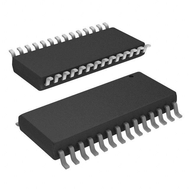
SN65HVD72,SN65HVD75,SN65HVD78 SLLSE11H–MARCH2012–REVISEDMARCH2019 www.ti.com 5 Device Comparison Table PARTNUMBER SIGNALINGRATE NODES DUPLEX ENABLES SN65HVD72 Upto250kbps 213 SN65HVD75 Upto20Mbps Half DE,RE SN65HVD78 Upto50Mbps 96 6 Pin Configuration and Functions DPackage 8-PinSOIC DGKPackage TopView 8-PinVSSOP TopView R 1 8 VCC R 1 8 VCC RE 2 7 B RE 2 7 B DE 3 6 A DE 3 6 A D 4 5 GND D 4 5 GND Not to scale Not to scale DRBPackage 8-PinVSON TopView R 1 8 VCC RE 2 7 B DE 3 6 A D 4 5 GND Not to scale PinFunctions PIN TYPE DESCRIPTION NAME NUMBER A 6 BusI/O Driveroutputorreceiverinput(complementarytoB) B 7 BusI/O Driveroutputorreceiverinput(complementarytoA) D 4 Digitalinput Driverdatainput DE 3 Digitalinput Active-highdriverenable GND 5 Referencepotential Localdeviceground R 1 Digitaloutput Receivedataoutput RE 2 Digitalinput Active-lowreceiverenable V 8 Supply 3-Vto3.6-Vsupply CC 4 SubmitDocumentationFeedback Copyright©2012–2019,TexasInstrumentsIncorporated ProductFolderLinks:SN65HVD72 SN65HVD75 SN65HVD78
SN65HVD72,SN65HVD75,SN65HVD78 www.ti.com SLLSE11H–MARCH2012–REVISEDMARCH2019 7 Specifications 7.1 Absolute Maximum Ratings overrecommendedoperatingrange(unlessotherwisespecified) (1) MIN MAX UNIT Supplyvoltage,V –0.5 5 CC VoltageatAorBinputs –13 16.5 V VoltageatD,DE,orRE –0.3 5.7 Voltageinput,transientpulse,AandB,through100Ω –100 100 Receiveroutputcurrent –24 24 mA Junctiontemperature,T 170 °C J Continuoustotalpowerdissipation SeePowerDissipation Storagetemperature,T –65 150 °C stg (1) StressesbeyondthoselistedunderAbsoluteMaximumRatingsmaycausepermanentdamagetothedevice.Thesearestressratings onlyandfunctionaloperationofthedeviceattheseoranyotherconditionsbeyondthoseindicatedunderRecommendedOperating Conditionsisnotimplied.Exposuretoabsolute-maximum-ratedconditionsforextendedperiodsmayaffectdevicereliability. 7.2 ESD Ratings VALUE UNIT Humanbodymodel(HBM),perANSI/ESDA/JEDECJS-001,allpins(1) ±8000 Chargeddevicemodel(CDM),perJEDECspecificationJESD22-C101or ANSI/ESDA/JEDECJS-002,allpins(2) ±1500 JEDECStandard22,TestMethodA115(MachineModel),allpins ±300 Electrostatic V(ESD) discharge IEC61000-4-2ESD(Air-GapDischarge),buspinsandGND (3) ±12000 V IEC61000-4-2ESD(ContactDischarge),buspinsandGND ±12000 IEC61000-4-4EFT(Fasttransientorburst)buspinsandGND ±4000 IEC60749-26ESD(HumanBodyModel),buspinsandGND ±15000 (1) JEDECdocumentJEP155statesthat500-VHBMallowssafemanufacturingwithastandardESDcontrolprocess. (2) JEDECdocumentJEP157statesthat250-VCDMallowssafemanufacturingwithastandardESDcontrolprocess. (3) Byinferencefromcontactdischargeresults,seeApplicationandImplementation. 7.3 Recommended Operating Conditions MIN NOM MAX UNIT V (1) Supplyvoltage 3 3.3 3.6 V CC V Inputvoltageatanybusterminal(separatelyorcommonmode)(2) –7 12 V I V High-levelinputvoltage(driver,driverenable,andreceiverenableinputs) 2 V V IH CC V Low-levelinputvoltage(driver,driverenable,andreceiverenableinputs) 0 0.8 V IL V Differentialinputvoltage –12 12 V ID I Outputcurrent,driver –60 60 mA O I Outputcurrent,receiver –8 8 mA O R Differentialloadresistance 54 60 Ω L C Differentialloadcapacitance 50 pF L SN65HVD72 250 kbps 1/t Signalingrate SN65HVD75 20 Mbps UI SN65HVD78 50 Mbps T (3) Operatingfree-airtemperature(SeeThermalInformation) –40 125 °C A T Junctiontemperature –40 150 °C J (1) Exposuretoconditionsbeyondtherecommendedoperationmaximumforextendedperiodsmayaffectdevicereliability. (2) Thealgebraicconvention,inwhichtheleastpositive(mostnegative)limitisdesignatedasminimum,isusedinthisdatasheet. (3) Operationisspecifiedforinternal(junction)temperaturesupto150°C.Self-heatingduetointernalpowerdissipationshouldbe consideredforeachapplication.Maximumjunctiontemperatureisinternallylimitedbythethermalshutdown(TSD)circuitwhichdisables thedriveroutputswhenthejunctiontemperaturereaches170°C. Copyright©2012–2019,TexasInstrumentsIncorporated SubmitDocumentationFeedback 5 ProductFolderLinks:SN65HVD72 SN65HVD75 SN65HVD78
SN65HVD72,SN65HVD75,SN65HVD78 SLLSE11H–MARCH2012–REVISEDMARCH2019 www.ti.com 7.4 Thermal Information SN65HVD72,SN65HVD75,SN65HVD78 THERMALMETRIC(1) D(SOIC) DGK(VSSOP) DRB(VSON) UNIT 8PINS R Junction-to-ambientthermalresistance 110.7 168.7 40 °C/W θJA R Junction-to-case(top)thermalresistance 54.7 62.2 49.6 °C/W θJC(top) R Junction-to-case(bottom)thermalresistance — — 3.9 °C/W θJC(bot) R Junction-to-boardthermalresistance 51.3 89.5 15.5 °C/W θJB ψ Junction-to-topcharacterizationparameter 9.2 7.4 0.6 °C/W JT ψ Junction-to-boardcharacterizationparameter 50.7 87.9 15.7 °C/W JB (1) Formoreinformationabouttraditionalandnewthermalmetrics,seetheSemiconductorandICPackageThermalMetricsapplication report. 7.5 Electrical Characteristics overrecommendedoperatingrange(unlessotherwisespecified) PARAMETER TESTCONDITIONS MIN TYP MAX UNIT R =60Ω,375Ωoneachoutputto See L 1.5 2 –7Vto12V Figure10 Driverdifferentialoutput |V | R =54Ω(RS-485) 1.5 2 V OD voltagemagnitude L R =100Ω(RS-422),T ≥0°C L J 2 2.5 V ≥3.2V CC Changeinmagnitudeof Δ|V | driverdifferentialoutput R =54Ω,C =50pF –50 0 50 mV OD L L voltage Steady-statecommon- See VOC(SS) modeoutputvoltage Centeroftwo27-Ωloadresistors Figure11 1 VCC/2 3 V Changeindifferential ΔV driveroutputcommon- Centeroftwo27-Ωloadresistors –50 0 50 mV OC modevoltage Peak-to-peakdriver V common-modeoutput Centeroftwo27-Ωloadresistors 200 mV OC(PP) voltage Differentialoutput C 15 pF OD capacitance Positive-goingreceiver V differentialinputvoltage See (1) –70 –20 mV IT+ threshold Negative-goingreceiver V differentialinputvoltage –200 –150 See (1) mV IT– threshold Receiverdifferential V inputvoltagethreshold 50 80 mV HYS hysteresis(V –V ) IT+ IT– Receiverhigh-level V I =–8mA 2.4 V –0.3 V OH outputvoltage OH CC Receiverlow-level V I =8mA 0.2 0.4 V OL outputvoltage OL Driverinput,driver I enable,andreceiver –2 2 µA I enableinputcurrent Receiveroutputhigh- I V =0VorV ,REatV –1 1 µA OZ impedancecurrent O CC CC Drivershort-circuit I –160 160 mA OS outputcurrent (1) Underanyspecificconditions,V isassuredtobeatleastV higherthanV . IT+ HYS IT– 6 SubmitDocumentationFeedback Copyright©2012–2019,TexasInstrumentsIncorporated ProductFolderLinks:SN65HVD72 SN65HVD75 SN65HVD78
SN65HVD72,SN65HVD75,SN65HVD78 www.ti.com SLLSE11H–MARCH2012–REVISEDMARCH2019 Electrical Characteristics (continued) overrecommendedoperatingrange(unlessotherwisespecified) PARAMETER TESTCONDITIONS MIN TYP MAX UNIT SN65HVD72 VI=12V 75 150 Businputcurrent VCC=3to3.6Vor SN65HVD75 VI=–7V –100 –40 I V =0V µA I (disableddriver) DCECat0V VI=12V 240 333 SN65HVD78 V =–7V –267 –180 I Driverandreceiver DE=V ,RE=GND CC 750 950 enabled Noload Driverenabled, DE=V ,RE=V CC CC 300 500 Supplycurrent receiverdisabled Noload I µA CC (quiescent) Driverdisabled, DE=GND,RE=GND 600 800 receiverenabled Noload Driverandreceiver DE=GND,D=open 0.1 2 disabled RE=V ,Noload CC Supplycurrent SeeTypicalCharacteristics (dynamic) Thermalshutdown T 170 °C TSD junctiontemperature 7.6 Power Dissipation PARAMETER TESTCONDITIONS VALUE UNIT SN65HVD72 120 R =300Ω L Unterminated C =50pF SN65HVD75 160 mW L PowerDissipation (driver) driverandreceiverenabled, SN65HVD78 200 VCC=3.6V,TJ=150°C SN65HVD72 155 50%dutycyclesquare-wavesignalat RL=100Ω PD signalingrate: RS-422load CL=50pF SN65HVD75 195 mW (driver) • SN65HVD72at250kbps SN65HVD78 230 • SN65HVD75at20Mbps SN65HVD72 190 • SN65HVD78at50Mbps RL=54Ω RS-485load C =50pF SN65HVD75 230 mW L (driver) SN65HVD78 260 7.7 Switching Characteristics: 250 kbps Device (SN65HVD72) Bit Time ≥ 4 µs overrecommendedoperatingconditions PARAMETER TESTCONDITIONS MIN TYP MAX UNIT DRIVER Driverdifferentialoutputriseor t,t 0.3 0.7 1.2 µs r f falltime R =54Ω L SeeFigure12 t ,t Driverpropagationdelay C =50pF 0.7 1 µs PHL PLH L t Driverpulseskew,|t –t | 0.2 µs SK(P) PHL PLH t ,t Driverdisabletime 0.1 0.4 µs PHZ PLZ SeeFigure13 Receiverenabled 0.5 1 t ,t Driverenabletime andFigure14 µs PZH PZL Receiverdisabled 3 9 RECEIVER t,t Receiveroutputriseorfalltime 12 30 ns r f t ,t Receiverpropagationdelaytime C =15pF SeeFigure15 75 100 ns PHL PLH L t Receiverpulseskew,|t –t | 3 15 ns SK(P) PHL PLH t ,t Receiverdisabletime 40 100 ns PLZ PHZ t ,t , Driverenabled SeeFigure16 20 50 ns PZL(1) PZH(1) Receiverenabletime tPZL(2),tPZH(2) Driverdisabled SeeFigure17 3 8 µs Copyright©2012–2019,TexasInstrumentsIncorporated SubmitDocumentationFeedback 7 ProductFolderLinks:SN65HVD72 SN65HVD75 SN65HVD78
SN65HVD72,SN65HVD75,SN65HVD78 SLLSE11H–MARCH2012–REVISEDMARCH2019 www.ti.com 7.8 Switching Characteristics: 20 Mbps Device (SN65HVD75) Bit Time ≥50 ns overrecommendedoperatingconditions PARAMETER TESTCONDITIONS MIN TYP MAX UNIT DRIVER Driverdifferentialoutputriseor t,t 2 7 14 ns r f falltime R =54Ω L SeeFigure12 t ,t Driverpropagationdelay C =50pF 7 11 17 ns PHL PLH L t Driverpulseskew,|t –t | 0 2 ns SK(P) PHL PLH t ,t Driverdisabletime 12 50 ns PHZ PLZ SeeFigure13 Receiverenabled 10 20 ns t ,t Driverenabletime andFigure14 PZH PZL Receiverdisabled 3 7 µs RECEIVER t,t Receiveroutputriseorfalltime 5 10 ns r f t ,t Receiverpropagationdelaytime C =15pF SeeFigure15 60 70 ns PHL PLH L t Receiverpulseskew,|t –t | 0 6 ns SK(P) PHL PLH t ,t Receiverdisabletime 15 30 ns PLZ PHZ t ,t , Driverenabled SeeFigure16 10 50 ns pZL(1) PZH(1) Receiverenabletime tPZL(2),tPZH(2) Driverdisabled SeeFigure17 3 8 µs 7.9 Switching Characteristics: 50 Mbps Device (SN65HVD78) Bit Time ≥20 ns overrecommendedoperatingconditions PARAMETER TESTCONDITIONS MIN TYP MAX UNIT DRIVER Driverdifferentialoutputriseor t,t 1 3 6 ns r f falltime R =54Ω L SeeFigure12 t ,t Driverpropagationdelay C =50pF 9 15 ns PHL PLH L t Driverpulseskew,|t –t | 0 1 ns SK(P) PHL PLH t ,t Driverdisabletime 10 30 ns PHZ PLZ SeeFigure13 Receiverenabled 10 30 ns t ,t Driverenabletime andFigure14 PZH PZL Receiverdisabled 8 µs RECEIVER t,t Receiveroutputriseorfalltime 1 3 6 ns r f t ,t Receiverpropagationdelaytime C =15pF SeeFigure15 35 ns PHL PLH L t Receiverpulseskew,|t –t | 2.5 ns SK(P) PHL PLH t ,t Receiverdisabletime 8 30 ns PLZ PHZ t ,t , Driverenabled SeeFigure16 10 30 ns pZL(1) PZH(1) Receiverenabletime tPZL(2),tPZH(2) Driverdisabled SeeFigure17 3 8 µs 8 SubmitDocumentationFeedback Copyright©2012–2019,TexasInstrumentsIncorporated ProductFolderLinks:SN65HVD72 SN65HVD75 SN65HVD78
SN65HVD72,SN65HVD75,SN65HVD78 www.ti.com SLLSE11H–MARCH2012–REVISEDMARCH2019 7.10 Typical Characteristics 3.5 3.5 VCC= 3.3 V, Output Voltage - V 2.253 VOH DDE = =0 VVCC, al Output Voltage - V 2.253 100W 60W VDDCE =C =0= VV 3C.C3, V, er nti V- DrivO 1.15 VOL er Differe 1.15 v Dri 0.5 - O 0.5 V 0 0 0 20 40 60 80 100 0 20 40 60 80 100 IO- Driver Output Current - mA IO- Driver Output Current - mA Figure1.DriverOutputVoltagevsDriverOutputCurrent Figure2.DriverDifferentialOutputVoltagevsDriverOutput Current 40 4 T = 25°C 35 RA= 54W 3.5 L D = V CC A 30 DE = VCC s 3 m n Current - 25 all Time - 2.5 Output 20 e and F 2 er 15 Ris 1.5 Driv ver - O 10 Dri 1 I 5 0.5 0 0 0 0.5 1 1.5 2 2.5 3 3.5 -40 -20 0 20 40 60 80 100 120 VCCSupply Voltage - V Temperature -oC Figure3.DriverOutputCurrentvsSupplyVoltage Figure4.SN65HVD78DriverRiseorFallTimevs Temperature 12 70 R = 54W L 60 10 ns 50 ay - 8 mA Driver Propagation Del 46 I- Supply Current - CC 234000 2 10 0 0 -40 -20 0 20 40 60 80 100 120 50 70 90 110 130 150 170 190 210 230 250 Temperature -oC Signaling Rate - kbps Figure5.SN65HVD78DriverPropagationDelayvs Figure6.SN65HVD72SupplyCurrentvsSignalRate Temperature Copyright©2012–2019,TexasInstrumentsIncorporated SubmitDocumentationFeedback 9 ProductFolderLinks:SN65HVD72 SN65HVD75 SN65HVD78
SN65HVD72,SN65HVD75,SN65HVD78 SLLSE11H–MARCH2012–REVISEDMARCH2019 www.ti.com Typical Characteristics (continued) 70 70 R = 54W R = 54W L L 60 60 50 50 A A m m nt - 40 nt - 40 e e urr urr C C y 30 y 30 pl pl p p u u S S - 20 - 20 C C C C I I 10 10 0 0 0 2 4 6 8 10 12 14 16 18 20 0 5 10 15 20 25 30 35 40 45 50 Signaling Rate - Mbps Signaling Rate - Mbps Figure7.SN65HVD75SupplyCurrentvsSignalRate Figure8.SN65HVD78SupplyCurrentvsSignalRate 3.5 3 V2.5 R) ut ( 2 VIT-(-7V) utp VIT-(0V) ver O1.5 VVIITT-+((1-27VV)) ei Rec 1 VIT+(0V) VIT+(12V) 0.5 0 -150 -140 -130 -120 -110 -100 -90 -80 -70 -60 -50 Differential Input Voltage (VID) mV Figure9.ReceiverOutputvsInput 10 SubmitDocumentationFeedback Copyright©2012–2019,TexasInstrumentsIncorporated ProductFolderLinks:SN65HVD72 SN65HVD75 SN65HVD78
SN65HVD72,SN65HVD75,SN65HVD78 www.ti.com SLLSE11H–MARCH2012–REVISEDMARCH2019 8 Parameter Measurement Information Inputgeneratorrateis100kbps,50%dutycycle,riseorfalltimeislessthan6ns,outputimpedanceis50 Ω. V 375 : r1% CC DE A D 0 V or 3 V VOD 60 : r1% B _+ –7 V < V(test) < 12 V 375 : r1% Copyright © 2016, Texas Instruments Incorporated Figure10. MeasurementofDriverDifferentialOutputVoltageWithCommon-ModeLoad A VA RL/2 A 0 V or 3 V D VOD B VB B VOC(PP) ’VOC(SS) RL/2 V OC C L V OC Copyright © 2016, Texas Instruments Incorporated Figure11. MeasurementofDriverDifferentialandCommon-ModeOutputWithRS-485Load 50% 50% A | : B : | Copyright © 2016, Texas Instruments Incorporated Figure12. MeasurementofDriverDifferentialOutputRiseandFallTimesandPropagationDelays 3 V A 3 V D S1 VO VI 50% 50% B 0 V GeInnpeurattor VI 50D :E CLCLIn=c lu5d0e psF F rix2t0u%re rRL1%= 110 : tPZH 0.5 V 90%VOH and Instrumentation V O Capacitance 50% | 0 V t PHZ Copyright © 2016, Texas Instruments Incorporated Dat3Vtotestnon-invertingoutput,Dat0Vtotestinvertingoutput. Figure13. MeasurementofDriverEnableandDisableTimesWithActiveHighOutputandPulldownLoad Copyright©2012–2019,TexasInstrumentsIncorporated SubmitDocumentationFeedback 11 ProductFolderLinks:SN65HVD72 SN65HVD75 SN65HVD78
SN65HVD72,SN65HVD75,SN65HVD78 SLLSE11H–MARCH2012–REVISEDMARCH2019 www.ti.com Parameter Measurement Information (continued) 3V RL = 110 : | 3 V r1% A S1 VI 50% 50% D V 3 V O 0 V B t t DE PZL PLZ CL = 50 pFr 20% | 3 V Input Generator VI 50 : CL Includes Fixture VO and Instrumentation 50% 10% Capacitance V OL Copyright © 2016, Texas Instruments Incorporated Dat0Vtotestnon-invertingoutput,Dat3Vtotestinvertingoutput. Figure14. MeasurementofDriverEnableandDisableTimesWithActiveLowOutputandPullupLoad 3 V A R VO VI 50% 50% GeInnpeurattor VI 50 : B 0 V 1.5 V CL = 15 pF r20% tPLH tPHLV RE 90% 90% OH 0 V VO 50% 50% 10% 10% V C Includes Fixture OL aLnd Instrumentation tr tf Capacitance Copyright © 2016, Texas Instruments Incorporated Figure15. MeasurementofReceiverOutputRiseandFallTimesandPropagationDelays 12 SubmitDocumentationFeedback Copyright©2012–2019,TexasInstrumentsIncorporated ProductFolderLinks:SN65HVD72 SN65HVD75 SN65HVD78
SN65HVD72,SN65HVD75,SN65HVD78 www.ti.com SLLSE11H–MARCH2012–REVISEDMARCH2019 Parameter Measurement Information (continued) 3 V V CC DE A V 1 k:r 1% R O D 0 V or 3 V S1 B C = 15 pFr 20% RE L C Includes Fixture L and Instrumentation Input Generator VI 50: Capacitance 3V V 50% 50% I 0V t t PZH(1) PHZ V OH D at 3 V 90% S 1 to GND VO 50% | 0 V t t PZL(1) PLZ V CC D at 0 V S 1 to V V 50% CC O 10% V OL Copyright © 2016, Texas Instruments Incorporated Figure16. MeasurementofReceiverEnableandDisableTimesWithDriverEnabled Copyright©2012–2019,TexasInstrumentsIncorporated SubmitDocumentationFeedback 13 ProductFolderLinks:SN65HVD72 SN65HVD75 SN65HVD78
SN65HVD72,SN65HVD75,SN65HVD78 SLLSE11H–MARCH2012–REVISEDMARCH2019 www.ti.com Parameter Measurement Information (continued) V CC A 0 V or 1.5 V R VO 1 k: r 1% S1 B 1.5 V or 0 V RE CL = 15 pF r20% C Includes Fixture L and Instrumentation Input Generator VI 50 : Capacitance 3 V VI 50% 0 V t PZH(2) V OH A at 1.5 V VO 50% B at 0 V S1 to GND GND t PZL(2) V CC A at 0 V VO 50% B at 1.5 V S1 to V CC V OL Copyright © 2016, Texas Instruments Incorporated Figure17. MeasurementofReceiverEnableTimesWithDriverDisabled 14 SubmitDocumentationFeedback Copyright©2012–2019,TexasInstrumentsIncorporated ProductFolderLinks:SN65HVD72 SN65HVD75 SN65HVD78
SN65HVD72,SN65HVD75,SN65HVD78 www.ti.com SLLSE11H–MARCH2012–REVISEDMARCH2019 9 Detailed Description 9.1 Overview The SN65HVD72, SN65HVD75, and SN65HVD78 are low-power, half-duplex RS-485 transceivers available in 3 speedgradessuitablefordatatransmissionupto250kbps,20Mbps,and50Mbps. These devices have active-high driver enables and active-low receiver enables. A standby current of less than 2µAcanbeachievedbydisablingbothdriverandreceiver. 9.2 Functional Block Diagram 9.3 Feature Description Internal ESD protection circuits protect the transceiver against electrostatic discharges (ESD) according to IEC 61000-4-2 of up to ±12 kV, and against electrical fast transients (EFT) according to IEC 61000-4-4 of up to ±4kV. The SN65HVD7x half-duplex family provides internal biasing of the receiver input thresholds in combination with large input threshold hysteresis. At a positive input threshold of V = –20 mV and an input hysteresis of IT+ V = 50 mV, the receiver output remains logic high under a bus-idle or bus-short condition even in the HYS presenceof140-mV differentialnoisewithouttheneedforexternalfailsafebiasingresistors. PP Deviceoperationisspecifiedoverawideambienttemperaturerangefrom –40°Cto125°C. 9.4 Device Functional Modes When the driver enable pin, DE, is logic high, the differential outputs A and B follow the logic states at data input D.AlogichighatDcausesAtoturnhighandBtoturnlow.Inthiscasethedifferentialoutputvoltagedefinedas V = V – V is positive. When D is low, the output states reverse, B turns high, A becomes low, and V is OD A B OD negative. When DE is low, both outputs turn high-impedance. In this condition the logic state at D is irrelevant. The DE pin has an internal pulldown resistor to ground; thus, when left open, the driver is disabled (high-impedance) by default.TheDpinhasaninternalpullupresistortoV ;thus,whenleftopenwhilethedriverisenabled,outputA CC turnshighandBturnslow. Table1.DriverFunctionTable INPUT ENABLE OUTPUTS DESCRIPTION D DE A B H H H L Activelydrivebushigh L H L H Activelydrivebuslow X L Z Z Driverdisabled X OPEN Z Z Driverdisabledbydefault OPEN H H L Activelydrivebushighbydefault Copyright©2012–2019,TexasInstrumentsIncorporated SubmitDocumentationFeedback 15 ProductFolderLinks:SN65HVD72 SN65HVD75 SN65HVD78
SN65HVD72,SN65HVD75,SN65HVD78 SLLSE11H–MARCH2012–REVISEDMARCH2019 www.ti.com When the receiver enable pin, RE, is logic low, the receiver is enabled. When the differential input voltage defined as V = V – V is positive and higher than the positive input threshold, V , the receiver output, R, ID A B IT+ turns high. When V is negative and lower than the negative input threshold, V , the receiver output turns low. ID IT– IfV isbetweenV andV ,theoutputisindeterminate. ID IT+ IT– When RE is logic high or left open, the receiver output is high-impedance and the magnitude and polarity of V ID are irrelevant. Internal biasing of the receiver inputs causes the output to go failsafe-high when the transceiver is disconnected from the bus (open-circuit), the bus lines are shorted (short-circuit), or the bus is not actively driven (idlebus). Table2.ReceiverFunctionTable DIFFERENTIALINPUT ENABLE OUTPUT DESCRIPTION V =V –V RE R ID A B V <V L H Receivevalidbushigh IT+ ID V <V <V L ? Indeterminatebusstate IT– ID IT+ V <V L L Receivevalidbuslow ID IT– X H Z Receiverdisabled X OPEN Z Receiverdisabledbydefault Open-circuitbus L H Failsafehighoutput Short-circuitbus L H Failsafehighoutput Idle(terminated)bus L H Failsafehighoutput D and RE Inputs DE Input R Output Vcc Vcc Vcc 3 M 1.5 k 1.5 k D, RE DE R 9 V 9 V 1 M 9 V Receiver Inputs Vcc Driver Outputs Vcc R2 R2 R1 A A R R1 B B 16 V R3 R3 16 V Copyright © 2016, Texas Instruments Incorporated Figure18. EquivalentInputandOutputCircuitDiagrams 16 SubmitDocumentationFeedback Copyright©2012–2019,TexasInstrumentsIncorporated ProductFolderLinks:SN65HVD72 SN65HVD75 SN65HVD78
SN65HVD72,SN65HVD75,SN65HVD78 www.ti.com SLLSE11H–MARCH2012–REVISEDMARCH2019 10 Application and Implementation NOTE Information in the following applications sections is not part of the TI component specification, and TI does not warrant its accuracy or completeness. TI’s customers are responsible for determining suitability of components for their purposes. Customers should validateandtesttheirdesignimplementationtoconfirmsystemfunctionality. 10.1 Application Information The SN65HVD72, SN65HVD75, and SN65HVD78 are half-duplex RS-485 transceivers commonly used for asynchronous data transmission. The driver and receiver enable pins allow for the configuration of different operatingmodes. R R R R R R RE A RE A RE A DE B DE B DE B D D D D D D a) Independent driver and b) Combined enable signals for c) Receiver always on receiver enable signals use as directional control pin Copyright © 2016, Texas Instruments Incorporated Figure19. TransceiverConfigurations Usingindependentenablelinesprovidesthemostflexiblecontrolasitallowsforthedriverandthereceivertobe turned on and off individually. While this configuration requires two control lines, it allows for selective listening intothebustraffic,whetherthedriveristransmittingdataornot. Combining the enable signals simplifies the interface to the controller by forming a single direction-control signal. Inthisconfiguration,thetransceiveroperatesasadriverwhenthedirection-controllineishigh,andasareceiver whenthedirection-controllineislow. Additionally, only one line is required when connecting the receiver-enable input to ground and controlling only the driver-enable input. In this configuration, a node not only receives the data from the bus, but also the data it sendsandcanverifythatthecorrectdatahavebeentransmitted. Copyright©2012–2019,TexasInstrumentsIncorporated SubmitDocumentationFeedback 17 ProductFolderLinks:SN65HVD72 SN65HVD75 SN65HVD78
SN65HVD72,SN65HVD75,SN65HVD78 SLLSE11H–MARCH2012–REVISEDMARCH2019 www.ti.com 10.2 Typical Application An RS-485 bus consists of multiple transceivers connected in parallel to a bus cable. To eliminate line reflections, each cable end is terminated with a termination resistor, R , whose value matches the characteristic T impedance, Z , of the cable. This method, known as parallel termination, allows for relatively high data rates over 0 longcablelengths. R R R R A A RE RE B RT RT B DE DE D D D D A B A B R R D D R RE DE D R RE DE D Copyright © 2016, Texas Instruments Incorporated Figure20. TypicalRS-485NetworkWithSN65HVD7xTransceivers Common cables used are unshielded twisted pair (UTP), such as low-cost CAT-5 cable with Z = 100 Ω, and 0 RS-485cablewithZ =120Ω.TypicalcablesizesareAWG22andAWG24. 0 The maximum bus length is typically given as 4000 ft or 1200 m, and represents the length of an AWG 24 cable whose cable resistance approaches the value of the termination resistance, thus reducing the bus signal by half or 6 dB. Actual maximum usable cable length depends on the signaling rate, cable characteristics, and environmentalconditions. 10.2.1 DesignRequirements RS-485 is a robust electrical standard suitable for long-distance networking that may be used in a wide range of applicationswithvaryingrequirements,suchasdistance,datarate,andnumberofnodes. 10.2.1.1 DataRateandBusLength There is an inverse relationship between data rate and bus length, meaning the higher the data rate, the shorter the cable length; and conversely, the lower the data rate, the longer the cable may be without introducing data errors. While most RS-485 systems use data rates between 10 kbps and 100 kbps, some applications require data rates up to 250 kbps at distances of 4000 feet and longer. Longer distances are possible by allowing for smallsignaljitterofupto5or10%. 10000 5%, 10%, and 20% Jitter h (ft) 1000 Conservative gt n Characteristics e L e bl 100 a C 10 100 1k 10k 100k 1M 10M 100M Data Rate(bps) Figure21. CableLengthvsDataRateCharacteristic 18 SubmitDocumentationFeedback Copyright©2012–2019,TexasInstrumentsIncorporated ProductFolderLinks:SN65HVD72 SN65HVD75 SN65HVD78
SN65HVD72,SN65HVD75,SN65HVD78 www.ti.com SLLSE11H–MARCH2012–REVISEDMARCH2019 Typical Application (continued) 10.2.1.2 StubLength When connecting a node to the bus, the distance between the transceiver inputs and the cable trunk, known as the stub, should be as short as possible. Stubs present a non-terminated piece of bus line which can introduce reflections as the length of the stub increases. As a general guideline, the electrical length, or round-trip delay, of a stub should be less than one-tenth of the rise time of the driver, thus giving a maximum physical stub length as showninEquation1. L ≤0.1×t ×v×c stub r where: • t isthe10/90risetimeofthedriver r • cisthespeedoflight(3×10⁸m/s) • visthesignalvelocityofthecableortraceasafactorofc (1) Per Equation 1, Table 3 shows the maximum cable-stub lengths for the minimum driver output rise times of the SN65HVD7xhalf-duplexfamilyoftransceiversforasignalvelocityof78%. Table3.MaximumStubLength MINIMUMDRIVEROUTPUTRISETIME MAXIMUMSTUBLENGTH DEVICE (ns) (m) (ft) SN65HVD72 300 7 23 SN65HVD75 2 0.05 0.16 SN65HVD78 1 0.025 0.08 10.2.1.3 BusLoading The RS-485 standard specifies that a compliant driver must be able to drive 32 unit loads (UL), where 1 unit load represents a receiver input current of 1 mA at 12 V, or a load impedance of approximately 12 kΩ. Because the SN65HVD72 and SN65HVD75 have a receiver input current of 150 µA at 12 V, they are 3/20 UL transceivers, and no more than 213 transceivers should be connected to the bus. Similarly, the SN65HVD78 has a receiver input current of 333 µA at 12 V and is a 1/3 UL transceiver, meaning no more than 96 transceivers should be connectedtothebus. 10.2.1.4 ReceiverFailsafe Thedifferentialreceiverisfailsafetoinvalidbusstatescausedby: • Openbusconditionssuchasadisconnectedconnector • Shortedbusconditionssuchascabledamageshortingthetwisted-pairtogether,or • Idlebusconditionsthatoccurwhennodriveronthebusisactivelydriving In any of these cases, the differential receiver will output a failsafe logic high so that the output of the receiver is notindeterminate. Receiver failsafe is accomplished by offsetting the receiver thresholds such that the input-indeterminate range does not include zero volts differential. To comply with the RS-422 and RS-485 standards, the receiver output must output a high when the differential input V is more positive than 200 mV, and must output a low when V ID ID is more negative than –200 mV. The receiver parameters which determine the failsafe performance are V , IT+ V , and V (the separation between V and V ). As shown in Electrical Characteristics, differential signals IT– HYS IT+ IT– more negative than –200 mV will always cause a low receiver output, and differential signals more positive than 200mVwillalwayscauseahighreceiveroutput. When the differential input signal is close to zero, it is still above the maximum V threshold of –20 mV, and the IT+ receiver output will be high. Only when the differential input is more than V below V will the receiver output HYS IT+ transition to a low state. Therefore, the noise immunity of the receiver inputs during a bus fault condition includes thereceiverhysteresisvalue,V ,aswellasthevalueofV . HYS IT+ Copyright©2012–2019,TexasInstrumentsIncorporated SubmitDocumentationFeedback 19 ProductFolderLinks:SN65HVD72 SN65HVD75 SN65HVD78
SN65HVD72,SN65HVD75,SN65HVD78 SLLSE11H–MARCH2012–REVISEDMARCH2019 www.ti.com R VHYS-min 50mV VID-mV -70 -20 0 70 Vnoise-max=140mVpp Figure22. SN65HVD7xNoiseImmunity 10.2.1.5 TransientProtection The bus pins of the SN65HVD7x transceiver family possess on-chip ESD protection against ±15-kV human body model (HBM) and ±12-kV IEC 61000-4-2 contact discharge. The IEC-ESD test is far more severe than the HBM- ESD test. The 50% higher charge capacitance, C , and 78% lower discharge resistance, R , of the IEC-model S D producesignificantlyhigherdischargecurrentsthantheHBM-model. As stated in the IEC 61000-4-2 standard, contact discharge is the preferred test method; although IEC air-gap testing is less repeatable than contact testing, air discharge protection levels are inferred from the contact dischargetestresults. RC RD 40 50M 330(cid:13) 35 (1M) (1.5k) A 30 10kV IEC High-Voltage 150pF Device nt - 25 GePnuelsraetor CS (100pF) UTnedsetr urre 2105 C 10 5 10kV HBM 0 0 50 100 150 200 250 300 Time -ns Copyright © 2016, Texas Instruments Incorporated Figure23. HBMandIEC-ESDModelsandCurrentsinComparison(HBMValuesinParenthesis) The on-chip implementation of IEC ESD protection significantly increases the robustness of equipment. Common discharge events occur due to human contact with connectors and cables. Designers may choose to implement protectionagainstlongerdurationtransients,typicallyreferredtoassurgetransients. EFTs are generally caused by relay-contact bounce or the interruption of inductive loads. Surge transients often result from lightning strikes (direct strike or an indirect strike which induce voltages and currents), or the switching of power systems, including load changes and short circuit switching. These transients are often encounteredinindustrialenvironments,suchasfactoryautomationandpower-gridsystems. Figure 24 compares the pulse-power of the EFT and surge transients with the power caused by an IEC ESD transient. The left-hand diagram shows the relative pulse-power for a 0.5-kV surge transient and 4-kV EFT transient, both of which dwarf the 10-kV ESD transient visible in the lower-left corner. 500-V surge transients are representativeofeventsthatmayoccurinfactoryenvironmentsinindustrialandprocessautomation. The right-hand diagram shows the pulse-power of a 6-kV surge transient, relative to the same 0.5-kV surge transient.6-kVsurgetransientsaremostlikelytooccurinpowergenerationandpower-gridsystems. 20 SubmitDocumentationFeedback Copyright©2012–2019,TexasInstrumentsIncorporated ProductFolderLinks:SN65HVD72 SN65HVD75 SN65HVD78
SN65HVD72,SN65HVD75,SN65HVD78 www.ti.com SLLSE11H–MARCH2012–REVISEDMARCH2019 3.0 2.8 2.6 6-kV Surge 2.4 22 2.2 20 W) 2.0 M 18 0.5-kV Surge r ( 1.8 W) 16 we 1.6 Power (k 111420 4-kV EFT Pulse Po 111...420 e 8 0.8 s ul 6 0.6 P 4 0.4 2 10-kV ESD 0.2 0.5-kV Surge 0 0 0 5 10 15 20 25 30 35 40 0 5 10 15 20 25 30 35 40 Time (µs) Time (µs) Figure24. PowerComparisonofESD,EFT,andSurgeTransients In the case of surge transients, high-energy content is characterized by long pulse duration and slow decaying pulse power. The electrical energy of a transient that is dumped into the internal protection cells of a transceiver is converted into thermal energy which heats and destroys the protection cells, thus destroying the transceiver. Figure 25 shows the large differences in transient energies for single ESD, EFT, and surge transients, as well as foranEFTpulsetrain,commonlyappliedduringcompliancetesting. 1000 100 Surge 10 1 EFTPulseTrain y (J) 0.1 g r e En 0.01 e s ul EFT P 10-3 10-4 ESD 10-5 10-6 0.5 1 2 4 6 8 10 15 PeakPulseVoltage(kV) Figure25. ComparisonofTransientEnergies Copyright©2012–2019,TexasInstrumentsIncorporated SubmitDocumentationFeedback 21 ProductFolderLinks:SN65HVD72 SN65HVD75 SN65HVD78
SN65HVD72,SN65HVD75,SN65HVD78 SLLSE11H–MARCH2012–REVISEDMARCH2019 www.ti.com 10.2.2 DetailedDesignProcedure 10.2.2.1 ExternalTransientProtection To protect bus nodes against high-energy transients, the implementation of external transient protection devices is necessary. Figure 26 suggests two circuits that provide protection against light and heavy surge transients, in additiontoESDandEFTtransients.Table4 presentstheassociatedbillofmaterials. Table4.BillofMaterials DEVICE FUNCTION ORDERNUMBER MANUFACTURER XCVR 3.3-V,250-kbpsRS-485Transceiver SN65HVD72D TI R1,R2 10-Ω,Pulse-ProofThick-FilmResistor CRCW060310RJNEAHP Vishay TVS Bidirectional400-WTransientSuppressor CDSOT23-SM712 Bourns TBU1,TBU2 BidirectionalSurgeSuppressor TBU-CA-065-200-WH Bourns 200-mATransientBlockingUnit,200-V,Metal- MOV1,MOV2 MOV-10D201K Bourns OxideVaristor Vcc Vcc Vcc Vcc 10k 10k 0.1(cid:29)F R1 0.1(cid:29)F R1 TBU1 RxD 1 R Vcc 8 RxD 1 R Vcc 8 TVS TVS MOV1 MCU 2 RE B 7 MCU 2 RE B 7 XCVR XCVR DIR 3 DE A 6 DIR 3 DE A 6 TxD 4 D GND 5 TxD 4 D GND 5 MOV2 R2 R2 TBU2 10k 10k Copyright © 2016, Texas Instruments Incorporated Figure26. TransientProtectionsAgainstESD,EFT,andSurgeTransients The left-hand circuit provides surge protection of ≥500-V surge transients, while the right-hand circuit can withstandsurgetransientsofupto5kV. 22 SubmitDocumentationFeedback Copyright©2012–2019,TexasInstrumentsIncorporated ProductFolderLinks:SN65HVD72 SN65HVD75 SN65HVD78
SN65HVD72,SN65HVD75,SN65HVD78 www.ti.com SLLSE11H–MARCH2012–REVISEDMARCH2019 10.2.2.2 IsolatedBusNodeDesign Many RS-485 networks use isolated bus nodes to prevent the creation of unintended ground loops and their disruptiveimpactonsignalintegrity.Anisolatedbusnodetypicallyincludesamicrocontrollerthatconnectstothe bustransceiverviaamulti-channel,digitalisolator(Figure27). 0.1(cid:29)F 2 1:1.33 MBR0520L Vcc D2 3 4 IN OUT 1 3.3VISO TLV70733 SN6501 10(cid:29)F 0.1(cid:29)F 10(cid:29)F 3 2 EN GND 1 GND D1 10(cid:29)F MBR0520L 4,5 L1 ISO-BARRIER 3.3V N PSU 0.1(cid:29)F 0.1(cid:29)F PE 0.1(cid:29)F 1 16 0.1(cid:29)F 4.7k 4.7k PE Vcc1 Vcc2 2 7 10 EN1 ISO7241 EN2 8 5 DVcc UCA0RXD 16 6 OUTD IND 11 1 R Vcc 7 R1 XOUT 11 3 14 2 B MSP430 P3.0 INA OUTA RE SN65 6 XIN F2132 P3.1 12 4 INB OUTB 13 3 DEHVD72 6 R2 A 15 5 12 4 DVss UCA0TXD INC OUTC D GND2 4 GND1 GND2 5 TVS 2,8 9,15 RHV CHV Short thick Earth wire or Chassis PE island Protective Earth Ground, R1,R2, TVS: see Table 1 Equipment Safety Ground RHV = 1M(cid:13), 2kV high-voltage resistor, TT electronics, HVC 2010 1M0 G T3 Floating RS-485 Common CHV = 4.7nF, 2kV high-voltage capacitor, NOVACAP, 1812 B 472 K 202 N T Copyright © 2016, Texas Instruments Incorporated Figure27. IsolatedBusNodewithTransientProtection Powerisolationisaccomplishedusingthepush-pulltransformerdriverSN6501andalow-costLDO,TLV70733. Signal isolation uses the quadruple digital isolator ISO7241. Notice that both enable inputs, EN and EN , are 1 2 pulledupvia4.7kΩ resistorstolimittheirinputcurrentsduringtransientevents. WhilethetransientprotectionissimilartotheoneinFigure26(leftcircuit),anadditionalhigh-voltagecapacitoris used to divert transient energy from the floating RS-485 common further towards Protective Earth (PE) ground. ThisisnecessaryasnoisetransientsonthebusareusuallyreferredtoEarthpotential. R refers to a high voltage resistor, and in some applications even a varistor. This resistance is applied to HV preventchargingofthefloatinggroundtodangerouspotentialsduringnormaloperation. Occasionally varistors are used instead of resistors to rapidly discharge C , if it is expected that fast transients HV mightchargeC tohigh-potentials. HV Note that the PE island represents a copper island on the PCB for the provision of a short, thick Earth wire connectingthisislandtoPEgroundattheentranceofthepowersupplyunit(PSU). In equipment designs using a chassis, the PE connection is usually provided through the chassis itself. Typically the PE conductor is tied to the chassis at one end while the high-voltage components, C and R , are HV HV connectingtothechassisattheotherend. Copyright©2012–2019,TexasInstrumentsIncorporated SubmitDocumentationFeedback 23 ProductFolderLinks:SN65HVD72 SN65HVD75 SN65HVD78
SN65HVD72,SN65HVD75,SN65HVD78 SLLSE11H–MARCH2012–REVISEDMARCH2019 www.ti.com 10.2.3 ApplicationCurves RL=60Ω RL=60Ω Figure28.SN65HVD72,250kbps Figure29.SN65HVD75,20Mbps R =60Ω L Figure30.SN65HVD78,50Mbps 11 Power Supply Recommendations To assure reliable operation at all data rates and supply voltages, each supply should be buffered with a 100-nF ceramic capacitor located as close to the supply pins as possible. The TPS76333 is a linear voltage regulator suitableforthe3.3Vsupply. SeetheSN6501datasheetforisolatedpowersupplydesigns. 24 SubmitDocumentationFeedback Copyright©2012–2019,TexasInstrumentsIncorporated ProductFolderLinks:SN65HVD72 SN65HVD75 SN65HVD78
SN65HVD72,SN65HVD75,SN65HVD78 www.ti.com SLLSE11H–MARCH2012–REVISEDMARCH2019 12 Layout 12.1 Layout Guidelines On-chip IEC ESD protection is sufficient for laboratory and portable equipment but often insufficient for EFT and surgetransientsoccurringinindustrialenvironments.Therefore,robustandreliablebusnodedesignrequiresthe useofexternaltransientprotectiondevices. Because ESD and EFT transients have a wide frequency bandwidth from approximately 3 MHz to 3 GHz, high- frequencylayouttechniquesmustbeappliedduringPCBdesign. ForasuccessfulPCBdesign,startwiththedesignoftheprotectioncircuitinmind. 1. Placetheprotectioncircuitryclosetothebusconnectortopreventnoisetransientsfromenteringtheboard. 2. Use V and ground planes to provide low-inductance. Note that high-frequency currents follow the path of CC leastinductanceandnotthepathofleastimpedance. 3. Design the protection components into the direction of the signal path. Do not force the transients currents to divertfromthesignalpathtoreachtheprotectiondevice. 4. Apply 100-nF to 220-nF bypass capacitors as close as possible to the V pins of transceiver, UART, and CC controllerICsontheboard. 5. Use at least two vias for V and ground connections of bypass capacitors and protection devices to CC minimizeeffectivevia-inductance. 6. Use 1-kΩ to 10-kΩ pullup or pulldown resistors for enable lines to limit noise currents in these lines during transientevents. 7. Insert pulse-proof series resistors into the A and B bus lines if the TVS clamping voltage is higher than the specified maximum voltage of the transceiver bus pins. These resistors limit the residual clamping current intothetransceiverandpreventitfromlatchingup. 8. While pure TVS protection is sufficient for surge transients up to 1 kV, higher transients require metal-oxide varistors (MOVs) which reduce the transients to a few hundred volts of clamping voltage, and transient blockingunits(TBUs)thatlimittransientcurrentto200mA. 12.2 Layout Example 5 Via to ground R C 4 Via to VCC 6 R 1 R MCU 7 R MP 5 J R TVS 6 R SN65HVD7x 5 Figure31. SN65HVD7xHalf-DuplexLayoutExample Copyright©2012–2019,TexasInstrumentsIncorporated SubmitDocumentationFeedback 25 ProductFolderLinks:SN65HVD72 SN65HVD75 SN65HVD78
SN65HVD72,SN65HVD75,SN65HVD78 SLLSE11H–MARCH2012–REVISEDMARCH2019 www.ti.com 13 Device and Documentation Support 13.1 Device Support 13.1.1 Third-PartyProductsDisclaimer TI'S PUBLICATION OF INFORMATION REGARDING THIRD-PARTY PRODUCTS OR SERVICES DOES NOT CONSTITUTE AN ENDORSEMENT REGARDING THE SUITABILITY OF SUCH PRODUCTS OR SERVICES OR A WARRANTY, REPRESENTATION OR ENDORSEMENT OF SUCH PRODUCTS OR SERVICES, EITHER ALONEORINCOMBINATIONWITHANYTIPRODUCTORSERVICE. 13.2 Documentation Support 13.2.1 RelatedDocumentation Forrelateddocumentationseethefollowing: SN6501TransformerDriverforIsolatedPowerSupplies,SLLSEA0 13.3 Related Links The table below lists quick access links. Categories include technical documents, support and community resources,toolsandsoftware,andquickaccesstosampleorbuy. Table5.RelatedLinks TECHNICAL TOOLS& SUPPORT& PARTS PRODUCTFOLDER SAMPLE&BUY DOCUMENTS SOFTWARE COMMUNITY SN65HVD72 Clickhere Clickhere Clickhere Clickhere Clickhere SN65HVD75 Clickhere Clickhere Clickhere Clickhere Clickhere SN65HVD78 Clickhere Clickhere Clickhere Clickhere Clickhere 13.4 Community Resources The following links connect to TI community resources. Linked contents are provided "AS IS" by the respective contributors. They do not constitute TI specifications and do not necessarily reflect TI's views; see TI's Terms of Use. TIE2E™OnlineCommunity TI'sEngineer-to-Engineer(E2E)Community.Createdtofostercollaboration amongengineers.Ate2e.ti.com,youcanaskquestions,shareknowledge,exploreideasandhelp solveproblemswithfellowengineers. DesignSupport TI'sDesignSupport QuicklyfindhelpfulE2Eforumsalongwithdesignsupporttoolsand contactinformationfortechnicalsupport. 13.5 Trademarks E2EisatrademarkofTexasInstruments. Allothertrademarksarethepropertyoftheirrespectiveowners. 13.6 Electrostatic Discharge Caution Thesedeviceshavelimitedbuilt-inESDprotection.Theleadsshouldbeshortedtogetherorthedeviceplacedinconductivefoam duringstorageorhandlingtopreventelectrostaticdamagetotheMOSgates. 13.7 Glossary SLYZ022—TIGlossary. Thisglossarylistsandexplainsterms,acronyms,anddefinitions. 26 SubmitDocumentationFeedback Copyright©2012–2019,TexasInstrumentsIncorporated ProductFolderLinks:SN65HVD72 SN65HVD75 SN65HVD78
SN65HVD72,SN65HVD75,SN65HVD78 www.ti.com SLLSE11H–MARCH2012–REVISEDMARCH2019 14 Mechanical, Packaging, and Orderable Information The following pages include mechanical, packaging, and orderable information. This information is the most current data available for the designated devices. This data is subject to change without notice and revision of thisdocument.Forbrowser-basedversionsofthisdatasheet,refertotheleft-handnavigation. Copyright©2012–2019,TexasInstrumentsIncorporated SubmitDocumentationFeedback 27 ProductFolderLinks:SN65HVD72 SN65HVD75 SN65HVD78
PACKAGE OPTION ADDENDUM www.ti.com 6-Feb-2020 PACKAGING INFORMATION Orderable Device Status Package Type Package Pins Package Eco Plan Lead/Ball Finish MSL Peak Temp Op Temp (°C) Device Marking Samples (1) Drawing Qty (2) (6) (3) (4/5) SN65HVD72D ACTIVE SOIC D 8 75 Green (RoHS NIPDAU Level-1-260C-UNLIM -40 to 125 HVD72 & no Sb/Br) SN65HVD72DGK ACTIVE VSSOP DGK 8 80 Green (RoHS NIPDAUAG Level-1-260C-UNLIM -40 to 125 HVD72 & no Sb/Br) SN65HVD72DGKR ACTIVE VSSOP DGK 8 2500 Green (RoHS NIPDAUAG Level-1-260C-UNLIM -40 to 125 HVD72 & no Sb/Br) SN65HVD72DR ACTIVE SOIC D 8 2500 Green (RoHS NIPDAU Level-1-260C-UNLIM -40 to 125 HVD72 & no Sb/Br) SN65HVD72DRBR ACTIVE SON DRB 8 3000 Green (RoHS NIPDAU Level-2-260C-1 YEAR -40 to 125 HVD72 & no Sb/Br) SN65HVD72DRBT ACTIVE SON DRB 8 250 Green (RoHS NIPDAU Level-2-260C-1 YEAR -40 to 125 HVD72 & no Sb/Br) SN65HVD75D ACTIVE SOIC D 8 75 Green (RoHS NIPDAU Level-1-260C-UNLIM -40 to 125 HVD75 & no Sb/Br) SN65HVD75DGK ACTIVE VSSOP DGK 8 80 Green (RoHS NIPDAUAG Level-1-260C-UNLIM -40 to 125 HVD75 & no Sb/Br) SN65HVD75DGKR ACTIVE VSSOP DGK 8 2500 Green (RoHS NIPDAUAG Level-1-260C-UNLIM -40 to 125 HVD75 & no Sb/Br) SN65HVD75DR ACTIVE SOIC D 8 2500 Green (RoHS NIPDAU Level-1-260C-UNLIM -40 to 125 HVD75 & no Sb/Br) SN65HVD75DRBR ACTIVE SON DRB 8 3000 Green (RoHS NIPDAU Level-2-260C-1 YEAR -40 to 125 HVD75 & no Sb/Br) SN65HVD75DRBT ACTIVE SON DRB 8 250 Green (RoHS NIPDAU Level-2-260C-1 YEAR -40 to 125 HVD75 & no Sb/Br) SN65HVD78D ACTIVE SOIC D 8 75 Green (RoHS NIPDAU Level-1-260C-UNLIM -40 to 125 HVD78 & no Sb/Br) SN65HVD78DGK ACTIVE VSSOP DGK 8 80 Green (RoHS NIPDAUAG Level-1-260C-UNLIM -40 to 125 HVD78 & no Sb/Br) SN65HVD78DGKR ACTIVE VSSOP DGK 8 2500 Green (RoHS NIPDAUAG Level-1-260C-UNLIM -40 to 125 HVD78 & no Sb/Br) SN65HVD78DR ACTIVE SOIC D 8 2500 Green (RoHS NIPDAU Level-1-260C-UNLIM -40 to 125 HVD78 & no Sb/Br) SN65HVD78DRBR ACTIVE SON DRB 8 3000 Green (RoHS NIPDAU Level-2-260C-1 YEAR -40 to 125 HVD78 & no Sb/Br) Addendum-Page 1
PACKAGE OPTION ADDENDUM www.ti.com 6-Feb-2020 Orderable Device Status Package Type Package Pins Package Eco Plan Lead/Ball Finish MSL Peak Temp Op Temp (°C) Device Marking Samples (1) Drawing Qty (2) (6) (3) (4/5) SN65HVD78DRBT ACTIVE SON DRB 8 250 Green (RoHS NIPDAU Level-2-260C-1 YEAR -40 to 125 HVD78 & no Sb/Br) (1) The marketing status values are defined as follows: ACTIVE: Product device recommended for new designs. LIFEBUY: TI has announced that the device will be discontinued, and a lifetime-buy period is in effect. NRND: Not recommended for new designs. Device is in production to support existing customers, but TI does not recommend using this part in a new design. PREVIEW: Device has been announced but is not in production. Samples may or may not be available. OBSOLETE: TI has discontinued the production of the device. (2) RoHS: TI defines "RoHS" to mean semiconductor products that are compliant with the current EU RoHS requirements for all 10 RoHS substances, including the requirement that RoHS substance do not exceed 0.1% by weight in homogeneous materials. Where designed to be soldered at high temperatures, "RoHS" products are suitable for use in specified lead-free processes. TI may reference these types of products as "Pb-Free". RoHS Exempt: TI defines "RoHS Exempt" to mean products that contain lead but are compliant with EU RoHS pursuant to a specific EU RoHS exemption. Green: TI defines "Green" to mean the content of Chlorine (Cl) and Bromine (Br) based flame retardants meet JS709B low halogen requirements of <=1000ppm threshold. Antimony trioxide based flame retardants must also meet the <=1000ppm threshold requirement. (3) MSL, Peak Temp. - The Moisture Sensitivity Level rating according to the JEDEC industry standard classifications, and peak solder temperature. (4) There may be additional marking, which relates to the logo, the lot trace code information, or the environmental category on the device. (5) Multiple Device Markings will be inside parentheses. Only one Device Marking contained in parentheses and separated by a "~" will appear on a device. If a line is indented then it is a continuation of the previous line and the two combined represent the entire Device Marking for that device. (6) Lead/Ball Finish - Orderable Devices may have multiple material finish options. Finish options are separated by a vertical ruled line. Lead/Ball Finish values may wrap to two lines if the finish value exceeds the maximum column width. Important Information and Disclaimer:The information provided on this page represents TI's knowledge and belief as of the date that it is provided. TI bases its knowledge and belief on information provided by third parties, and makes no representation or warranty as to the accuracy of such information. Efforts are underway to better integrate information from third parties. TI has taken and continues to take reasonable steps to provide representative and accurate information but may not have conducted destructive testing or chemical analysis on incoming materials and chemicals. TI and TI suppliers consider certain information to be proprietary, and thus CAS numbers and other limited information may not be available for release. In no event shall TI's liability arising out of such information exceed the total purchase price of the TI part(s) at issue in this document sold by TI to Customer on an annual basis. Addendum-Page 2
PACKAGE MATERIALS INFORMATION www.ti.com 17-Apr-2020 TAPE AND REEL INFORMATION *Alldimensionsarenominal Device Package Package Pins SPQ Reel Reel A0 B0 K0 P1 W Pin1 Type Drawing Diameter Width (mm) (mm) (mm) (mm) (mm) Quadrant (mm) W1(mm) SN65HVD72DGKR VSSOP DGK 8 2500 330.0 12.4 5.3 3.4 1.4 8.0 12.0 Q1 SN65HVD72DR SOIC D 8 2500 330.0 12.4 6.4 5.2 2.1 8.0 12.0 Q1 SN65HVD72DRBR SON DRB 8 3000 330.0 12.4 3.3 3.3 1.1 8.0 12.0 Q2 SN65HVD72DRBT SON DRB 8 250 180.0 12.4 3.3 3.3 1.1 8.0 12.0 Q2 SN65HVD75DGKR VSSOP DGK 8 2500 330.0 12.4 5.3 3.4 1.4 8.0 12.0 Q1 SN65HVD75DR SOIC D 8 2500 330.0 12.4 6.4 5.2 2.1 8.0 12.0 Q1 SN65HVD75DRBR SON DRB 8 3000 330.0 12.4 3.3 3.3 1.1 8.0 12.0 Q2 SN65HVD75DRBT SON DRB 8 250 180.0 12.4 3.3 3.3 1.1 8.0 12.0 Q2 SN65HVD78DGKR VSSOP DGK 8 2500 330.0 12.4 5.3 3.4 1.4 8.0 12.0 Q1 SN65HVD78DR SOIC D 8 2500 330.0 12.4 6.4 5.2 2.1 8.0 12.0 Q1 SN65HVD78DRBR SON DRB 8 3000 330.0 12.4 3.3 3.3 1.1 8.0 12.0 Q2 SN65HVD78DRBT SON DRB 8 250 180.0 12.4 3.3 3.3 1.1 8.0 12.0 Q2 PackMaterials-Page1
PACKAGE MATERIALS INFORMATION www.ti.com 17-Apr-2020 *Alldimensionsarenominal Device PackageType PackageDrawing Pins SPQ Length(mm) Width(mm) Height(mm) SN65HVD72DGKR VSSOP DGK 8 2500 364.0 364.0 27.0 SN65HVD72DR SOIC D 8 2500 367.0 367.0 35.0 SN65HVD72DRBR SON DRB 8 3000 367.0 367.0 35.0 SN65HVD72DRBT SON DRB 8 250 210.0 185.0 35.0 SN65HVD75DGKR VSSOP DGK 8 2500 364.0 364.0 27.0 SN65HVD75DR SOIC D 8 2500 367.0 367.0 35.0 SN65HVD75DRBR SON DRB 8 3000 367.0 367.0 35.0 SN65HVD75DRBT SON DRB 8 250 210.0 185.0 35.0 SN65HVD78DGKR VSSOP DGK 8 2500 364.0 364.0 27.0 SN65HVD78DR SOIC D 8 2500 367.0 367.0 35.0 SN65HVD78DRBR SON DRB 8 3000 367.0 367.0 35.0 SN65HVD78DRBT SON DRB 8 250 210.0 185.0 35.0 PackMaterials-Page2
None
PACKAGE OUTLINE DRB0008B VSON - 1 mm max height SCALE 4.000 PLASTIC SMALL OUTLINE - NO LEAD 3.1 B A 2.9 PIN 1 INDEX AREA 3.1 2.9 C 1 MAX SEATING PLANE 0.05 0.08 C 0.00 EXPOSED 1.65 0.05 (0.2) TYP THERMAL PAD 4 5 2X 1.95 2.4 0.05 8 1 6X 0.65 0.35 8X 0.25 PIN 1 ID 0.5 0.1 C A B (OPTIONAL) 8X 0.3 0.05 C 4218876/A 12/2017 NOTES: 1. All linear dimensions are in millimeters. Any dimensions in parenthesis are for reference only. Dimensioning and tolerancing per ASME Y14.5M. 2. This drawing is subject to change without notice. 3. The package thermal pad must be soldered to the printed circuit board for thermal and mechanical performance. www.ti.com
EXAMPLE BOARD LAYOUT DRB0008B VSON - 1 mm max height PLASTIC SMALL OUTLINE - NO LEAD (1.65) 8X (0.6) SYMM 1 8 8X (0.3) (2.4) (0.95) 6X (0.65) 4 5 (R0.05) TYP (0.575) ( 0.2) VIA (2.8) TYP LAND PATTERN EXAMPLE SCALE:20X 0.07 MAX 0.07 MIN ALL AROUND ALL AROUND SOLDER MASK METAL METAL UNDER SOLDER MASK OPENING SOLDER MASK OPENING NON SOLDER MASK SOLDER MASK DEFINED DEFINED (PREFERRED) SOLDER MASK DETAILS 4218876/A 12/2017 NOTES: (continued) 4. This package is designed to be soldered to a thermal pad on the board. For more information, see Texas Instruments literature number SLUA271 (www.ti.com/lit/slua271). 5. Vias are optional depending on application, refer to device data sheet. If any vias are implemented, refer to their locations shown on this view. It is recommended that vias under paste be filled, plugged or tented. www.ti.com
EXAMPLE STENCIL DESIGN DRB0008B VSON - 1 mm max height PLASTIC SMALL OUTLINE - NO LEAD SYMM 8X (0.6) METAL TYP 1 8X (0.3) 8 (0.63) SYMM 6X (0.65) (1.06) 5 4 (R0.05) TYP (1.47) (2.8) SOLDER PASTE EXAMPLE BASED ON 0.125 mm THICK STENCIL EXPOSED PAD 81% PRINTED SOLDER COVERAGE BY AREA SCALE:25X 4218876/A 12/2017 NOTES: (continued) 6. Laser cutting apertures with trapezoidal walls and rounded corners may offer better paste release. IPC-7525 may have alternate design recommendations. www.ti.com
PACKAGE OUTLINE D0008A SOIC - 1.75 mm max height SCALE 2.800 SMALL OUTLINE INTEGRATED CIRCUIT C SEATING PLANE .228-.244 TYP [5.80-6.19] .004 [0.1] C A PIN 1 ID AREA 6X .050 [1.27] 8 1 2X .189-.197 [4.81-5.00] .150 NOTE 3 [3.81] 4X (0 -15 ) 4 5 8X .012-.020 B .150-.157 [0.31-0.51] .069 MAX [3.81-3.98] .010 [0.25] C A B [1.75] NOTE 4 .005-.010 TYP [0.13-0.25] 4X (0 -15 ) SEE DETAIL A .010 [0.25] .004-.010 0 - 8 [0.11-0.25] .016-.050 [0.41-1.27] DETAIL A (.041) TYPICAL [1.04] 4214825/C 02/2019 NOTES: 1. Linear dimensions are in inches [millimeters]. Dimensions in parenthesis are for reference only. Controlling dimensions are in inches. Dimensioning and tolerancing per ASME Y14.5M. 2. This drawing is subject to change without notice. 3. This dimension does not include mold flash, protrusions, or gate burrs. Mold flash, protrusions, or gate burrs shall not exceed .006 [0.15] per side. 4. This dimension does not include interlead flash. 5. Reference JEDEC registration MS-012, variation AA. www.ti.com
EXAMPLE BOARD LAYOUT D0008A SOIC - 1.75 mm max height SMALL OUTLINE INTEGRATED CIRCUIT 8X (.061 ) [1.55] SYMM SEE DETAILS 1 8 8X (.024) [0.6] SYMM (R.002 ) TYP [0.05] 5 4 6X (.050 ) [1.27] (.213) [5.4] LAND PATTERN EXAMPLE EXPOSED METAL SHOWN SCALE:8X SOLDER MASK SOLDER MASK METAL OPENING OPENING METAL UNDER SOLDER MASK EXPOSED METAL EXPOSED METAL .0028 MAX .0028 MIN [0.07] [0.07] ALL AROUND ALL AROUND NON SOLDER MASK SOLDER MASK DEFINED DEFINED SOLDER MASK DETAILS 4214825/C 02/2019 NOTES: (continued) 6. Publication IPC-7351 may have alternate designs. 7. Solder mask tolerances between and around signal pads can vary based on board fabrication site. www.ti.com
EXAMPLE STENCIL DESIGN D0008A SOIC - 1.75 mm max height SMALL OUTLINE INTEGRATED CIRCUIT 8X (.061 ) [1.55] SYMM 1 8 8X (.024) [0.6] SYMM (R.002 ) TYP [0.05] 5 4 6X (.050 ) [1.27] (.213) [5.4] SOLDER PASTE EXAMPLE BASED ON .005 INCH [0.125 MM] THICK STENCIL SCALE:8X 4214825/C 02/2019 NOTES: (continued) 8. Laser cutting apertures with trapezoidal walls and rounded corners may offer better paste release. IPC-7525 may have alternate design recommendations. 9. Board assembly site may have different recommendations for stencil design. www.ti.com
None
None
IMPORTANTNOTICEANDDISCLAIMER TI PROVIDES TECHNICAL AND RELIABILITY DATA (INCLUDING DATASHEETS), DESIGN RESOURCES (INCLUDING REFERENCE DESIGNS), APPLICATION OR OTHER DESIGN ADVICE, WEB TOOLS, SAFETY INFORMATION, AND OTHER RESOURCES “AS IS” AND WITH ALL FAULTS, AND DISCLAIMS ALL WARRANTIES, EXPRESS AND IMPLIED, INCLUDING WITHOUT LIMITATION ANY IMPLIED WARRANTIES OF MERCHANTABILITY, FITNESS FOR A PARTICULAR PURPOSE OR NON-INFRINGEMENT OF THIRD PARTY INTELLECTUAL PROPERTY RIGHTS. These resources are intended for skilled developers designing with TI products. You are solely responsible for (1) selecting the appropriate TI products for your application, (2) designing, validating and testing your application, and (3) ensuring your application meets applicable standards, and any other safety, security, or other requirements. These resources are subject to change without notice. TI grants you permission to use these resources only for development of an application that uses the TI products described in the resource. Other reproduction and display of these resources is prohibited. No license is granted to any other TI intellectual property right or to any third party intellectual property right. TI disclaims responsibility for, and you will fully indemnify TI and its representatives against, any claims, damages, costs, losses, and liabilities arising out of your use of these resources. TI’s products are provided subject to TI’s Terms of Sale (www.ti.com/legal/termsofsale.html) or other applicable terms available either on ti.com or provided in conjunction with such TI products. TI’s provision of these resources does not expand or otherwise alter TI’s applicable warranties or warranty disclaimers for TI products. Mailing Address: Texas Instruments, Post Office Box 655303, Dallas, Texas 75265 Copyright © 2020, Texas Instruments Incorporated