ICGOO在线商城 > 集成电路(IC) > 逻辑器件 - 转换器,电平移位器 > SN65ELT21DGK
 Datasheet下载
- 型号: SN65ELT21DGK
- 制造商: Texas Instruments
- 库位|库存: xxxx|xxxx
- 要求:
| 数量阶梯 | 香港交货 | 国内含税 |
| +xxxx | $xxxx | ¥xxxx |
查看当月历史价格
查看今年历史价格
SN65ELT21DGK产品简介:
ICGOO电子元器件商城为您提供SN65ELT21DGK由Texas Instruments设计生产,在icgoo商城现货销售,并且可以通过原厂、代理商等渠道进行代购。 SN65ELT21DGK价格参考¥11.10-¥22.65。Texas InstrumentsSN65ELT21DGK封装/规格:逻辑器件 - 转换器,电平移位器, Mixed Signal Translator Unidirectional 1 Circuit 1 Channel 8-VSSOP。您可以下载SN65ELT21DGK参考资料、Datasheet数据手册功能说明书,资料中有SN65ELT21DGK 详细功能的应用电路图电压和使用方法及教程。
SN65ELT21DGK 是 Texas Instruments(德州仪器)推出的一款逻辑器件,属于转换器和电平移位器类别。该型号的主要应用场景如下:

 1. 高速数据传输
   - SN65ELT21DGK 支持高达 400 Mbps 的数据速率,适用于需要高速信号转换的场景,例如在不同电压域之间进行数据通信。
   - 它可以用于将低电压信号(如 1.8V、2.5V 或 3.3V)转换为更高的电压信号(如 5V),以确保信号完整性并满足不同接口的需求。

 2. 工业自动化
   - 在工业控制系统中,设备可能运行在不同的电压平台上。SN65ELT21DGK 可以实现这些平台之间的电平转换,确保信号的准确传递。
   - 例如,在 PLC(可编程逻辑控制器)或传感器接口中,该器件可用于适配不同电压标准的模块。

 3. 消费电子
   - 在消费电子产品中,如智能手机、平板电脑或笔记本电脑的外围接口(如 USB 或 GPIO),可能需要电平转换以兼容外部设备。
   - SN65ELT21DGK 能够在低功耗模式下工作,适合便携式设备的应用需求。

 4. 汽车电子
   - 汽车电子系统中,不同模块可能采用不同的电源电压(如控制单元和传感器之间)。SN65ELT21DGK 可以作为电平移位器,确保信号在不同模块间的可靠传输。
   - 例如,它可用于车载信息娱乐系统、ADAS(高级驾驶辅助系统)或 CAN 总线接口中的信号转换。

 5. 通信与网络设备
   - 在通信设备中,该器件可用于实现信号从低电压到高电压的转换,以适应不同接口标准。
   - 例如,在路由器、交换机或网关中,SN65ELT21DGK 可用于连接不同电压的组件。

 6. 医疗设备
   - 医疗设备通常需要高精度和低噪声的信号传输。SN65ELT21DGK 的低功耗特性和稳定的性能使其成为医疗设备中电平转换的理想选择。
   - 例如,在监护仪或诊断设备中,该器件可用于连接不同电压的传感器和处理器。

 7. 测试与测量
   - 在测试与测量设备中,SN65ELT21DGK 可用于实现信号的电平转换,以匹配不同仪器的输入/输出要求。
   - 例如,在示波器、信号发生器或数据采集系统中,该器件可以确保信号的精确传递。

 特性总结
- 双向电平转换:支持两个方向的信号传输,无需额外的控制线路。
- 宽电压范围:支持 1.62V 至 5.5V 的电压范围,适用于多种应用环境。
- 低功耗设计:静态电流低,适合电池供电设备。
- 小型封装:采用 DQFN 封装,节省 PCB 空间。

综上所述,SN65ELT21DGK 广泛应用于需要高速、低功耗和可靠电平转换的场景,尤其适合多电压系统的设计需求。
| 参数 | 数值 |
| 产品目录 | 集成电路 (IC)半导体 |
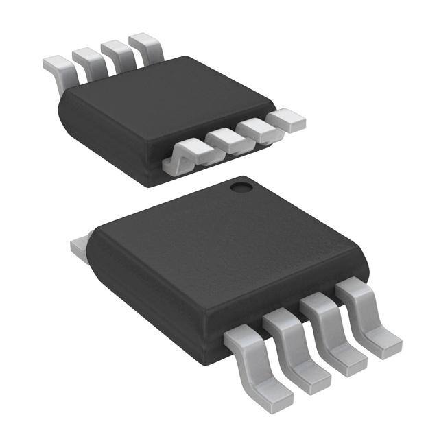
| 描述 | IC XLATR TTL-DIFF PECL 5V 8VSSOP转换 - 电压电平 5V PECL to TTL Translator |
| 产品分类 | 逻辑 - 变换器集成电路 - IC |
| 品牌 | Texas Instruments |
| 产品手册 | |
| 产品图片 |
|
| rohs | 符合RoHS无铅 / 符合限制有害物质指令(RoHS)规范要求 |
| 产品系列 | 逻辑集成电路,转换 - 电压电平,Texas Instruments SN65ELT21DGK65ELT |
| 数据手册 | |
| 产品型号 | SN65ELT21DGK |
| 产品目录页面 | |
| 产品种类 | 转换 - 电压电平 |
| 传播延迟(最大值) | 4.5ns |
| 位数 | 1 |
| 供应商器件封装 | 8-VSSOP |
| 其它名称 | 296-24936-5 |
| 包装 | 管件 |
| 商标 | Texas Instruments |
| 安装类型 | 表面贴装 |
| 安装风格 | SMD/SMT |
| 封装 | Tube |
| 封装/外壳 | 8-TSSOP,8-MSOP(0.118",3.00mm 宽) |
| 封装/箱体 | VSSOP-8 |
| 工作温度 | -40°C ~ 85°C |
| 工厂包装数量 | 80 |
| 差分-输入:输出 | 是/无 |
| 数据速率 | - |
| 最大工作温度 | + 85 C |
| 最小工作温度 | - 40 C |
| 标准包装 | 80 |
| 电压-电源 | 4.2 V ~ 5.7 V |
| 类型 | PECL to TTL |
| 系列 | SN65ELT21 |
| 输入类型 | PECL |
| 输出/通道数 | 1 |
| 输出类型 | TTL |
| 通道数 | 1 |
| 逻辑功能 | 变换器 |


- 商务部:美国ITC正式对集成电路等产品启动337调查
- 曝三星4nm工艺存在良率问题 高通将骁龙8 Gen1或转产台积电
- 太阳诱电将投资9.5亿元在常州建新厂生产MLCC 预计2023年完工
- 英特尔发布欧洲新工厂建设计划 深化IDM 2.0 战略
- 台积电先进制程称霸业界 有大客户加持明年业绩稳了
- 达到5530亿美元!SIA预计今年全球半导体销售额将创下新高
- 英特尔拟将自动驾驶子公司Mobileye上市 估值或超500亿美元
- 三星加码芯片和SET,合并消费电子和移动部门,撤换高东真等 CEO
- 三星电子宣布重大人事变动 还合并消费电子和移动部门
- 海关总署:前11个月进口集成电路产品价值2.52万亿元 增长14.8%


PDF Datasheet 数据手册内容提取
SN65ELT21 www.ti.com....................................................................................................................................................................................................... SLLS923–JUNE2009 5-V PECL-to-TTL Translator FEATURES 1 • 3ns(TYP)PropagationDelay PIN ASSIGNMENT • OperatingRange:V =4.2Vto5.7Vwith CC DorDGKPACKAGE GND=0V (TOPVIEW) • 24-mATTLOutput • DeterministicOutputValueforOpenInput NC 1 8 VCC ConditionsorWhenInputs<1.3V • Built-InTemperatureCompensation • Drop-InCompatibletotheMC10ELT21, D 2 7 Q MC100ELT21 D 3 6 NC APPLICATIONS • DataandClockTransmissionOverBackplane • SignalingLevelConversionforClockorData VBB 4 5 GND DESCRIPTION The SN65ELT21 is a differential PECL-to-TTL Table1.PinDescriptions translator. It operates on +5-V supply and ground PIN FUNCTION only. The device includes circuitry to maintain Q to a D,D PECLdatainputs low logic level when inputs are in an open condition or<1.3V. Q TTLoutput V Positivesupply The V pin is a reference voltage output for the CC BB device. When the device is used in single-ended VEE Negativesupply mode, the unused input should be tied to VBB. This VBB Referencevoltageoutput reference voltage can also be used to bias the input when it is ac coupled. When it is used, place a 0.01m F decoupling capacitor between V and V . CC BB Also limit the sink/source current to < 0.5 mA to V . BB LeaveV openwhenitisnotused. BB The SN65ELT21 is housed in an industry standard SOIC-8 package and is also available in an optional TSSOP-8package. ORDERINGINFORMATION(1)(2) PARTNUMBER PARTMARKING PACKAGE LEADFINISH SN65ELT21D ELT21 SOIC NiPdAu SN65ELT21DGK SIII SOIC-TSSOP NiPdAu (1) Forthemostcurrentpackageandorderinginformation,seethePackageOptionAddendumattheendofthisdocument,orseetheTI websiteatwww.ti.com. (2) Leadeddeviceoptionsarenotinitiallyavailable;contactasalesrepresentativeforfurtherdetails. 1 Pleasebeawarethatanimportantnoticeconcerningavailability,standardwarranty,anduseincriticalapplicationsofTexas Instrumentssemiconductorproductsanddisclaimerstheretoappearsattheendofthisdatasheet. PRODUCTIONDATAinformationiscurrentasofpublicationdate. Copyright©2009,TexasInstrumentsIncorporated Products conform to specifications per the terms of the Texas Instruments standard warranty. Production processing does not necessarilyincludetestingofallparameters.
SN65ELT21 SLLS923–JUNE2009....................................................................................................................................................................................................... www.ti.com Thesedeviceshavelimitedbuilt-inESDprotection.Theleadsshouldbeshortedtogetherorthedeviceplacedinconductivefoam duringstorageorhandlingtopreventelectrostaticdamagetotheMOSgates. ABSOLUTE MAXIMUM RATINGS(1) PARAMETER CONDITIONS VALUE UNIT AbsolutePECLmodesupplyvoltage V (GND=0V) 6 V CC Sink/sourcecurrent,V ±0.5 mA BB PECLinputvoltage GND=0V,V ≤V 6 V I CC Operatingtemperaturerange –40to85 °C Storagetemperaturerange –65to150 °C (1) Stressesbeyondthoselistedunderabsolutemaximumratingsmaycausepermanentdamagetothedevice.Thesearestressratings onlyandfunctionaloperationofthedeviceattheseoranyconditionsbeyondthoseindicatedunderrecommendedoperatingconditions isnotimplied.Exposuretoabsolute-maximum-ratedconditionsforextendedperiodsmayaffectdevicereliability. DISSIPATION RATINGS POWERRATING THERMALRESISTANCE, DERATINGFACTOR POWERRATING CIRCUITBOARD PACKAGE T <25°C JUNCTION-TO-AMBIENT T >25°C T =85°C MODEL A A A (mW) NOAIRFLOW (mW/°C) (mW) SOIC Low-K 719 139 7 288 High-K 840 119 8 336 SOIC-TSSOP Low-K 469 213 5 188 High-K 527 189 5 211 THERMAL CHARACTERISTICS overoperatingfree-airtemperaturerange(unlessotherwisenoted) PARAMETER MIN TYP MAX UNIT q Junction-to-boardthermalresistance SOIC 79 °C/W JB SOIC-TSSOP 120 q Junction-to-casethermalresistance SOIC 98 °C/W JC SOIC-TSSOP 74 KEY ATTRIBUTES CHARACTERISTICS VALUE Internalinputpull-downresistor 50kΩ Moisturesensitivitylevel Level1 Flameabilityrating(oxygenindex:28to34) UL94V-0at0.125in Electrostaticdischarge Humanbodymodel 2kV Charged-devicemodel 1.5kV MeetsorexceedsJEDECSpecEIA/JESD78latchuptest 2 SubmitDocumentationFeedback Copyright©2009,TexasInstrumentsIncorporated ProductFolderLink(s):SN65ELT21
SN65ELT21 www.ti.com....................................................................................................................................................................................................... SLLS923–JUNE2009 PECL DC CHARACTERISTICS AtV =5.0V,GND=0.0V(unlessotherwisenoted)(1)(2) CC T =–40°C T =25°C T =85°C A A A PARAMETER TESTCONDITIONS UNIT MIN TYP MAX MIN TYP MAX MIN TYP MAX V High-levelinputvoltage, 3835 4120 3835 4120 3835 4120 mV IH single-ended V Low-leveIinputvoltage, 3190 3525 3190 3525 3190 3525 mV IL single-ended V Outputreferencevoltage 3.62 3.69 3.74 3.62 3.69 3.74 3.62 3.69 3.74 V BB V High-levelinputvoltage, See (3) 2.2 5.0 2.2 5.0 2.2 5.0 V IHCMR common-moderange, differential I High-levelinputcurrent 150 150 150 m A IH I Low-levelinputcurrent 0.5 0.5 0.5 m A IL (1) Thedevicewillmeetthespecificationsafterthermalbalancehasbeenestablishedwhenmountedinasocketorprintedcircuitboard withmaintainedtransverseairflowgreaterthan500lfpm.Electricalparametersareassuredonlyoverthedeclaredoperating temperaturerange.Functionaloperationofthedeviceexceedingtheseconditionsisnotimplied.Devicespecificationlimitvaluesare appliedindividuallyundernormaloperatingconditionsandnotvalidsimultaneously. (2) Inputparametersvary1:1withV .V canvary+0.7V/–0.8V. CC CC (3) V varies1:1withGND,V varies1:1withV . IHCMR(min) IHCMR(max) CC TTL DC CHARACTERISTICS AtV =4.2Vto5.7V,T =–40°Cto85°C(unlessotherwisenoted)(1) CC A PARAMETER TESTCONDITIONS MIN TYP MAX UNIT I Powersupplycurrent 20 mA CCH I Powersupplycurrent 20 mA CCL V High-leveloutputvoltage I =–3.0mA 2.4 See (2) V OH OH V Low-leveloutputvoltage I =24mA 0.5 V OL OL I Outputshortcircuitcurrent –150 –60 mA OS (1) Thedevicewillmeetthespecificationsafterthermalbalancehasbeenestablishedwhenmountedinasocketorprintedcircuitboard withmaintainedtransverseairflowgreaterthan500lfpm.Electricalparametersareassuredonlyoverthedeclaredoperating temperaturerange.Functionaloperationofthedeviceexceedingtheseconditionsisnotimplied.Devicespecificationlimitvaluesare appliedindividuallyundernormaloperatingconditionsandnotvalidsimultaneously. (2) V isV –0.7. OH(max)level CC AC CHARACTERISTICS AtV =4.2Vto5.7V,GND=0.0V(unlessotherwisenoted)(1)(2) CC TEST TA=–40°C TA=25°C TA=85°C PARAMETER UNIT CONDITIONS MIN TYP MAX MIN TYP MAX MIN TYP MAX f Maximumswitching AtVol<0.5V 200 200 200 MHz MAX frequency (SeeFigure4) t /t Propagationdelaytimes At1.5V 2 4.5 2 4.5 2 4.5 ns PLH PHL t Randomclockjitter(RMS) 5 20 5 20 5 20 ps JITTER V Inputswing See (3) 200 1000 200 1000 200 1000 mV PP t/t Outputrise/falltimes Q(10%–90%) 750 780 910 ps r f (1) Thedevicewillmeetthespecificationsafterthermalequilibriumhasbeenestablishedwhenmountedinatestsocketorprintedcircuit boardwithmaintainedtransverseairflowgreaterthan500lfpm.Electricalparametersareassuredonlyoverthedeclaredoperating temperaturerange.Functionaloperationofthedeviceexceedingtheseconditionsisnotimplied.Devicespecificationlimitvaluesare appliedindividuallyundernormaloperatingconditionsandnotvalidsimultaneously. (2) R =500ΩtoGNDandC =20pFtoGND.SeeFigure1. L L (3) V isminimuminputswingforwhichacparametersareassured. PP(min) Copyright©2009,TexasInstrumentsIncorporated SubmitDocumentationFeedback 3 ProductFolderLink(s):SN65ELT21
SN65ELT21 SLLS923–JUNE2009....................................................................................................................................................................................................... www.ti.com TTLOutput C R C IncludesTest L L L Fixture Capacitance AC Test Load GND Figure1.TTLOutputACTestLoadingCondition IN IN 1.5 V 1.5 V OUT t t PLH PHL Figure2.OutputPropagationDelay 90% 10% t t r f Figure3.OutputRiseandFallTimes 4 SubmitDocumentationFeedback Copyright©2009,TexasInstrumentsIncorporated ProductFolderLink(s):SN65ELT21
SN65ELT21 www.ti.com....................................................................................................................................................................................................... SLLS923–JUNE2009 OUTPUTVOLTAGE vs FREQUENCY 5 VOH 85 4 V VOH 25 VOH -40 e - 3 g a olt VOL85 V put 2 VOL25 ut O VOL-40 1 V = 5.0V CC 0 0 50 100 150 200 250 300 350 400 450 500 Frequency - MHz Figure4. Copyright©2009,TexasInstrumentsIncorporated SubmitDocumentationFeedback 5 ProductFolderLink(s):SN65ELT21
PACKAGE OPTION ADDENDUM www.ti.com 6-Feb-2020 PACKAGING INFORMATION Orderable Device Status Package Type Package Pins Package Eco Plan Lead/Ball Finish MSL Peak Temp Op Temp (°C) Device Marking Samples (1) Drawing Qty (2) (6) (3) (4/5) SN65ELT21D ACTIVE SOIC D 8 75 Green (RoHS NIPDAU Level-1-260C-UNLIM -40 to 85 ELT21 & no Sb/Br) SN65ELT21DGK ACTIVE VSSOP DGK 8 80 Green (RoHS NIPDAU Level-1-260C-UNLIM -40 to 85 SIII & no Sb/Br) SN65ELT21DGKR ACTIVE VSSOP DGK 8 2500 Green (RoHS NIPDAU Level-1-260C-UNLIM -40 to 85 SIII & no Sb/Br) SN65ELT21DR ACTIVE SOIC D 8 2500 Green (RoHS NIPDAU Level-1-260C-UNLIM -40 to 85 ELT21 & no Sb/Br) (1) The marketing status values are defined as follows: ACTIVE: Product device recommended for new designs. LIFEBUY: TI has announced that the device will be discontinued, and a lifetime-buy period is in effect. NRND: Not recommended for new designs. Device is in production to support existing customers, but TI does not recommend using this part in a new design. PREVIEW: Device has been announced but is not in production. Samples may or may not be available. OBSOLETE: TI has discontinued the production of the device. (2) RoHS: TI defines "RoHS" to mean semiconductor products that are compliant with the current EU RoHS requirements for all 10 RoHS substances, including the requirement that RoHS substance do not exceed 0.1% by weight in homogeneous materials. Where designed to be soldered at high temperatures, "RoHS" products are suitable for use in specified lead-free processes. TI may reference these types of products as "Pb-Free". RoHS Exempt: TI defines "RoHS Exempt" to mean products that contain lead but are compliant with EU RoHS pursuant to a specific EU RoHS exemption. Green: TI defines "Green" to mean the content of Chlorine (Cl) and Bromine (Br) based flame retardants meet JS709B low halogen requirements of <=1000ppm threshold. Antimony trioxide based flame retardants must also meet the <=1000ppm threshold requirement. (3) MSL, Peak Temp. - The Moisture Sensitivity Level rating according to the JEDEC industry standard classifications, and peak solder temperature. (4) There may be additional marking, which relates to the logo, the lot trace code information, or the environmental category on the device. (5) Multiple Device Markings will be inside parentheses. Only one Device Marking contained in parentheses and separated by a "~" will appear on a device. If a line is indented then it is a continuation of the previous line and the two combined represent the entire Device Marking for that device. (6) Lead/Ball Finish - Orderable Devices may have multiple material finish options. Finish options are separated by a vertical ruled line. Lead/Ball Finish values may wrap to two lines if the finish value exceeds the maximum column width. Important Information and Disclaimer:The information provided on this page represents TI's knowledge and belief as of the date that it is provided. TI bases its knowledge and belief on information provided by third parties, and makes no representation or warranty as to the accuracy of such information. Efforts are underway to better integrate information from third parties. TI has taken and Addendum-Page 1
PACKAGE OPTION ADDENDUM www.ti.com 6-Feb-2020 continues to take reasonable steps to provide representative and accurate information but may not have conducted destructive testing or chemical analysis on incoming materials and chemicals. TI and TI suppliers consider certain information to be proprietary, and thus CAS numbers and other limited information may not be available for release. In no event shall TI's liability arising out of such information exceed the total purchase price of the TI part(s) at issue in this document sold by TI to Customer on an annual basis. Addendum-Page 2
PACKAGE MATERIALS INFORMATION www.ti.com 3-Aug-2017 TAPE AND REEL INFORMATION *Alldimensionsarenominal Device Package Package Pins SPQ Reel Reel A0 B0 K0 P1 W Pin1 Type Drawing Diameter Width (mm) (mm) (mm) (mm) (mm) Quadrant (mm) W1(mm) SN65ELT21DGKR VSSOP DGK 8 2500 330.0 12.4 5.3 3.4 1.4 8.0 12.0 Q1 SN65ELT21DR SOIC D 8 2500 330.0 12.4 6.4 5.2 2.1 8.0 12.0 Q1 PackMaterials-Page1
PACKAGE MATERIALS INFORMATION www.ti.com 3-Aug-2017 *Alldimensionsarenominal Device PackageType PackageDrawing Pins SPQ Length(mm) Width(mm) Height(mm) SN65ELT21DGKR VSSOP DGK 8 2500 367.0 367.0 35.0 SN65ELT21DR SOIC D 8 2500 367.0 367.0 35.0 PackMaterials-Page2
PACKAGE OUTLINE D0008A SOIC - 1.75 mm max height SCALE 2.800 SMALL OUTLINE INTEGRATED CIRCUIT C SEATING PLANE .228-.244 TYP [5.80-6.19] .004 [0.1] C A PIN 1 ID AREA 6X .050 [1.27] 8 1 2X .189-.197 [4.81-5.00] .150 NOTE 3 [3.81] 4X (0 -15 ) 4 5 8X .012-.020 B .150-.157 [0.31-0.51] .069 MAX [3.81-3.98] .010 [0.25] C A B [1.75] NOTE 4 .005-.010 TYP [0.13-0.25] 4X (0 -15 ) SEE DETAIL A .010 [0.25] .004-.010 0 - 8 [0.11-0.25] .016-.050 [0.41-1.27] DETAIL A (.041) TYPICAL [1.04] 4214825/C 02/2019 NOTES: 1. Linear dimensions are in inches [millimeters]. Dimensions in parenthesis are for reference only. Controlling dimensions are in inches. Dimensioning and tolerancing per ASME Y14.5M. 2. This drawing is subject to change without notice. 3. This dimension does not include mold flash, protrusions, or gate burrs. Mold flash, protrusions, or gate burrs shall not exceed .006 [0.15] per side. 4. This dimension does not include interlead flash. 5. Reference JEDEC registration MS-012, variation AA. www.ti.com
EXAMPLE BOARD LAYOUT D0008A SOIC - 1.75 mm max height SMALL OUTLINE INTEGRATED CIRCUIT 8X (.061 ) [1.55] SYMM SEE DETAILS 1 8 8X (.024) [0.6] SYMM (R.002 ) TYP [0.05] 5 4 6X (.050 ) [1.27] (.213) [5.4] LAND PATTERN EXAMPLE EXPOSED METAL SHOWN SCALE:8X SOLDER MASK SOLDER MASK METAL OPENING OPENING METAL UNDER SOLDER MASK EXPOSED METAL EXPOSED METAL .0028 MAX .0028 MIN [0.07] [0.07] ALL AROUND ALL AROUND NON SOLDER MASK SOLDER MASK DEFINED DEFINED SOLDER MASK DETAILS 4214825/C 02/2019 NOTES: (continued) 6. Publication IPC-7351 may have alternate designs. 7. Solder mask tolerances between and around signal pads can vary based on board fabrication site. www.ti.com
EXAMPLE STENCIL DESIGN D0008A SOIC - 1.75 mm max height SMALL OUTLINE INTEGRATED CIRCUIT 8X (.061 ) [1.55] SYMM 1 8 8X (.024) [0.6] SYMM (R.002 ) TYP [0.05] 5 4 6X (.050 ) [1.27] (.213) [5.4] SOLDER PASTE EXAMPLE BASED ON .005 INCH [0.125 MM] THICK STENCIL SCALE:8X 4214825/C 02/2019 NOTES: (continued) 8. Laser cutting apertures with trapezoidal walls and rounded corners may offer better paste release. IPC-7525 may have alternate design recommendations. 9. Board assembly site may have different recommendations for stencil design. www.ti.com
None
None
IMPORTANTNOTICEANDDISCLAIMER TI PROVIDES TECHNICAL AND RELIABILITY DATA (INCLUDING DATASHEETS), DESIGN RESOURCES (INCLUDING REFERENCE DESIGNS), APPLICATION OR OTHER DESIGN ADVICE, WEB TOOLS, SAFETY INFORMATION, AND OTHER RESOURCES “AS IS” AND WITH ALL FAULTS, AND DISCLAIMS ALL WARRANTIES, EXPRESS AND IMPLIED, INCLUDING WITHOUT LIMITATION ANY IMPLIED WARRANTIES OF MERCHANTABILITY, FITNESS FOR A PARTICULAR PURPOSE OR NON-INFRINGEMENT OF THIRD PARTY INTELLECTUAL PROPERTY RIGHTS. These resources are intended for skilled developers designing with TI products. You are solely responsible for (1) selecting the appropriate TI products for your application, (2) designing, validating and testing your application, and (3) ensuring your application meets applicable standards, and any other safety, security, or other requirements. These resources are subject to change without notice. TI grants you permission to use these resources only for development of an application that uses the TI products described in the resource. Other reproduction and display of these resources is prohibited. No license is granted to any other TI intellectual property right or to any third party intellectual property right. TI disclaims responsibility for, and you will fully indemnify TI and its representatives against, any claims, damages, costs, losses, and liabilities arising out of your use of these resources. TI’s products are provided subject to TI’s Terms of Sale (www.ti.com/legal/termsofsale.html) or other applicable terms available either on ti.com or provided in conjunction with such TI products. TI’s provision of these resources does not expand or otherwise alter TI’s applicable warranties or warranty disclaimers for TI products. Mailing Address: Texas Instruments, Post Office Box 655303, Dallas, Texas 75265 Copyright © 2020, Texas Instruments Incorporated