 Datasheet下载
- 型号: SMP100LC-160
- 制造商: STMicroelectronics
- 库位|库存: xxxx|xxxx
- 要求:
| 数量阶梯 | 香港交货 | 国内含税 |
| +xxxx | $xxxx | ¥xxxx |
查看当月历史价格
查看今年历史价格
SMP100LC-160产品简介:
ICGOO电子元器件商城为您提供SMP100LC-160由STMicroelectronics设计生产,在icgoo商城现货销售,并且可以通过原厂、代理商等渠道进行代购。 SMP100LC-160价格参考。STMicroelectronicsSMP100LC-160封装/规格:TVS - 晶闸管, 160V Off-State 400A Ipp TVS Thyristor DO-214AA,SMB。您可以下载SMP100LC-160参考资料、Datasheet数据手册功能说明书,资料中有SMP100LC-160 详细功能的应用电路图电压和使用方法及教程。
STMicroelectronics的SMP100LC-160是一款属于TVS(瞬态电压抑制)类别的晶闸管,主要用于保护电子电路免受高电压瞬态干扰的损害。该器件具有较高的浪涌电流承受能力和快速响应特性,适用于需要高可靠性和高耐压保护的场合。

其主要应用场景包括:

1. 电力电子设备保护:用于交流电源输入端,防止雷击、电感负载切换等引起的高电压浪涌对后级电路造成损坏。

2. 工业控制系统:在PLC、变频器、伺服系统等工业设备中,作为过压保护元件,保障控制电路稳定运行。

3. 家电产品:如空调、洗衣机、电磁炉等大功率家电中,用于保护电源模块和控制电路免受电网瞬态干扰。

4. 智能电网与能源系统:应用于智能电表、太阳能逆变器等设备中,提供线路过压和静电放电(ESD)保护。

5. 汽车电子:在车载充电系统、电池管理系统(BMS)等中,用于抵御车辆电源系统中可能产生的电压尖峰。

SMP100LC-160因其高浪涌容量和良好的钳位特性,特别适合用于需要频繁承受较大瞬态能量冲击的应用环境。
| 参数 | 数值 |
| 产品目录 | |
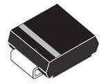
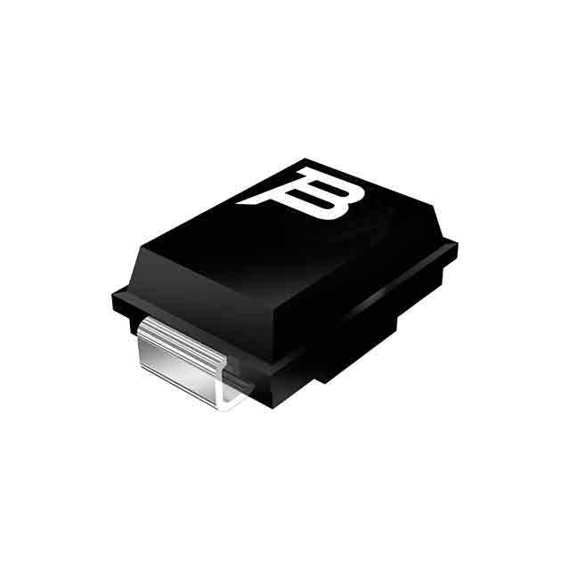
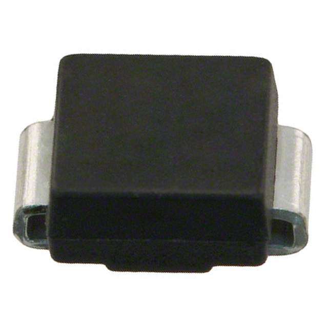
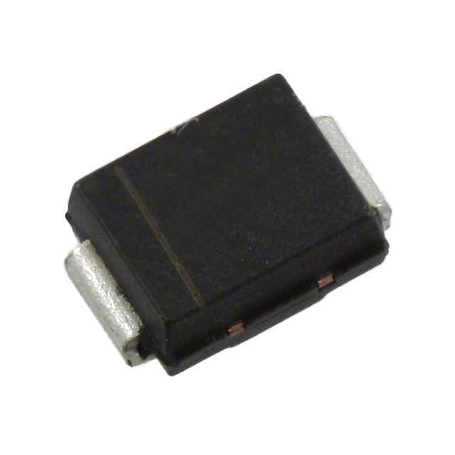
| 描述 | TRISIL 100A 160V BIDIRECT SMBTVS 二极管 - 瞬态电压抑制器 160V 50uA Bidirect |
| 产品分类 | |
| 品牌 | STMicroelectronics |
| 产品手册 | |
| 产品图片 |
|
| rohs | 符合RoHS无铅 / 符合限制有害物质指令(RoHS)规范要求 |
| 产品系列 | 二极管与整流器,TVS二极管,TVS 二极管 - 瞬态电压抑制器,STMicroelectronics SMP100LC-160SMP, TRISIL™ |
| 数据手册 | |
| 产品型号 | SMP100LC-160 |
| 产品目录页面 | |
| 产品种类 | TVS 二极管 - 瞬态电压抑制器 |
| 元件数 | 1 |
| 其它名称 | 497-4089-1 |
| 其它有关文件 | http://www.st.com/web/catalog/sense_power/FM114/CL1802/SC496/PF64220?referrer=70071840 |
| 击穿电压 | 160 V |
| 包装 | 剪切带 (CT) |
| 单位重量 | 110 mg |
| 商标 | STMicroelectronics |
| 安装风格 | SMD/SMT |
| 封装 | Reel |
| 封装/外壳 | DO-214AA,SMB |
| 封装/箱体 | DO-214AA |
| 尺寸 | 5.6 mm W x 4.6 mm L x 2.45 mm H |
| 峰值浪涌电流 | 100 A |
| 工作电压 | 144 V |
| 工厂包装数量 | 2500 |
| 最大工作温度 | + 150 C |
| 最小工作温度 | - 40 C |
| 极性 | Bidirectional |
| 标准包装 | 1 |
| 电压-导通 | 200V |
| 电压-断态 | 160V |
| 电压-通态 | - |
| 电容 | 30 pF |
| 电流-保持(Ih) | 150mA |
| 电流-峰值脉冲(10/1000µs) | 100A |
| 电流-峰值脉冲(8/20µs) | 400A |
| 端接类型 | SMD/SMT |
| 系列 | SMP100LC |


- 商务部:美国ITC正式对集成电路等产品启动337调查
- 曝三星4nm工艺存在良率问题 高通将骁龙8 Gen1或转产台积电
- 太阳诱电将投资9.5亿元在常州建新厂生产MLCC 预计2023年完工
- 英特尔发布欧洲新工厂建设计划 深化IDM 2.0 战略
- 台积电先进制程称霸业界 有大客户加持明年业绩稳了
- 达到5530亿美元!SIA预计今年全球半导体销售额将创下新高
- 英特尔拟将自动驾驶子公司Mobileye上市 估值或超500亿美元
- 三星加码芯片和SET,合并消费电子和移动部门,撤换高东真等 CEO
- 三星电子宣布重大人事变动 还合并消费电子和移动部门
- 海关总署:前11个月进口集成电路产品价值2.52万亿元 增长14.8%


PDF Datasheet 数据手册内容提取
SMP100LC Trisil™ for telecom equipment protection Features ■ Bidirectional crowbar protection ■ Voltage range from 8 V to 400 V ■ Low capacitance from 20 pF to 45 pF @ 2 V ■ Low leakage current: I = 2 µA max R SMB ■ Holding current: I = 150 mA min. (JEDEC DO-214AA) H ■ Repetitive peak pulse current: I = 100 A (10/1000 µs) PP Benefits ■ Trisils are not subject to ageing and provide a fail safe mode in short circuit for better protection. ■ Helps equipment meet main standards such as UL60950, IEC 950 / CSA C22.2 and UL1459. ■ Epoxy meets UL94, V0. Description ■ Package is JEDEC registered (DO-214AA). The SMP100LC is a series of low capacitance Complies with the following standards transient surge arrestors designed for the protection of high data rate communication ■ GR-1089 Core equipment. The low capacitance of the devices ■ ITU-T-K20/K21 avoids any distortion of the signal and is compatible with digital transmission line cards ■ IEC 61000-4-5 (xDSL, ISDN...). ■ IEC 61000-4-2 level 4 SMP100LC series tested and confirmed ■ TIA/EIA IS-968 compatible with Cooper Bussmann Telecom ■ UL497B recognized, UL file E136224 Circuit Protector TCP 1.25A. The SMP100LC-xxx with the fuse TCP1.25A or Applications TCP2A is compliant with Telcordia GR1089 (lightning and AC power fault tests), Any sensitive equipment requiring protection ITU-TK20/K21 (lightning and AC power fault against lightning strikes and AC power faults. tests), TIA/EIA-IS-968 (formerly FCC Part 68 These devices are dedicated to central office lightning tests), and UL60950 (AC power fault protection as they comply with the most stressful tests). The use of the TCP1.25A allows the standards. Their low capacitances make them SMP100LC-xxx to be safe for the 2nd level (B suitable for xDSL. criteria) AC power fault tests. TM: Trisil is a trademark of STMicroelectronics February 2012 Doc ID 7050 Rev 14 1/13 www.st.com 13
Characteristics SMP100LC 1 Characteristics T able 1. In compliance with the following standards Peak surge Required Minimum serial Waveform Current Standard voltage peak current resistor to meet voltage waveform (V) (A) standard (Ω) GR-1089 Core 2500 2/10 µs 500 2/10 µs 0 First level 1000 10/1000 µs 100 10/1000 µs 0 GR-1089 Core 5000 2/10 µs 500 2/10 µs 0 Second level GR-1089 Core 1500 2/10 µs 100 2/10 µs 0 Intra-building 6000 150 0 ITU-T-K20/K21 10/700 µs 5/310 µs 1500 37.5 0 ITU-T-K20 8000 ESD contact discharge 0 1/60 ns (IEC61000-4-2) 15000 ESD air discharge 0 4000 10/700 µs 100 5/310 µs 0 IEC61000-4-5 4000 1.2/50 µs 100 8/20 µs 0 TIA/EIA IS-968, 1500 10/160 µs 200 10/160 µs 0 lightning surge type A 800 10/560 µs 100 10/560 µs 0 TIA/EIA IS-968, 1000 9/720 µs 25 5/320 µs 0 lightning surge type B 2/13 Doc ID 7050 Rev 14
SMP100LC Characteristics T able 2. Absolute ratings (T = 25 °C) amb Symbol Parameter Value Unit 10/1000 µs 100 8/20 µs 400 10/560 µs 140 I Repetitive peak pulse current (see Figure2) 5/310 µs 150 A PP 10/160 µs 200 1/20 µs 400 2/10 µs 500 I Fail-safe mode: maximum current (1) 8/20 µs 5 kA FS t = 0.2 s 24 Non repetitive surge peak on-state current t = 1 s 15 I A TSM (sinusoidal) t = 2 s 12 t = 15 mn 4 t = 16.6 ms 20 I2t I2t value for fusing A2s t = 20 ms 21 T Storage temperature range -55 to 150 stg °C T Operating junction temperature range -40 to 150 j T Maximum lead temperature for soldering during 10 s. 260 °C L 1. In fail safe mode, the device acts as a short circuit. T able 3. Thermal resistances Symbol Parameter Value Unit R Junction to ambient (with recommended footprint) 100 °C/W th(j-a) R Junction to leads 20 °C/W th(j-l) Figure 1. Electrical characteristics - definitions (T = 25 °C) amb Symbol Parameter I I PP V Stand-off voltage RM V Breakover voltage BO I Leakage current RM I I Peak pulse current BO PP I I Breakover current H BO IH Holding current IRM V V Continuous reverse voltage R V V V I Leakage current atV RM R BO R R C Capacitance Doc ID 7050 Rev 14 3/13
Characteristics SMP100LC T able 4. Electrical characteristics - values (T = 25 °C) amb Dynamic Static I @ V I @ V I (3) C(4) C(5) RM RM R R V (1) V @ I (2) H BO BO BO Order code max. max. max. max. max. min. typ. typ. µA V µA V V V mA mA pF pF 50 SMP100LC-8 6 8 25 15 NA 75 (typ.) SMP100LC-25 22 25 40 35 NA 65 SMP100LC-35 32 35 55 55 NA 55 SMP100LC-65 55 65 85 85 45 90 SMP100LC-90 81 90 120 125 40 80 SMP100LC-120 108 120 155 150 35 75 SMP100LC-140 2 126 5 140 180 175 800 30 65 150 SMP100LC-160 144 160 205 200 30 65 SMP100LC-200 180 200 255 250 30 60 SMP100LC-230 207 230 295 285 30 60 SMP100LC-270 243 270 345 335 30 60 SMP100LC-320 290 320 400 390 25 50 SMP100LC-360 325 360 460 450 25 50 SMP100LC-400 360 400 540 530 20 45 1. See Figure16: Test circuit 1 for Dynamic I and V parameters BO BO 2. See Figure17: Test circuit 2 for I and V parameters BO BO 3. See Figure18: Test circuit 3 for dynamic I parameter H 4. V = 50 V bias, V =1 V, F = 1 MHz R RMS 5. V = 2V bias, V =1 V, F = 1 MHz R RMS 4/13 Doc ID 7050 Rev 14
SMP100LC Characteristics Figure 2. P ulse waveform Figure 3. Non repetitive surge peak on-state current versus overload duration %IPP Repetitive peak pulse current ITSM(A) tr = rise time (µs) 70 F=50Hz 100 tp = pulse duration time (µs) 60 Tjinitial = 25°C 50 40 50 30 20 10 0 t t(s) tr tp 0 1E-2 1E-1 1E+0 1E+1 1E+2 1E+3 Figure 4. O n-state voltage versus on-state Figure 5. Relative variation of holding current (typical values) current versus junction temperature IT(A) IH[Tj] / IH[Tj=25°C] 100 2.0 Tjinitial = 25°C 1.8 1.6 1.4 1.2 1.0 0.8 0.6 0.4 VT(V) 0.2 Tj(°C) 0.0 10 -25 0 25 50 75 100 125 0 1 2 3 4 5 6 7 8 Figure 6. R elative variation of breakover Figure 7. Relative variation of leakage voltage versus junction current versus junction temperature temperature (typical values) VBO[Tj] /VBO[Tj=25°C] IR[Tj] / IR[Tj=25°C] 1.08 2000 1000 1.06 1.04 100 1.02 1.00 10 0.98 Tj(°C) Tj(°C) 0.96 1 -25 0 25 50 75 100 125 25 50 75 100 125 Doc ID 7050 Rev 14 5/13
Application information SMP100LC Figure 8. V ariation of thermal impedance Figure 9. Relative variation of junction junction to ambient versus pulse capacitance versus reverse voltage duration applied (typical values) Zth(j-a)/Rth(j-a) C [VR] / C [VR=2V] 1 1.4 Printed circuit board - FR4, F =1MHz copper thickness = 35µm, 1.2 VTRjM=S 2=5 °1CV recommended pad layout 1.0 0.8 0.1 0.6 0.4 0.2 tp(s) VR(V) 0.01 0.0 1E-3 1E-2 1E-1 1E+0 1E+1 1E+2 5E+2 1 2 5 10 20 50 100 300 2 Application information In wire line applications, analog or digital, both central office and subscriber sides have to be protected. This function is assumed by a combined series / parallel protection stage. Figure 10. Examples of protection stages for line cards Ring relay e e g g a a Line on st Line on st ecti ecti ot ot Pr Pr Ex.Analog line card Ex.xDSL line card or terminal In such a stage, parallel function is assumed by one or several Trisil, and is used to protect against short duration surge (lightning). During this kind of surges the Trisil limits the voltage across the device to be protected at its break over value and then fires. The fuse assumes the series function, and is used to protect the module against long duration or very high current mains disturbances (50/60Hz). It acts by safe circuit opening. Lightning surge and mains disturbance surges are defined by standards like GR1089, TIA/EIA IS-968, ITU-TK20. Figure 11. Typical circuits FuseTCP 1.25A Tip L Tip S FuseTCP 1.25A T1 SMP100LC-xxx SMP100LC-xxx Gnd Gnd T2 SMP100LC-xxx FuseTCP 1.25A Ring L Ring S Typical circuit for subscriber side Typical circuit for central office side 6/13 Doc ID 7050 Rev 14
SMP100LC Application information Figure 12. Test method of the board with fuse and Trisil I surge Surge Device to be protected Generator Test board Line side V Oscilloscope Current probe Voltage probe These topologies, using SMP100LC from ST and TCP1.25A from Cooper Bussmann, have been functionally validated with a Trisil glued on the PCB. Following example was performed with SMP100LC-270 Trisil. For more information, see Application Note AN2064. Figure 13. Trisil turns on during lightning strike I surge (100A/div) V (50V/div) Test conditions: 2/10 µs + and - 2.5 and 5 kV, 500 A (10 pulses of each polarity), T = 25 °C amb Test result: Fuse and Trisil OK after test in accordance with GR1089 requirements. Doc ID 7050 Rev 14 7/13
Application information SMP100LC Figure 14. Trisil action while fuse remains operational I surge (2A/div) V (100V/div) Test conditions: 600 V, 3 A, 1.1 s (first level), T = 25 °C amb Test result: Fuse and Trisil OK after test in accordance with GR1089 requirements. Figure 15. High current AC power test: the fuse acts like a switch by opening the circuit I surge (10A/div) V (100V/div) Test conditions: 277 V, 25 A (second level), T = 25 °C amb Test result: Fuse safely opened and Trisil OK after test in accordance with GR1089 requirements. 8/13 Doc ID 7050 Rev 14
SMP100LC Application information Figure 16. Test circuit 1 for Dynamic I and V parameters BO BO 100V/µs, di/dt<10A/µs, Ipp=100A 2Ω 45Ω 83Ω 46 µH 10 µF 0.36 nF U 66Ω 470Ω KeyTek'System2' generatorwithPN246I module 1kV/µs, di/dt<10A/µs,Ipp=10A 26µH 250Ω 47Ω 46 µH U 60 µF 12Ω KeyTek'System2' generatorwithPN246I module Figure 17. Test circuit 2 for I and V parameters BO BO K ton = 20ms R1 = 140Ω R2 = 240Ω 220V 50Hz Vout DUT measVuBrOement 1/4 IBO measurement TEST PROCEDURE Pulse test duration (tp = 20ms): ● for Bidirectional devices = Switch K is closed ● for Unidirectional devices = Switch K is open VOUTselection: ● Device withVBO< 200V➔ VOUT= 250VRMS, R1 = 140Ω ● Device withVBO≥200V➔ VOUT= 480VRMS, R2 = 240Ω Doc ID 7050 Rev 14 9/13
Ordering information scheme SMP100LC Figure 18. Test circuit 3 for dynamic I parameter H R Surge generator V =-48V D.U.T BAT This is a GO-NOGO test which allows to confirm the holding current (IH) level in a functional test circuit. TEST PROCEDURE 1/ Adjust the current level at the IHvalue by short circuiting the AK of the D.U.T. 2/ Fire the D.U.T.with a surge current ➔ IPP=10A,10/1000µs. 3/The D.U.T.will come back off-state within 50ms maximum. 3 Ordering information scheme Figure 19. Ordering information scheme SMP 100 LC - xxx Trisil surface mount Repetitive peak pulse current 100 = 100 A Capacitance LC = Low capacitance Voltage 65 = 65V 10/13 Doc ID 7050 Rev 14
SMP100LC Package information 4 Package information ● Epoxy meets UL94, V0 ● Lead-free package In order to meet environmental requirements, ST offers these devices in different grades of ECOPACK® packages, depending on their level of environmental compliance. ECOPACK® specifications, grade definitions and product status are available at: www.st.com. ECOPACK® is an ST trademark. T able 5. SMB dimensions Dimensions Ref. Millimeters Inches E1 Min. Max. Min. Max. A1 1.90 2.45 0.075 0.096 D A2 0.05 0.20 0.002 0.008 b 1.95 2.20 0.077 0.087 E c 0.15 0.40 0.006 0.016 A1 E 5.10 5.60 0.201 0.220 E1 4.05 4.60 0.159 0.181 C A2 L b D 3.30 3.95 0.130 0.156 L 0.75 1.50 0.030 0.059 F igure 20. Footprint dimensions Figure 21. Marking layout(1) in mm (inches) 1.62 2.60 1.62 (0.064) (0.102) (0.064) Cathode bar (unidirectional devices only) 2.18 e e:ECOPACK compliance XXX: Marking (0.086) x x x Z: Manufacturing location Y: Year WW: week z y ww 5.84 (0.23) 1. Marking layout can vary according to assembly location. Doc ID 7050 Rev 14 11/13
Ordering information SMP100LC 5 Ordering information T able 6. Ordering information Order code Marking Package Weight Base qty Delivery mode SMP100LC-8 PL8 SMP100LC-25 L25 SMP100LC-35 L35 SMP100LC-65 L06 SMP100LC-90 L09 SMP100LC-120 L12 SMP100LC-140 L14 SMB 98 mg 2500 Tape and reel SMP100LC-160 L16 SMP100LC-200 L20 SMP100LC-230 L23 SMP100LC-270 L27 SMP100LC-320 L32 SMP100LC-360 L36 SMP100LC-400 L40 6 Revision history T able 7. Document revision history Date Revision Changes 09-Nov-2004 9 Absolute ratings values, table 3 on page 2, updated. 07-Dec-2004 10 SMP100LC-320, SMP100LC-360 and SMP100LC-400 addition. 20-Jun-2005 11 Telecom Circuit Protector added in Description. Reformatted to current standards. SMB Package information 05-Mar-2007 12 updated. Standards compliance paragraphs added to Description. 05-Jan-2010 13 Corrected vertical axis labelling in Figure8. 09-Feb-2012 14 Added UL statement in Complies with the following standards. 12/13 Doc ID 7050 Rev 14
SMP100LC Please Read Carefully: Information in this document is provided solely in connection with ST products. STMicroelectronics NV and its subsidiaries (“ST”) reserve the right to make changes, corrections, modifications or improvements, to this document, and the products and services described herein at any time, without notice. All ST products are sold pursuant to ST’s terms and conditions of sale. Purchasers are solely responsible for the choice, selection and use of the ST products and services described herein, and ST assumes no liability whatsoever relating to the choice, selection or use of the ST products and services described herein. No license, express or implied, by estoppel or otherwise, to any intellectual property rights is granted under this document. If any part of this document refers to any third party products or services it shall not be deemed a license grant by ST for the use of such third party products or services, or any intellectual property contained therein or considered as a warranty covering the use in any manner whatsoever of such third party products or services or any intellectual property contained therein. UNLESS OTHERWISE SET FORTH IN ST’S TERMS AND CONDITIONS OF SALE ST DISCLAIMS ANY EXPRESS OR IMPLIED WARRANTY WITH RESPECT TO THE USE AND/OR SALE OF ST PRODUCTS INCLUDING WITHOUT LIMITATION IMPLIED WARRANTIES OF MERCHANTABILITY, FITNESS FOR A PARTICULAR PURPOSE (AND THEIR EQUIVALENTS UNDER THE LAWS OF ANY JURISDICTION), OR INFRINGEMENT OF ANY PATENT, COPYRIGHT OR OTHER INTELLECTUAL PROPERTY RIGHT. UNLESS EXPRESSLY APPROVED IN WRITING BY TWO AUTHORIZED ST REPRESENTATIVES, ST PRODUCTS ARE NOT RECOMMENDED, AUTHORIZED OR WARRANTED FOR USE IN MILITARY, AIR CRAFT, SPACE, LIFE SAVING, OR LIFE SUSTAINING APPLICATIONS, NOR IN PRODUCTS OR SYSTEMS WHERE FAILURE OR MALFUNCTION MAY RESULT IN PERSONAL INJURY, DEATH, OR SEVERE PROPERTY OR ENVIRONMENTAL DAMAGE. ST PRODUCTS WHICH ARE NOT SPECIFIED AS "AUTOMOTIVE GRADE" MAY ONLY BE USED IN AUTOMOTIVE APPLICATIONS AT USER’S OWN RISK. Resale of ST products with provisions different from the statements and/or technical features set forth in this document shall immediately void any warranty granted by ST for the ST product or service described herein and shall not create or extend in any manner whatsoever, any liability of ST. ST and the ST logo are trademarks or registered trademarks of ST in various countries. Information in this document supersedes and replaces all information previously supplied. The ST logo is a registered trademark of STMicroelectronics. All other names are the property of their respective owners. © 2012 STMicroelectronics - All rights reserved STMicroelectronics group of companies Australia - Belgium - Brazil - Canada - China - Czech Republic - Finland - France - Germany - Hong Kong - India - Israel - Italy - Japan - Malaysia - Malta - Morocco - Philippines - Singapore - Spain - Sweden - Switzerland - United Kingdom - United States of America www.st.com Doc ID 7050 Rev 14 13/13
Mouser Electronics Authorized Distributor Click to View Pricing, Inventory, Delivery & Lifecycle Information: S TMicroelectronics: SMP100LC-90 SMP100LC-65 SMP100LC-25 SMP100LC-400 SMP100LC-200 SMP100LC-160 SMP100LC-120 SMP100LC-230 SMP100LC-270 SMP100LC-140 SMP100LC-35 SMP100LC-360 SMP100LC-320 SMP100LC-8