 Datasheet下载
- 型号: SMAJ28A
- 制造商: Bourns
- 库位|库存: xxxx|xxxx
- 要求:
| 数量阶梯 | 香港交货 | 国内含税 |
| +xxxx | $xxxx | ¥xxxx |
查看当月历史价格
查看今年历史价格
SMAJ28A产品简介:
ICGOO电子元器件商城为您提供SMAJ28A由Bourns设计生产,在icgoo商城现货销售,并且可以通过原厂、代理商等渠道进行代购。 SMAJ28A价格参考。BournsSMAJ28A封装/规格:TVS - 二极管, 。您可以下载SMAJ28A参考资料、Datasheet数据手册功能说明书,资料中有SMAJ28A 详细功能的应用电路图电压和使用方法及教程。
Bourns Inc. 生产的型号为 SMAJ28A 的 TVS 二极管(瞬态电压抑制二极管)是一种用于电路保护的关键元件。其应用场景主要包括以下几个方面:

1. 电源线和信号线保护:SMAJ28A 可以有效保护电源线和信号线免受瞬态电压的影响,如雷击、静电放电(ESD)和其他电气干扰。它能够在短时间内吸收大量能量,确保电路中的其他敏感元件不会因过压而损坏。

2. 通信设备保护:在通信设备中,如电话、网络设备、调制解调器等,SMAJ28A 可以防止由于外界电磁干扰或线路故障引起的电压波动,确保数据传输的稳定性和可靠性。

3. 工业自动化系统:在工业环境中,各种传感器、控制器和执行器可能会受到来自电机启动、开关操作或其他设备产生的瞬态电压冲击。SMAJ28A 能够提供有效的保护,延长这些设备的使用寿命。

4. 汽车电子系统:现代汽车中的电子控制系统越来越多,如发动机管理、安全气囊、车载娱乐系统等。SMAJ28A 可以保护这些系统免受电池电压波动、发电机浪涌以及其他电气干扰的影响,确保车辆的安全性和性能。

5. 消费电子产品:在智能手机、平板电脑、笔记本电脑等消费电子产品中,SMAJ28A 可以保护内部电路免受外部环境中的静电放电和电压瞬变影响,提高产品的可靠性和用户体验。

6. 医疗设备:医疗设备对电路保护的要求非常高,因为任何故障都可能导致严重的后果。SMAJ28A 可以用于保护心电图机、超声波设备、监护仪等医疗设备中的关键电路,确保设备的正常运行和患者的安全。

总之,SMAJ28A TVS 二极管广泛应用于各种需要电路保护的场合,能够有效应对瞬态电压带来的潜在威胁,保障设备的稳定性和安全性。
| 参数 | 数值 |
| 产品目录 | |
| 描述 | TVS DIODE 28VWM SMDTVS 二极管 - 瞬态电压抑制器 28volts 5uA 8.8 Amps Uni-Dir |
| 产品分类 | |
| 品牌 | Bourns |
| 产品手册 | |
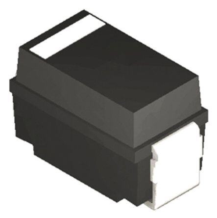
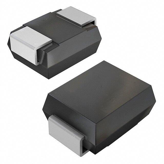
| 产品图片 |
|
| rohs | RoHS 合规性豁免不受无铅要求限制 / 符合限制有害物质指令(RoHS)规范要求 |
| 产品系列 | 二极管与整流器,TVS二极管,TVS 二极管 - 瞬态电压抑制器,Bourns SMAJ28ASMAJ |
| 数据手册 | |
| 产品型号 | SMAJ28A |
| RoHS指令信息 | |
| 不同频率时的电容 | - |
| 产品目录绘图 |
|
| 产品目录页面 | |
| 产品种类 | TVS 二极管 - 瞬态电压抑制器 |
| 供应商器件封装 | SMA (DO-214AC) |
| 其它名称 | SMAJ28ABDKR |
| 击穿电压 | 31.1 V to 34.4 V |
| 功率-峰值脉冲 | 400W |
| 包装 | Digi-Reel® |
| 单向通道 | 1 |
| 双向通道 | - |
| 商标 | Bourns |
| 安装类型 | 表面贴装 |
| 安装风格 | SMD/SMT |
| 封装 | Reel |
| 封装/外壳 | DO-214AC,SMA |
| 封装/箱体 | DO-214AC |
| 尺寸 | 2.92 mm W x 4.57 mm L x 2.62 mm H |
| 峰值浪涌电流 | 40 A |
| 峰值脉冲功率耗散 | 400 W |
| 工作温度 | -55°C ~ 150°C |
| 工作电压 | 3.5 V |
| 工厂包装数量 | 5000 |
| 应用 | 通用 |
| 最大工作温度 | + 150 C |
| 最小工作温度 | - 55 C |
| 极性 | Unidirectional |
| 标准包装 | 1 |
| 特色产品 | http://www.digikey.com/product-highlights/cn/zh/bourns-smx-tvs-diodes/1448 |
| 电压-击穿(最小值) | 31.1V |
| 电压-反向关态(典型值) | 28V |
| 电压-箝位(最大值)@Ipp | - |
| 电流-峰值脉冲(10/1000µs) | - |
| 电源线路保护 | 无 |
| 端接类型 | SMD/SMT |
| 类型 | 齐纳 |
| 系列 | SMAJ |


PDF Datasheet 数据手册内容提取
NT *RoHS VCEOARVMSIAPILOLINAASB LE Features Applications NT MPLIA n RoHS compliant* n IEC 61000-4-2 ESD (Min. Level 4) O HS C n Surface Mount SMA package n IEC 61000-4-4 EFT Ro * n Standoff Voltage: 5.0 to 495 volts n IEC 61000-4-5 Surge n Power Dissipation: 400 watts REE D F LEA SMAJ Transient Voltage Suppressor Diode Series General Information TiBnhoceure rmnassa irnokgfefeltysr s so mTf rapalonlerstrai eebnlleet c Vctrooolmtnaimgc euc onSmiucapptpoiornenessns,t oscLr.VoER EADomRDH SIiSF poORCNuEdOSE teMAiPnsRLIEg Af NoaTr*n sdu vrgidee aon edq EuiSpDm epnrot taercet iochna allpepnlgicinagtio tnhse, sine mcoicmopnadcutc ctohri pin pdaucsktrayg teo DdOev-e2l1o4pA C (SMA) size format. The Transient Voltage Suppressor series offers a choice of Working Peak Reverse Voltage from 5 V up to 495 V and Breakdown Voltage up to 550 V. Typical fast response times are less than 1.0 picoseconds for unidirectional devices and less than 5.0 picoseconds for bidirectional devices from 0 V to Minimum Breakdown Voltage. Bourns® Chip Diodes conform to JEDEC standards, are easy to handle with standard pick and place equipment and the flat configuration minimizes roll away. Electrical Characteristics (@ TA = 25 °C Unless Otherwise Noted) Parameter Symbol Value Unit Minimum Peak Pulse Power Dissipation (TP = 1 ms) (Note 1,2) PPK 400 Watts Peak Forward Surge Current 8.3 ms Single Half Sine Wave Superimposed on Rated Load IFSM 40 Amps (JEDEC Method) (Note 3) Steady State Power Dissipation @ TL = 75 °C PM(AV) 1.0 Watts M(Faoxr imUnuimdi rIencsttiaonntaal nUenoiutss OFnolryw)ard Voltage @ IPP = 35 A SSMMAAJJ51.000AA ~ ~ S SMMAAJJ9409A5 A VF 35..50 Volts Operating Temperature Range TJ -55 to +150 °C Storage Temperature Range TSTG -55 to +150 °C 1. Non-repetitive current pulse, per Pulse Waveform graph and derated above TA = 25 °C per Pulse Derating Curve. 2. Thermal Resistance Junction to Lead. 3. 8.3 ms Single Half-Sine Wave duty cycle = 4 pulses maximum per minute (unidirectional units only). How to Order SMAJ 5.0 CA - H Package SMAJ = SMA/DO-214AC Working Peak Reverse Voltage 5.0 = 5.0 VRWM (Volts) Suffix A = 5 % Tolerance Unidirectional Device Asia-Pacific: CA = 5 % Tolerance Bidirectional Device Tel: +886-2 2562-4117 Reel Email: asiacus@bourns.com (blank) = 13 inch reel -H = 7 inch reel Europe: Tel: +36 88 520 390 Email: eurocus@bourns.com The Americas: Tel: +1-951 781-5500 Email: americus@bourns.com www.bourns.com *RoHS Directive 2002/95/EC Jan. 27, 2003 including annex and RoHS Recast 2011/65/EU June 8, 2011. Specifications are subject to change without notice. The device characteristics and parameters in this data sheet can and do vary in different applications and actual device performance may vary over time. Users should verify actual device performance in their specific applications.
SMAJ Transient Voltage Suppressor Diode Series Electrical Characteristics (@ TA = 25 °C Unless Otherwise Noted) Working Maximum Maximum Maximum Breakdown Voltage Peak Reverse Reverse Reverse Unidirectional Device Bidirectional Device VBR (Volts) Reverse Leakage Voltage Surge Voltage @ VRWM @ IRSM Current Part No. Marking Part No. Marking Min. Max. @ IT (mA) VRWM (V) IR (μA) VRSM (V) IRSM (A) SMAJ5.0A HE SMAJ5.0CA TE 6.40 7.00 10 5.0 800 9.2 43.5 SMAJ6.0A HG SMAJ6.0CA TG 6.67 7.37 10 6.0 800 10.3 38.8 SMAJ6.5A HK SMAJ6.5CA TK 7.22 7.98 10 6.5 500 11.2 35.7 SMAJ7.0A HM SMAJ7.0CA TM 7.78 8.60 10 7.0 200 12.0 33.3 SMAJ7.5A HP SMAJ7.5CA TP 8.33 9.21 1.0 7.5 100 12.9 31.0 SMAJ8.0A HR SMAJ8.0CA TR 8.89 9.83 1.0 8.0 50 13.6 29.4 SMAJ8.5A HT SMAJ8.5CA TT 9.44 10.4 1.0 8.5 20 14.4 27.8 SMAJ9.0A HV SMAJ9.0CA TV 10.0 11.1 1.0 9.0 10 15.4 26.0 SMAJ10A HX SMAJ10CA TX 11.1 12.3 1.0 10 5 17.0 23.5 SMAJ11A HZ SMAJ11CA TZ 12.2 13.5 1.0 11 1.0 18.2 22.0 SMAJ12A IE SMAJ12CA UE 13.3 14.7 1.0 12 1.0 19.9 20.1 SMAJ13A IG SMAJ13CA UG 14.4 15.9 1.0 13 1.0 21.5 18.6 SMAJ14A IK SMAJ14CA UK 15.6 17.2 1.0 14 1.0 23.2 17.2 SMAJ15A IM SMAJ15CA UM 16.7 18.5 1.0 15 1.0 24.4 16.4 SMAJ16A IP SMAJ16CA UP 17.8 19.7 1.0 16 1.0 26.0 15.3 SMAJ17A IR SMAJ17CA UR 18.9 20.9 1.0 17 1.0 27.6 14.5 SMAJ18A IT SMAJ18CA UT 20.0 22.1 1.0 18 1.0 29.2 13.7 SMAJ20A IV SMAJ20CA UV 22.2 24.5 1.0 20 1.0 32.4 12.3 SMAJ22A IX SMAJ22CA UX 24.4 26.9 1.0 22 1.0 35.5 11.3 SMAJ24A IZ SMAJ24CA UZ 26.7 29.5 1.0 24 1.0 38.9 10.3 SMAJ26A JE SMAJ26CA VE 28.9 31.9 1.0 26 1.0 42.1 9.5 SMAJ28A JG SMAJ28CA VG 31.1 34.4 1.0 28 1.0 45.4 8.8 SMAJ30A JK SMAJ30CA VK 33.3 36.8 1.0 30 1.0 48.4 8.3 SMAJ33A JM SMAJ33CA VM 36.7 40.6 1.0 33 1.0 53.3 7.5 SMAJ36A JP SMAJ36CA VP 40 44.2 1.0 36 1.0 58.1 6.9 SMAJ40A JR SMAJ40CA VR 44.4 49.1 1.0 40 1.0 64.5 6.2 SMAJ43A JT SMAJ43CA VT 47.8 52.8 1.0 43 1.0 69.4 5.8 SMAJ45A JV SMAJ45CA VV 50 55.3 1.0 45 1.0 72.7 5.5 SMAJ48A JX SMAJ48CA VX 53.3 58.9 1.0 48 1.0 77.4 5.2 SMAJ51A JZ SMAJ51CA VZ 56.7 62.7 1.0 51 1.0 82.4 4.9 SMAJ54A RE SMAJ54CA WE 60 66.3 1.0 54 1.0 87.1 4.6 SMAJ58A RG SMAJ58CA WG 64.4 71.2 1.0 58 1.0 93.6 4.3 SMAJ60A RK SMAJ60CA WK 66.7 73.7 1.0 60 1.0 96.8 4.1 SMAJ64A RM SMAJ64CA WM 71.1 78.6 1.0 64 1.0 103 3.9 SMAJ70A RP SMAJ70CA WP 77.8 86.0 1.0 70 1.0 113 3.5 SMAJ75A RR SMAJ75CA WR 83.3 92.1 1.0 75 1.0 121 3.3 SMAJ78A RT SMAJ78CA WT 86.7 95.8 1.0 78 1.0 126 3.2 SMAJ85A RV SMAJ85CA WV 94.4 104 1.0 85 1.0 137 2.9 SMAJ90A RX SMAJ90CA WX 100 111 1.0 90 1.0 146 2.7 SMAJ100A RZ SMAJ100CA WZ 111 123 1.0 100 1.0 162 2.5 SMAJ110A SE SMAJ110CA XE 122 135 1.0 110 1.0 177 2.3 SMAJ120A SG SMAJ120CA XG 133 147 1.0 120 1.0 193 2.1 SMAJ130A SK SMAJ130CA XK 144 159 1.0 130 1.0 209 1.9 SMAJ150A SM SMAJ150CA XM 167 185 1.0 150 1.0 243 1.6 SMAJ160A SP SMAJ160CA XP 178 197 1.0 160 1.0 259 1.5 SMAJ170A SR SMAJ170CA XR 189 209 1.0 170 1.0 275 1.5 SMAJ180A ST SMAJ180CA XT 201 222 1.0 180 1.0 292 1.4 SMAJ200A SV SMAJ200CA XV 224 247 1.0 200 1.0 324 1.2 SMAJ220A SX SMAJ220CA XX 246 272 1.0 220 1.0 356 1.1 SMAJ250A SZ SMAJ250CA XZ 279 309 1.0 250 1.0 405 1.0 SMAJ300A FE SMAJ300CA GE 335 371 1.0 300 1.0 486 0.8 SMAJ350A FG SMAJ350CA GG 391 432 1.0 350 1.0 567 0.7 SMAJ400A FK SMAJ400CA GK 447 494 1.0 400 1.0 648 0.6 SMAJ434A 434U SMAJ434CA 434D 485 535 1.0 434 1.0 698 0.6 SMAJ440A FM SMAJ440CA GM 492 543 1.0 440 1.0 713 0.6 SMAJ495A 495U SMAJ495CA 495D 522 578 1.0 495 1.0 760 0.5 Notes: 1. Suffix ‘A’ denotes a 5 % tolerance unidirectional device. 3. For bidirectional devices with a VR of 10 volts or less, the IR limit is double. 2. Suffix ‘CA’ denotes a 5 % tolerance bidirectional device. Specifications are subject to change without notice. The device characteristics and parameters in this data sheet can and do vary in different applications and actual device performance may vary over time. Users should verify actual device performance in their specific applications.
SMAJ Transient Voltage Suppressor Diode Series Product Dimensions Recommended Footprint A A A A B C B B B C C G D Dimension SMA (DO-214AC) 2.70 A (Max.) (0.106) H FC D 2.10 B (Min.) E (0.083) 1.27 C (Min.) F (0.050) Dimension SMA (DO-214AC) MM DIMENSIONS: (I3NC.9HE9S )- 4.57 MM A DIMENSIONS: (0.157 - 0.180) (INCHES) 2.29 - 2.92 B E (0.090 - 0.115) 1.25 - 1.65 Physical Specifications C (0.049 - 0.065) DIMENSIONS: MM Case ...........................................Molded plastic per UL Class 94V-0 0.15 - 0(.I3NC1H ES) D Polarity.......................Cathode band indicates unidirectional device (0.006 - 0.112) No cathode band indicates bidirectional device 4.83 - 5.59 E Weight ...........................................................................0.064 grams (0.190 - 0.220) 0.05 - 0.203 F (0.002 - 0.008) 1.98 - 2.62 G (0.078 - 0.103) 0.76 - 1.52 H (0.030 - 0.060) MM DIMENSIONS: (INCHES) Specifications are subject to change without notice. The device characteristics and parameters in this data sheet can and do vary in different applications and actual device performance may vary over time. Users should verify actual device performance in their specific applications.
SMAJ Transient Voltage Suppressor Diode Series Rating & Characteristic Curves PulPeak Pulse Derating in Percent ofsPeak Pulse Derating in Percent ofPeak Pulse Derating in Percent ofePeak Pulse Derating in Percent ofPeak Power or CurrentPeak Power or Current DPeak Power or CurrentPeak Pulse Derating in Percent ofPeak Power or Current1Peak Pulse Derating in Percent of1e7520752011Peak Power or Current50500r505075200Peak Power or Current75200a50500505001t1075201i17520505000n015050010 0gx00x 11 xx12C1 00 015100 200ux0 0x50 001 r 0W210Wv0b2 b50 0WyaWe55yab0b0 v 0vRya0yaeR 5eW v .vfRbW.0REfoeeEboya..fr5.f.EAyraoE vmo5A0mR v..re.r70RA.Am e.mf a5E.o.fa.7Eso . rsaAa5 .mr DAssmD.7 . e7DeaD51 fa5fsie0eins n1ff0Dei ie0nDnded0ee1efd1idf0ni0n0e10ed2d1525112251551050115501071575117752502000220000 MPeak Forward Surge Current (Amps)Peak Forward Surge Current (Amps)aPeak Forward Surge Current (Amps)Peak Forward Surge Current (Amps)xi432165Peak Forward Surge Current (Amps)m4321650Peak Forward Surge Current (Amps)00000000000432100432165650u100000000000004321m65143210650000000000000 1N1oS2SiPninPSS2nuguiPiP-gnlnllsRuuSlesg2geeSl 2leiPlls Hse neeiPH WeuneW g apuHa H lgllWisWllfeidaleafs dee StllieiHS tf htfddWHhi 5iinaS WtStn 8thahle8iiifi5ed.nl ni - .vf38d8-St3We eWh S.t.e- im-53h3nm WaiW58an evsm8mSv.sea-ae3.eW-vs3vs uWmee amr1avsg0vse1ee0 1C100u20r2r0e2n200t 50505500 101000110000 00 2525 505A0mAbmiAeb7Anmi57met5 bnTbitee iTemn1netp0 1mtT e00Tepr0emaemtrpuapert1eeur2a1 rr(aet52°ut C5u(r°)erCe ( )1°(°C51C0)5)0 171575 202000 11 22 5N5uNmubmNNeubrum eomrbf 1 boeC01efry 0rCoc oylfe fcC slCey ay2sctc 0l 2ea6le0st0 s 6 a H0at t z6 H60z0 H Hzz5050 101000 AAmmbibeinetn Tt eTmempepreartautruer e( °(C°C)) NNumumbebre or fo Cf yCcylcelse sa ta 6t 06 0H Hzz Pulse Waveform Typical Junction Capacitance 10100001010000000000 TRT=R1=T0T1R Rµ0=s= 1µ10s0 µ µss 101000110000 TRTPR=eP1=aek01a 0PvµkP easµ eavlsuakaek luv (vaeIal Ru(luISeRe M(S I()RMIRS)SMM)) 1010000000 TAT =A T2=TA5 A2 =° 5=C 2 °25C5 ° °CC I, Peak Pulse Current (%), Peak Pulse Current (%)PP, Peak Pulse Current (%)I, Peak Pulse Current (%)PP1I, Peak Pulse Current (%)5PI, Peak Pulse Current (%)051P000055000550T0TAATT=A=TA2T2=P=T5PTT52T2A PPP 5°A5°=CPe T= C2°°TaeP2C5CkPa5H Hk°v a °CHaaHvlClflaaafu lvllHevfufa H aevavl(lua aIlau(fRlel lIfeuuvR= S=veaeSMa=Il=IuRMlR)ueII2SR2eS)R=M=2SM2SIdMRMIdiwReisw2Sesd1dca 2hSi1wica dwMehs0esasdPe0M1asc1aPe ecah y hedrduy d dx0asf0rasPusidexedPwfeieesse leey iiny w r ls 1eu1erdsxnufcad xts f1tfhsesee1tidetfocia0h li0eeash lneeoP n0hins ed1 ds 1 0eastn tf0edy tP t fewe er5e0oeeue0heidx owf0hiy 5 es0ne radnu idxd dpf0 0 l0eaie sn0eewdp 0s w5i1isd e5 ele t en t sd fw0 s a1e0 eae b od%pw00htitdip0tfiab %tetnesd hdo0h sid atay eh 0ehw e nkwwadyh5b e%t b k%0etv a wta0a (oah5tev Rh dpaa0yh (oiacy eh0RkTatksd cdepf 0 Tiv t e vu .waff (o asd P (Ro b up%.fREt oe c IePwaTcepttETrohtb I%ftPfa)yroh a.u.frt rPku .fhP)o .pPAr Ea yr ophIEvm oeSIkiAa r (ormeRP S in)Pvo .c).eroarn.T (orntrMRA. fnA cmeetSM Tuim.fetSi tPftpn Eon tIu..fn. nPrM.pMEPo)Iot..rtrrttP A )o .mreSri.A .nmeS.inMn.tnMt tt. . Capacitance (pF)Capacitance (pF)Capacitance (pF)Capacitance (pF)11Capacitance (pF)10Capacitance (pF)10110000101000000000100100101000000000 BBiidBBdiiiirddreBeiicrBrcieetditicdcioiorttinierinooeacanncltliataoillonnaalUlUnUnUiidnndiiiUirddrUeneiicrrncieetditicdcioiorttinierinooeacanncltliataoillonnaall TAT A= =2 52 5° C°C II 00 00 00 00 0000 00 1.01.011.0.0 2.02.022.0.0 3.03.033.0.0 4.04.044.0.0 0000 00 10101100 101000110000 1010000110000000 00 1.10.0 T, T2T,.2i 0mT.T0Ti,em , T (Teimm i(msme)e s( m()mss)3).30.0 4.40.0 00 101S0taSntadSnoStdfatfoan Vnfdfdo oVolftoffa flVg tVaeogo l(telVat ag(ogVel1te os0(1 lV)(0t0Vso0)oltlsts)) 10100000 T,T T, iTmime e( m(ms)s) StSatnadnodfof fVf oVlotaltgaeg e(V (oVlotslt)s) Pulse Rating Curve Steady State Power Derating Curve 101000110000 1.01.011.0.0 P, Peak Power (KW)P, Peak Power (KW)PPP, Peak Power (KW)P, Peak Power (KW)PP101P, Peak Power (KW)101P1..01P, Peak Power (KW)..10001P1000110001....0010.00110101 10...µ11001..0s001 0µ.1.s1 µ5 5µs..50s501. . 0m.0m015 mm 5m..mµ00.m1 s0m L1µmL. 0 em. seL0Lam aµem edµda sa L s dAdLAe r1 eAraAe0eadrar1a de esµ0Asa asA Ssr1sµSer1h0seShaS0o asoµh hwsµwsooSsnwSwnh 1h inoninP0on Pw 1 iNi0uw PnNPnuPP0n loT uN nlsoµuNT0Pu usP1nAile nslAoT1n lolseTuPi0su-sµs n-nPAe 0 r=WnNAle0uleer=WPsse sN -0u -eP loWT e2r=Wpuears=WµW2 lpoTaeun Aesµ5 evle sW5eanvs2WpAa2pl-eaatse stvee r=iW°-5ev 5evvfit°aeer=Waef Ctot ei 1tee CWeoviv2 ip°vfa i°vfrtWff.t2opeeCrao5eeCivm0ooie1vamvf5revfter rrao.vemoi°emmte mmf0tvi°erCorif1t vm eComfsi1m rG.voefGm0r.o e rrm0sG rGamrma mrpmrpa ashG hpspGrhhar1ap0p1h mh0 1sm100s m mss RM(AV) Steady State Power Dissipation (W)M(AV) Steady State Power Dissipation (W)M(AV) Steady State Power Dissipation (W)RM(AV) Steady State Power Dissipation (W)RM(AV) Steady State Power Dissipation (W)RM(AV) Steady State Power Dissipation (W)00000100000......1.....684200000000000068420......00.....684206842000000000000.....68420.....6842000 25252255506560I0066In n H050dHIId5nn 0 zu6HzHu0 dd6c 0RIcz7zRuu0tn I tei5HcncRe Rivd7sHvttsdezeueiii5evzis v usscsR L et7eLciRittios7s e iiv5toLvLvetita5sevai1ieeoosdviv eds 0 oaiaeeLos 1t0drd L itoro0voiovaer0r1aed 10od 0o0r0r121525112255151050115500171575117755202000220000 0.01. 1µ sµs 1.10. 0µ sµs 101 0µ sµTsPT, PP,Tu TPPlsPu1,e ,l01P s PW00ueu 0 lµisWl dssµetei shdW Wthididthth1.10. 0m mss 101 0m mss RR 00 2525 5050TLT, LL,Te7 TLaL57Led,5 a, L TdLee eaTmade1dp m0T1 eT0e0prema0emtrpuaperteeura rr1(aet°u2t1 Cu(r52°)er5Ce ( )°(°CC)1)51050 171575 202000 TPTP, P, Pulusles eW Widitdhth TLT,L L, eLaeda dT eTmempepreartautruer e(° (C°)C) Specifications are subject to change without notice. The device characteristics and parameters in this data sheet can and do vary in different applications and actual device performance may vary over time. Users should verify actual device performance in their specific applications.
CSDMDAFJN T5r-a0n5s0ie4nNt -V ToVltSa/gSet eSeurpinpgre Dsisoodre D Aiorrdaey Series Packaging Information The product will be dispensed in tape and reel format (see diagram below). P 0 P1 E T d Index Hole 120 ° F D2 W B D1 D P A C Trailer Device Leader ....... ....... ....... ....... W1 End ....... ....... ....... ....... Start MM DIMENSIONS: (INCHES) 10 pitches (min.) 10 pitches (min.) Devices are packed in accordance with EIA 481 Direction of Feed standard specifications shown here. Item Symbol SMA (DO-214AC) 7 Inch Reel 13 Inch Reel 2.90 ± 0.20 Carrier Width A (0.114 ± 0.008) 5.50 ± 0.20 Carrier Length B (0.217 ± 0.008) 2.26 ± 0.20 Carrier Depth C (0.089 ± 0.008) 1.50 ± 0.10 Sprocket Hole d (0.061 ± 0.004) 178 330 Reel Outside Diameter D (7.008) (12.992) 50.0 Reel Inner Diameter D1 (1.969) MIN. 13.0 ± 0.20 Feed Hole Diameter D2 (0.512 ± 0.008) 1.75 ± 0.10 Sprocket Hole Position E (0.069 ± 0.004) 5.50 ± 0.05 Punch Hole Position F (0.217 ± 0.002) 4.00 ± 0.10 Punch Hole Pitch P (0.157 ± 0.004) 4.00 ± 0.10 Sprocket Hole Pitch P0 (0.157 ± 0.004) 2.00 ± 0.05 Embossment Center P1 (0.079 ± 0.002) 0.30 ± 0.10 Overall Tape Thickness T (0.012 ± 0.004) 12.00 ± 0.30 Tape Width W (0.472 ± 0.012) 18.4 Reel Width W1 (0.724) MAX. Quantity per Reel -- 1,000 5,000 REV. 06/16 Specifications are subject to change without notice. The device characteristics and parameters in this data sheet can and do vary in different applications and actual device performance may vary over time. Users should verify actual device performance in their specific applications.