ICGOO在线商城 > 集成电路(IC) > 时钟/计时 - 时钟发生器,PLL,频率合成器 > SI4133-D-GM
 Datasheet下载
- 型号: SI4133-D-GM
- 制造商: Silicon Laboratories
- 库位|库存: xxxx|xxxx
- 要求:
| 数量阶梯 | 香港交货 | 国内含税 |
| +xxxx | $xxxx | ¥xxxx |
查看当月历史价格
查看今年历史价格
SI4133-D-GM产品简介:
ICGOO电子元器件商城为您提供SI4133-D-GM由Silicon Laboratories设计生产,在icgoo商城现货销售,并且可以通过原厂、代理商等渠道进行代购。 SI4133-D-GM价格参考¥询价-¥询价。Silicon LaboratoriesSI4133-D-GM封装/规格:时钟/计时 - 时钟发生器,PLL,频率合成器, 。您可以下载SI4133-D-GM参考资料、Datasheet数据手册功能说明书,资料中有SI4133-D-GM 详细功能的应用电路图电压和使用方法及教程。
Silicon Labs的SI4133-D-GM是一款高性能时钟发生器、PLL(锁相环)和频率合成器,广泛应用于需要精确时钟信号的电子系统中。以下是其主要应用场景:

 1. 通信设备
   - SI4133-D-GM适用于各种通信设备,如路由器、交换机、基站和无线接入点。它能够生成高精度的时钟信号,满足数据传输对同步和稳定性的要求。
   - 在光纤通信、以太网和SDH/SONET等应用中,该器件可以提供低抖动时钟信号,确保数据链路的可靠性。

 2. 网络同步
   - 在网络设备中,SI4133-D-GM可用于实现网络同步功能。例如,在PTP(精确时间协议)或IEEE 1588应用中,它能提供稳定的参考时钟,减少时钟漂移。

 3. 音频和视频设备
   - 高分辨率音频和视频处理需要低抖动时钟信号。SI4133-D-GM可为数字音频接口、视频编解码器和其他多媒体设备提供高质量的时钟支持。
   - 它在电视、机顶盒、音频处理器和流媒体设备中具有广泛应用。

 4. 存储设备
   - 在硬盘驱动器、固态硬盘(SSD)、RAID控制器和其他存储设备中,SI4133-D-GM可以提供稳定的时钟信号,确保数据读写操作的准确性。

 5. 工业自动化
   - 工业控制系统通常需要高精度的时钟信号来保证实时性和同步性。SI4133-D-GM适用于PLC(可编程逻辑控制器)、工业通信模块和运动控制设备。

 6. 测试与测量仪器
   - 在示波器、频谱分析仪和其他精密测试设备中,SI4133-D-GM能够提供低抖动、高稳定性的时钟信号,从而提高测量精度。

 7. 汽车电子
   - 在汽车信息娱乐系统、ADAS(高级驾驶辅助系统)和车载网络中,SI4133-D-GM可以提供可靠的时钟信号,支持复杂的电子架构。

 8. 物联网(IoT)设备
   - 对于需要低功耗和高精度时钟的IoT设备,SI4133-D-GM可以通过灵活的频率配置满足不同传感器、微控制器和无线模块的需求。

 总结
SI4133-D-GM凭借其低抖动、高集成度和灵活的频率配置能力,成为众多高性能电子设备的理想选择。无论是在通信、网络、消费电子还是工业领域,该器件都能为系统提供稳定可靠的时钟信号支持。
| 参数 | 数值 |
| 产品目录 | 集成电路 (IC)半导体 |
| 描述 | IC SYNTHESIZER RF DUALBAND 28MLP锁相环 - PLL DUAL-BAND RF MLP-28 |
| 产品分类 | |
| 品牌 | Silicon LabsSilicon Laboratories Inc |
| 产品手册 | |
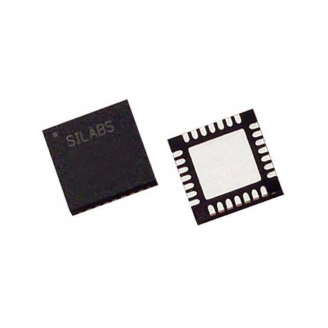
| 产品图片 |
|
| rohs | 符合RoHS无铅 / 符合限制有害物质指令(RoHS)规范要求 |
| 产品系列 | RF集成电路,锁相环 - PLL,Silicon Labs SI4133-D-GM- |
| 数据手册 | |
| 产品型号 | SI4133-D-GMSI4133-D-GM |
| PLL | 是 |
| 产品目录页面 | |
| 产品种类 | 锁相环 - PLL |
| 供应商器件封装 | 28-QFN(5x5) |
| 其它名称 | 336-1113 |
| 分频器/倍频器 | 是/无 |
| 包装 | 托盘 |
| 单位重量 | 63.600 mg |
| 商标 | Silicon Labs |
| 安装类型 | 表面贴装 |
| 安装风格 | SMD/SMT |
| 封装 | Tray |
| 封装/外壳 | 28-VFQFN 裸露焊盘 |
| 封装/箱体 | MLP-28 |
| 工作温度 | -40°C ~ 85°C |
| 工作电源电压 | 2.7 V to 3.6 V |
| 工厂包装数量 | 490 |
| 差分-输入:输出 | 无/无 |
| 最大工作温度 | + 85 C |
| 最大输入频率 | 26 MHz |
| 最小工作温度 | - 40 C |
| 最小输入频率 | 2 MHz |
| 标准包装 | 490 |
| 比率-输入:输出 | 1:3 |
| 电压-电源 | 2.7 V ~ 3.6 V |
| 电源电压-最大 | 3.6 V |
| 电源电压-最小 | 2.7 V |
| 电路数 | 1 |
| 电路数量 | 3 |
| 类型 | RF Synthesizer频率合成器 |
| 系列 | SI4133 |
| 输入 | |
| 输出 | 时钟 |
| 频率-最大值 | 1.8GHz |


- 商务部:美国ITC正式对集成电路等产品启动337调查
- 曝三星4nm工艺存在良率问题 高通将骁龙8 Gen1或转产台积电
- 太阳诱电将投资9.5亿元在常州建新厂生产MLCC 预计2023年完工
- 英特尔发布欧洲新工厂建设计划 深化IDM 2.0 战略
- 台积电先进制程称霸业界 有大客户加持明年业绩稳了
- 达到5530亿美元!SIA预计今年全球半导体销售额将创下新高
- 英特尔拟将自动驾驶子公司Mobileye上市 估值或超500亿美元
- 三星加码芯片和SET,合并消费电子和移动部门,撤换高东真等 CEO
- 三星电子宣布重大人事变动 还合并消费电子和移动部门
- 海关总署:前11个月进口集成电路产品价值2.52万亿元 增长14.8%


PDF Datasheet 数据手册内容提取
Si4133 Si4123/22/13/12 DUAL-BAND RF SYNTHESIZER WITH INTEGRATED VCOS FOR WIRELESS COMMUNICATIONS FEATURES Dual-band RF synthesizers Low phase noise RF1: 900MHz to 1.8GHz Programmable powerdown modes RF2: 750MHz to 1.5GHz 1µA standby current IF synthesizer 18mA typical supply current IF: 62.5to1000 MHz 2.7 to 3.6V operation Integrated VCOs, loop filters, Packages: 24-pin TSSOP, varactors, and resonators 28-lead QFN Ordering Information: Minimal (2) number of external Lead-free and RoHS compliant See page31. components required Applications Pin Assignments Dual-band communications Digital cellular telephones GSM850, E-GSM900, DCS1800, Si4133-GT PCS1900 Digital cordless phones SCLK 1 24 SEN Analog cordless phones SDATA 2 23 VDDI Wireless local loop GNDR 3 22 IFOUT RFLD 4 21 GNDI Description RFLC 5 20 IFLB GNDR 6 19 IFLA The Si4133 is a monolithic integrated circuit that performs both IF and dual- band RF synthesis for wireless communications applications. The Si4133 RFLB 7 18 GNDD includes three VCOs, loop filters, reference and VCO dividers, and phase RFLA 8 17 VDDD detectors. Divider and powerdown settings are programmable with a three- GNDR 9 16 GNDD wire serial interface. GNDR 10 15 XIN RFOUT 11 14 PWDN Functional Block Diagram VDDR 12 13 AUXOUT Si4133-GM XIN RAemfeprleifniecre R Phase RFLA Powerdown Detector RF1 RFLB GNDR SDATA SCLK SEN VDDI IFOUT GNDI PWDN Control N RFOUT 28 27 26 25 24 23 22 GNDR 1 21 GNDI SDATA Serial R Phase RFLC RFLD 2 20 IFLB SCLK Interface Detector RFLD RFLC 3 19 IFLA 22-bit RF2 GND SEN ReDgaistater N GNDR 4 Pad 18 GNDD RFLB 5 17 VDDD Test R Phase RFLA 6 16 GNDD AUXOUT IFDIV IFOUT Mux Detector GNDR 7 15 XIN IF IFLA 8 9 10 11 12 13 14 N IFLB NDR NDR OUT DDR OUT WDN NDD G G RF V UX P G A Patents pending Rev. 1.61 1/10 Copyright © 2010 by Silicon Laboratories Si4133
Si4133 2 Rev. 1.61
Si4133 TABLE OF CONTENTS Section Page 1. Electrical Specifications . . . . . . . . . . . . . . . . . . . . . . . . . . . . . . . . . . . . . . . . . . . . . . . . . . .4 2. Typical Application Circuits . . . . . . . . . . . . . . . . . . . . . . . . . . . . . . . . . . . . . . . . . . . . . . .15 3. Functional Description . . . . . . . . . . . . . . . . . . . . . . . . . . . . . . . . . . . . . . . . . . . . . . . . . . .16 3.1. Serial Interface . . . . . . . . . . . . . . . . . . . . . . . . . . . . . . . . . . . . . . . . . . . . . . . . . . . . .16 3.2. Setting the VCO Center Frequencies . . . . . . . . . . . . . . . . . . . . . . . . . . . . . . . . . . . .16 3.3. Extended Frequency Operation . . . . . . . . . . . . . . . . . . . . . . . . . . . . . . . . . . . . . . . .17 3.4. Self-Tuning Algorithm . . . . . . . . . . . . . . . . . . . . . . . . . . . . . . . . . . . . . . . . . . . . . . . .17 3.5. Output Frequencies . . . . . . . . . . . . . . . . . . . . . . . . . . . . . . . . . . . . . . . . . . . . . . . . . .18 3.6. PLL Loop Dynamics . . . . . . . . . . . . . . . . . . . . . . . . . . . . . . . . . . . . . . . . . . . . . . . . .18 3.7. RF and IF Outputs . . . . . . . . . . . . . . . . . . . . . . . . . . . . . . . . . . . . . . . . . . . . . . . . . . .19 3.8. Reference Frequency Amplifier . . . . . . . . . . . . . . . . . . . . . . . . . . . . . . . . . . . . . . . . .19 3.9. Powerdown Modes . . . . . . . . . . . . . . . . . . . . . . . . . . . . . . . . . . . . . . . . . . . . . . . . . .19 3.10. Auxiliary Output (AUXOUT) . . . . . . . . . . . . . . . . . . . . . . . . . . . . . . . . . . . . . . . . . .20 4. Control Registers . . . . . . . . . . . . . . . . . . . . . . . . . . . . . . . . . . . . . . . . . . . . . . . . . . . . . . . .21 5. Pin Descriptions: Si4133-GT . . . . . . . . . . . . . . . . . . . . . . . . . . . . . . . . . . . . . . . . . . . . . . .27 6. Pin Descriptions: Si4133-GM . . . . . . . . . . . . . . . . . . . . . . . . . . . . . . . . . . . . . . . . . . . . . .29 7. Ordering Guide . . . . . . . . . . . . . . . . . . . . . . . . . . . . . . . . . . . . . . . . . . . . . . . . . . . . . . . . . .31 8. Si4133 Derivative Devices . . . . . . . . . . . . . . . . . . . . . . . . . . . . . . . . . . . . . . . . . . . . . . . . .31 9. Package Outline: Si4133-GT . . . . . . . . . . . . . . . . . . . . . . . . . . . . . . . . . . . . . . . . . . . . . . .32 10. Package Outline: Si4133-GM . . . . . . . . . . . . . . . . . . . . . . . . . . . . . . . . . . . . . . . . . . . . . .33 Document Change List . . . . . . . . . . . . . . . . . . . . . . . . . . . . . . . . . . . . . . . . . . . . . . . . . . . . .34 Contact Information . . . . . . . . . . . . . . . . . . . . . . . . . . . . . . . . . . . . . . . . . . . . . . . . . . . . . . . .36 Rev. 1.61 3
Si4133 1. Electrical Specifications Table 1. Recommended Operating Conditions Parameter Symbol Test Condition Min Typ Max Unit Ambient Temperature T –40 25 85 °C A Supply Voltage V 2.7 3.0 3.6 V DD Supply Voltages Difference V (V – V ), –0.3 — 0.3 V DDR DDD (V – V ) DDI DDD Note: All minimum and maximum specifications are guaranteed and apply across the recommended operating conditions. Typical values apply at nominal supply voltages and an operating temperature of 25°C unless otherwise stated. Table 2. Absolute Maximum Ratings1,2 Parameter Symbol Value Unit DC Supply Voltage V –0.5 to 4.0 V DD Input Current3 IIN ±10 mA Input Voltage3 VIN –0.3 to VDD+0.3 V Storage Temperature Range TSTG –55 to 150 oC Notes: 1. Permanent device damage may occur if the above Absolute Maximum Ratings are exceeded. Functional operation should be restricted to the conditions as specified in the operational sections of this data sheet. Exposure to absolute maximum rating conditions for extended periods may affect device reliability. 2. This device is a high performance RF integrated circuit with an ESD rating of <2kV. Handling and assembly of this device should only be done at ESD-protected workstations. 3. For signals SCLK, SDATA, SEN, PWDN and XIN. 4 Rev. 1.61
Si4133 Table 3. DC Characteristics (V = 2.7 to 3.6V, T = –40 to 85°C) DD A Parameter Symbol Test Condition Min Typ Max Unit Total Supply Current1 RF1 and IF operating — 18 27 mA RF1 Mode Supply Current1 — 10 16 mA RF2 Mode Supply Current1 — 9 16 mA IF Mode Supply Current1 — 8 13 mA Standby Current PWDN = 0 — 1 — µA High Level Input Voltage2 V 0.7 V — — V IH DD Low Level Input Voltage2 V — — 0.3 V V IL DD High Level Input Current2 I V = 3.6 V, –10 — 10 µA IH IH V = 3.6 V DD Low Level Input Current2 I V = 0 V, –10 — 10 µA IL IL V = 3.6 V DD High Level Output Voltage3 V I = –500 µA V –0.4 — — V OH OH DD Low Level Output Voltage3 V I = 500 µA — — 0.4 V OL OH Notes: 1. RF1 = 1.6GHz, RF2 = 1.1GHz, IFOUT = 550MHz, LPWR = 0. 2. For signals SCLK, SDATA, SEN, and PWDN. 3. For signal AUXOUT. Rev. 1.61 5
Si4133 Table 4. Serial Interface Timing (V = 2.7 to 3.6V, T = –40 to 85°C) DD A Parameter1 Symbol Test Condition Min Typ Max Unit SCLK Cycle Time t Figure1 40 — — ns clk SCLK Rise Time t Figure1 — — 50 ns r SCLK Fall Time t Figure1 — — 50 ns f SCLK High Time t Figure1 10 — — ns h SCLK Low Time t Figure1 10 — — ns l SDATA Setup Time to SCLK2 t Figure2 5 — — ns su SDATA Hold Time from SCLK2 t Figure2 0 — — ns hold SEN to SCLKDelay Time2 t Figure2 10 — — ns en1 SCLK to SENDelay Time2 t Figure2 12 — — ns en2 SEN to SCLKDelay Time2 t Figure2 12 — — ns en3 SEN Pulse Width t Figure2 10 — — ns w Notes: 1. All timing is referenced to the 50% level of the waveforms unless otherwise noted. 2. Timing is not referenced to 50% level of the waveform. See Figure2. t t r f 80% SCLK 50% 20% t t h l t clk Figure 1. SCLK Timing Diagram 6 Rev. 1.61
Si4133 t t su hold SCLK SDATA D17 D16 D15 A1 A0 t t en3 en1 t en2 SENB t w Figure 2. Serial Interface Timing Diagram First bit Last bit clocked in clocked in D D D D D D D D D D D D D D D D D D A A A A 17 16 15 14 13 12 11 10 9 8 7 6 5 4 3 2 1 0 3 2 1 0 data address field field Figure 3. Serial Word Format Rev. 1.61 7
Si4133 Table 5. RF and IF Synthesizer Characteristics (V = 2.7 to 3.6V, T = –40 to 85°C) DD A Parameter1 Symbol Test Condition Min Typ Max Unit XIN Input Frequency f 2 — 26 MHz REF Reference Amplifier Sensitivity V 0.5 — V V REF DD PP +0.3 V Phase Detector Update Frequency f f = f /R 0.010 — 1.0 MHz REF RF1 VCO Center Frequency Range f 947 — 1720 MHz CEN RF1 VCO Tuning Range2 Extended frequency 1850 — 2050 MHz operation RF2 VCO Center Frequency Range f 789 — 1429 MHz CEN RF Tuning Range from f Note: L ±10% –5 — 5 % CEN EXT IF VCO Center Frequency Range f 526 — 952 MHz CEN IFOUT Tuning Range with IFDIV 62.5 — 1000 MHz IFOUT Tuning Range from f Note: L ±10% –5 — 5 % CEN EXT RF1 VCO Pushing Open loop — 500 — kHz/V RF2 VCO Pushing — 400 — kHz/V IF VCO Pushing — 300 — kHz/V RF1 VCO Pulling VSWR = 2:1, all — 400 — kHz PP phases, open loop RF2 VCO Pulling — 300 — kHz PP IF VCO Pulling — 100 — kHz PP RF1 Phase Noise 1 MHz offset — –132 — dBc/Hz RF1 Integrated Phase Error 10Hz to 100kHz — 0.9 — degrees rms RF2 Phase Noise 1MHz offset — –134 — dBc/Hz RF2 Integrated Phase Error 10Hz to 100kHz — 0.7 — degrees rms IF Phase Noise 100kHz offset — –117 — dBc/Hz IF Integrated Phase Error 100Hz to 100kHz — 0.4 — degrees rms Notes: 1. f = 200 kHz, RF1 = 1.6GHz, RF2 = 1.2GHz, IFOUT = 550MHz, LPWR = 0, for all parameters unless otherwise noted. 2. Extended frequency operation only. V 3.0V, QFN only, VCO Tuning Range fixed by directly shorting the RFLA and DD RFLB pins. See Application Note 41 for more details on the Si4133 extended frequency operation. 3. From powerup request (PWDN or SEN during a write of 1 to bits PDIB and PDRB in Register2) to RF and IF synthesizers ready (settled to within 0.1ppm frequency error). 4. From powerdown request (PWDN, or SENduring a write of 0 to bits PDIB and PDRB in Register2) to supply current equal to I . PWDN 8 Rev. 1.61
Si4133 Table 5. RF and IF Synthesizer Characteristics (Continued) (V = 2.7 to 3.6V, T = –40 to 85°C) DD A Parameter1 Symbol Test Condition Min Typ Max Unit RF1 Harmonic Suppression Second Harmonic — –26 –20 dBc RF2 Harmonic Suppression — –26 –20 dBc IF Harmonic Suppression — –26 –20 dBc RFOUT Power Level Z = 50 –8 –3 1 dBm L RFOUT Power Level2 Z = 50RF1 active, –14 –7 1 dBm L Extended frequency operation IFOUT Power Level Z = 50 –8 –4 0 dBm L RF1 Output Reference Spurs Offset = 200 kHz — –65 — dBc Offset = 400 kHz — –71 — dBc Offset = 600 kHz — –75 — dBc RF2 Output Reference Spurs Offset = 200 kHz — –65 — dBc Offset = 400 kHz — –71 — dBc Offset = 600 kHz — –75 — dBc Powerup Request to Synthesizer Ready3 t Figures 4, 5 — 40/f 50/f pup Time Powerdown Request to Synthesizer Off4 t Figures 4, 5 — — 100 ns pdn Time Notes: 1. f = 200 kHz, RF1 = 1.6GHz, RF2 = 1.2GHz, IFOUT = 550MHz, LPWR = 0, for all parameters unless otherwise noted. 2. Extended frequency operation only. V 3.0V, QFN only, VCO Tuning Range fixed by directly shorting the RFLA and DD RFLB pins. See Application Note 41 for more details on the Si4133 extended frequency operation. 3. From powerup request (PWDN or SEN during a write of 1 to bits PDIB and PDRB in Register2) to RF and IF synthesizers ready (settled to within 0.1ppm frequency error). 4. From powerdown request (PWDN, or SENduring a write of 0 to bits PDIB and PDRB in Register2) to supply current equal to I . PWDN Rev. 1.61 9
Si4133 RF and IF synthesizers settled to within 0.1 ppm frequency error. t t pup pdn I T I PWDN SEN SDATA PDIB = 1 PDIB = 0 PDRB = 1 PDRB = 0 Figure 4. Software Power Management Timing Diagram RF and IF synthesizers settled to within 0.1 ppm frequency error. t t pup pdn I T I PWDN PWDN Figure 5. Hardware Power Management Timing Diagram 10 Rev. 1.61
Si4133 TRACE A: Ch1 FM Main Time A Marker 174.04471 us 711.00 Hz 1.424 kHz Real 160 Hz /div 176 Hz Start: 0 s Stop: 399.6003996 us Figure 6. Typical Transient Response RF1 at 1.6 GHz with 200 kHz Phase Detector Update Frequency Rev. 1.61 11
Si4133 −60 −70 −80 z) −90 H c/ B d se (−100 oi N e s a Ph−110 −120 −130 −140 102 103 104 105 106 Offset Frequency (Hz) Figure 7. Typical RF1 Phase Noise at 1.6 GHz with 200 kHz Phase Detector Update Frequency Figure 8. Typical RF1 Spurious Response at 1.6 GHz with 200 kHz Phase Detector Update Frequency 12 Rev. 1.61
Si4133 −60 −70 −80 z) −90 H c/ B d se (−100 oi N e s a Ph−110 −120 −130 −140 102 103 104 105 106 Offset Frequency (Hz) Figure 9. Typical RF2 Phase Noise at 1.2 GHz with 200 kHz Phase Detector Update Frequency Figure 10. Typical RF2 Spurious Response at 1.2 GHz with 200 kHz Phase Detector Update Frequency Rev. 1.61 13
Si4133 −70 −80 −90 z)−100 H c/ B d se (−110 oi N e s a Ph−120 −130 −140 −150 102 103 104 105 106 Offset Frequency (Hz) Figure 11. Typical IF Phase Noise at 550 MHz with 200 kHz Phase Detector Update Frequency Figure 12. IF Spurious Response at 550 MHz with 200 kHz Phase Detector Update Frequency 14 Rev. 1.61
Si4133 2. Typical Application Circuits V DD Si4133-GT From 30 * 1 24 System SCLK SEN 0.022F Controller 2 23 SDATA VDDI 40 nH 560 pF 3 22 GNDR IFOUT IFOUT 4 21 RFLD GNDI Printed Trace 5 20 RFLC IFLB Inductor or Chip Inductor Printed Trace 6 19 GNDR IFLA Inductors 7 18 RFLB GNDD V 0.022F 8 17 DD RFLA VDDD 9 16 GNDR GNDD 560 pF 10 15 GNDR XIN External Clock 560 pF 2 nH 11 14 RFOUT RFOUT PWDN PWDN 0.022F VDD 12 13 VDDR AUXOUT AUXOUT * Add 30 series resistance if using IF output divide values 2, 4, or 8. Figure 13. Si4133-GT V DD 30 * From 0.022F System 40 nH 560 pF Controller IFOUT 28 27 26 25 24 23 22 1 GNDR SDATA SCLK SEN VDDI IFOUT GNDI 21 Printed Trace GNDR GNDI Inductor or 2 20 Chip Inductor RFLD IFLB 3 19 RFLC IFLA Printed Trace 4 18 GNDR Si4133-GM GNDD V Inductors DD 5 17 RFLB VDDD 6 16 0.022F RFLA GNDD 560 pF 7 GNDRR R UT R OUT N D XIN 15 External Clock D D O D X D D N N F D U W N G G R V A P G 8 9 10 11 12 13 14 V DD 0.022F AUXOUT PWDN 2 nH 560 pF RFOUT * Add 30 series resistance if using IF output divide values 2, 4, or 8. Figure 14. Si4133-GM Rev. 1.61 15
Si4133 3. Functional Description The unique PLL architecture used in the Si4133 produces settling (lock) times that are comparable in The Si4133 is a monolithic integrated circuit that speed to fractional-N architectures without the high performs IF and dual-band RF synthesis for wireless phase noise or spurious modulation effects often communications applications. This integrated circuit associated with those designs. (IC), with minimal external components, completes the 3.1. Serial Interface frequency synthesis function necessary for RF communications systems. A timing diagram for the serial interface is shown in The Si4133 has three complete phase-locked loops Figure2 on page 7. Figure3 on page 7 shows the (PLLs) with integrated voltage-controlled oscillators format of the serial word. (VCOs). The low phase noise of the VCOs makes the The Si4133 is programmed serially with 22-bit words Si4133 suitable for demanding wireless comprised of 18-bit data fields and 4-bit address fields. communications applications. Phase detectors, loop When the serial interface is enabled (i.e., when SEN is filters, and reference and output frequency dividers are low) data and address bits on the SDATA pin are integrated. The IC is programmed with a three-wire clocked into an internal shift register on the rising edge serial interface. of SCLK. Data in the shift register is then transferred on Two PLLs are provided for dual-band RF synthesis. the rising edge of SEN into the internal data register These RF PLLs are multiplexed so that only one PLL is addressed in the address field. The serial interface is active at a time, as determined by the setting of an disabled when SEN is high. internal register. The active PLL is the last one to be Table12 on page21 summarizes the data register written. The center frequency of the VCO in each PLL is functions and addresses. The internal shift register set by the value of an external inductance. Inaccuracies ignores leading bits before the 22 required bits. in these inductances are compensated for by the self- 3.2. Setting the VCO Center Frequencies tuning algorithm. The algorithm is run after powerup or after a change in the programmed output frequency. The PLLs can adjust the IF and RF output frequencies Each RF PLL, when active, can adjust the RF output ±5% of the center frequencies of their VCOs. Each frequency by ±5% of its VCO’s center frequency. center frequency is established by the value of an Because the two VCOs can be set to have widely external inductance connected to the respective VCO. separated center frequencies, the RF output can be Manufacturing tolerances of ±10% for the external programmed to service two widely separated frequency inductances are acceptable. The Si4133 compensates bands by programming the corresponding N-Divider. for inaccuracies in each inductance by executing a self- One RF VCO is optimized to have its center frequency tuning algorithm after PLL powerup or after a change in set between 947MHz and 1.72GHz, while the second the programmed output frequency. RF VCO is optimized to have its center frequency set Because the total tank inductance is in the low nH between 789MHz and 1.429GHz. range, the inductance of the package must be One PLL is provided for IF frequency synthesis. The considered when determining the correct external center frequency of this circuit’s VCO is set by the inductance. The total inductance (LTOT) presented to connection of an external inductance. The PLL can each VCO is the sum of the external inductance (LEXT) adjust the IF output frequency by ±5% of the VCO and the package inductance (LPKG). Each VCO has a center frequency. Inaccuracies in the value of the nominal capacitance (CNOM) in parallel with the total external inductance are compensated for by the inductance, and the center frequency is as follows: Si4133’s proprietary self-tuning algorithm. This 1 algorithm is initiated each time the PLL is powered-up f = ----------------------------------------------- CEN (by either the PWDN pin or by software) and/or each 2 LTOTCNOM time a new output frequency is programmed. or The IF VCO can have its center frequency set as low as 526MHz and as high as 952MHz. An IF output divider 1 f = ------------------------------------------------------------------------ divides down the IF output frequencies, if needed. The CEN 2 L +L C PKG EXT NOM divider is programmable and is capable of dividing by 1, 2, 4, or 8. Tables 6 and 7 summarize the characteristics of each VCO. 16 Rev. 1.61
Si4133 the correct total inductance to the VCO. In Table 6. Si4133-GT VCO Characteristics manufacturing, the external inductance can vary ±10% of its nominal value and the Si4133 corrects for the VCO f Range C L L Range CEN NOM PKG EXT variation with the self-tuning algorithm. (MHz) (pF) (nH) (nH) For more information on designing the external trace Min Max Min Max inductors, refer to Application Note 31: Inductor Design for the Si41xx Synthesizer Family. RF1 947 1720 4.3 2.0 0.0 4.6 3.3. Extended Frequency Operation RF2 789 1429 4.8 2.3 0.3 6.2 The Si4133 may operate at an extended frequency range of 1850MHz to 2050MHz by connecting the IF 526 952 6.5 2.1 2.2 12.0 RFLA and RFLB pins directly. For information on configuring the Si4133 for extended frequency Table 7. Si4133-GM VCO Characteristics operation, refer to Application Note 41: Extended Frequency Operation of Silicon Laboratories Frequency VCO f Range C L L Range Synthesizers. CEN NOM PKG EXT (MHz) (pF) (nH) (nH) 3.4. Self-Tuning Algorithm Min Max Min Max The self-tuning algorithm is initiated immediately after powerup of a PLL or, if the PLL is already powered, after RF1 947 1720 4.3 1.5 0.5 5.1 a change in its programmed output frequency. This algorithm attempts to tune the VCO so that its free- RF2 789 1429 4.8 1.5 1.1 7.0 running frequency is near the required output frequency. In doing so, the algorithm compensates for IF 526 952 6.5 1.6 2.7 12.5 manufacturing tolerance errors in the value of the external inductance connected to the VCO. It also reduces the frequency error for which the PLL must correct to get the precise required output frequency. The self-tuning algorithm leaves the VCO oscillating at a frequency in error by somewhat less than 1% of the L desired output frequency. PKG 2 After self-tuning, the PLL controls the VCO oscillation L frequency. The PLL completes frequency locking, EXT eliminating any remaining frequency error. From then on, it maintains frequency-lock, compensating for effects of temperature and supply voltage variations. L PKG The Si4133’s self-tuning algorithm compensates for 2 component value errors at any temperature within the specified temperature range. However, the ability of the Figure 15. External Inductance Connection PLL to compensate for drift in component values that As a design example, consider that the goal is to occur after self-tuning is limited. For external synthesize frequencies in a 25MHz band between inductances with temperature coefficients 1120and1145MHz using the Si4133-GT. The center approximately ±150ppm/oC, the PLL can maintain lock frequency should be defined as midway between the for changes in temperature of approximately ±30oC. two extremes, or 1132.5MHz. The PLL can adjust the Applications where the PLL is regularly powered down VCO output frequency ±5% of the center frequency, or or the frequency is periodically reprogrammed minimize ±56.6MHz of 1132.5MHz (i.e., from approximately or eliminate the potential effects of temperature drift 1076to1189MHz). The RF2 VCO has a CNOM of because the VCO is re-tuned in either case. In 4.8pF. A 4.1nH inductance in parallel with this applications where the ambient temperature can drift capacitance yields the required center frequency. An substantially after self-tuning, it might be necessary to external inductance of 1.8nH should be connected monitor the lock-detect bar (LDETB) signal on the between RFLC and RFLD as shown in Figure15. This, AUXOUT pin to determine whether a PLL is about to in addition to 2.3nH of package inductance, presents run out of locking capability. See “3.10. Auxiliary Output Rev. 1.61 17
Si4133 (AUXOUT)” for how to select LDETB. The LDETB setting the bits to 11. The values of the available gains, signal is low after self-tuning is completed but rises relative to the highest gain, are as follows: when the IF or RF PLL nears the limit of its compensation range. LDETB is also high when either Table 8. Gain Values (Register 1) PLL is executing the self-tuning algorithm. The output Relative P.D. frequency is still locked when LDETB goes high, but the K Bits P Gain PLL eventually loses lock if the temperature continues to drift in the same direction. Therefore, if LDETB goes 00 1 high both the IF and RF PLLs should be re-tuned 01 1/2 promptly by initiating the self-tuning algorithm. 10 1/4 3.5. Output Frequencies 11 1/8 The IF and RF output frequencies are set by The gain value bits is automatically set with the Auto K programming the R- and N-Divider registers. Each PLL P bit (bit 2) in the Main Configuration register to 1. In has R and N registers so that each can be programmed setting this bit, the gain values are optimized for a given independently. Programming either the R- or N-Divider value of N. In general, a higher phase detector gain register for RF1 or RF2 automatically selects the decreases in-band phase noise and increase the speed associated output. of the PLL transient until the point at which stability The reference frequency on the XIN pin is divided by R begins to be compromised. The optimal gain depends and this signal is input to the PLL’s phase detector. The on N. Table9 lists recommended settings for different other input to the phase detector is the PLL’s VCO values of N. These are the settings when the Auto K bit P output frequency divided by N. The PLL acts to make is set. these frequencies equal. That is, after an initial transient: Table 9. Optimal KP Settings RF1 RF2 IF f f N --O----U----T-- = --R----E----F- KP1<1:0> KP2<3:2> KPI<5:4> N R 2047 00 00 00 or 2048 to 4095 00 00 01 N fOUT = R----fREF 4096 to 8191 00 01 10 The R values are set by programming the RF1 R- 8192 to 16383 01 10 11 Divider register (Register6), the RF2R-Divider register 16384 to 32767 10 11 11 (Register7) and the IF R-Divider register (Register8). 32768 11 11 11 The N values are set by programming the RF1 N- Divider register (Register3), the RF2 N-Divider register The VCO gain and loop filter characteristics are not (Register4), and the IF N-Divider register (Register5). programmable. Each N-Divider is implemented as a conventional high The settling time for the PLL is directly proportional to its speed divider. That is, it consists of a dual-modulus phase detector update period T (T equals 1/f ). A prescaler, a swallow counter, and a lower speed typical transient response is shown in Figure6 on page synchronous counter. However, the control of these 11. During the first 13 update periods the Si4133 sub-circuits is automatically handled. Only the executes the self-tuning algorithm. From then on the appropriate Nvalue should be programmed. PLL controls the output frequency. Because of the 3.6. PLL Loop Dynamics unique architecture of the Si4133 PLLs, the time required to settle the output frequency to 0.1ppm error The transient response for each PLL is determined by is automatically 25 update periods. The total time after its phase detector update rate f (equal to f /R) and REF powerup or a change in programmed frequency until the the phase detector gain programmed for each RF1, synthesized frequency is settled—including time for RF2, or IF synthesizer. See Register1. Four different self-tuning—is approximately 40 update periods. settings for the phase detector gain are available for each PLL. The highest gain is programmed by setting Note: The settling time analysis holds for RF1 f 500kHz. the two phase detector gain bits to 00, and the lowest by For RF1 f > 500kHz, the settling time is larger. 18 Rev. 1.61
Si4133 3.7. RF and IF Outputs For frequencies less than 500MHz, the IF output buffer can directly drive a 200 resistive load or higher. For The RFOUT and IFOUT pins are driven by amplifiers resistive loads greater than 500 (f < 500MHz) the that buffer the RF VCOs and IF VCO respectively. The LPWR bit can be set to reduce the power consumed by RF output amplifier receives its input from the RF1 or the IF output buffer. See Figure17. RF2 VCO, depending on which R- or N-Divider register is written last. For example, programming the N-Divider >500 pF register for RF1 automatically selects the RF1 VCO IFOUT output. Figures 13 and 14 show application diagrams for the Si4133. The RF output signal must be ac coupled to its >200 load through a capacitor. An external inductance between the RFOUT pin and the ac coupling capacitor is required as part of an output matching network to maximize power delivered to the load. This 2nH Figure 17. IF Frequencies < 500 MHz inductance can be realized with a PC board trace. The 3.8. Reference Frequency Amplifier network is made to provide an adequate match to an external 50 load for both the RF1 and RF2 frequency The Si4133 provides a reference frequency amplifier. If bands. The matching network also filters the output the driving signal has CMOS levels it can be connected signal to reduce harmonic distortion. directly to the XIN pin. Otherwise, the reference frequency signal should be ac coupled to the XIN pin The IFOUT pin must also be ac coupled to its load through a 560pF capacitor. through a capacitor. The IF output level is dependent upon the load. Figure18 on page 20 displays the output 3.9. Powerdown Modes level versus load resistance for a variety of output Table11 summarizes the powerdown functionality. The frequencies. For resistive loads greater than 500 the Si4133 can be powered down by taking the PWDN pin low output level saturates and the bias currents in the IF or by setting bits in the Powerdown register (Register2). output amplifier are higher than required. The LPWR bit When the PWDN pin is low, the Si4133 is powered down in the Main Configuration register (Register0) can be regardless of the Powerdown register settings. When the set to 1 to reduce the bias currents and therefore reduce PWDN pin is high, power management is in control of the the power dissipated by the IF amplifier. For loads less Powerdown register bits. than 500 LPWR should be set to 0 to maximize the output level. The IF and RF sections of the Si4133 circuitry can be individually powered down by setting the Powerdown For IF frequencies greater than 500MHz, a matching register bits PDIB and PDRB low, respectively. The network is required to drive a 50load. See Figure16. reference frequency amplifier is also powered up if the The value of L can be determined from Table10. MATCH PDRB and PDIB bits are high. Also, setting the AUTOPDB Table 10. L Values bit to 1 in the Main Configuration register (Register0) is MATCH equivalent to setting both bits in the Powerdown register to Frequency L 1. MATCH The serial interface remains available and can be written in 500–600MHz 40nH all powerdown modes. 600–800MHz 27nH 800MHz–1GHz 18nH 560 pF IFOUT L MATCH 50 Figure 16. IF Frequencies > 500 MHz Rev. 1.61 19
Si4133 3.10. Auxiliary Output (AUXOUT) The signal appearing on AUXOUT is selected by setting the AUXSEL bits in the Main Configuration register (Register0). The LDETB signal can be selected by setting the AUXSEL bits to 11. This signal can be used to indicate that the IF or RF PLL is going to lose lock because of excessive ambient temperature drift and should be re-tuned. The LDETB signal indicates a logical OR result if both IF and RF are simultaneously generating a signal. Table 11. Powerdown Configuration PWDN Pin AUTOPDB PDIB PDRB IF Circuitry RF Circuitry PWDN = 0 X X X OFF OFF 0 0 0 OFF OFF 0 0 1 OFF ON PWDN = 1 0 1 0 ON OFF 0 1 1 ON ON 1 x x ON ON 450 400 350 LPWR=1 LPWR=0 300 ms) Vr m250 ge ( olta ut V200 p ut O 150 100 50 0 0 200 400 600 800 1000 1200 Load Resistance () Figure 18. Typical IF Output Voltage vs. Load Resistance at 550 MHz 20 Rev. 1.61
Si4133 4. Control Registers Table 12. Register Summary Register Name Bit Bit Bit Bit Bit Bit Bit Bit Bit Bit Bit Bit Bit Bit Bit Bit Bit Bit 17 16 15 14 13 12 11 10 9 8 7 6 5 4 3 2 1 0 0 Main 0 0 0 0 AUXSEL IFDIV 0 0 0 0 LPWR 0 AUTO AUTO RF 0 Configura- [1:0] [1:0] PDB KP PWR tion 1 Phase 0 0 0 0 0 0 0 0 0 0 0 0 K [1:0] K [1:0] K [1:0] PI P2 P1 Detector Gain 2 Powerdown 0 0 0 0 0 0 0 0 0 0 0 0 0 0 0 0 PDIB PDRB 3 RF1 N [17:0] RF1 N-Divider 4 RF2 0 N [16:0] RF2 N-Divider 5 IF N-Divider 0 0 N [15:0] IF 6 RF1 0 0 0 0 0 R [12:0] RF1 R-Divider 7 RF2 0 0 0 0 0 R [12:0] RF2 R-Divider 8 IF R-Divider 0 0 0 0 0 R [12:0] IF 9 Reserved . . . 15 Reserved Note: Registers 9–15 are reserved. Writes to these registers might result in unpredictable behavior. Registers not listed here are reserved and should not be written. Rev. 1.61 21
Si4133 Register 0. Main Configuration Address Field = A[3:0] = 0000 Bit D17 D16 D15 D14 D13 D12 D11 D10 D9 D8 D7 D6 D5 D4 D3 D2 D1 D0 Name 0 0 0 0 AUXSEL IFDIV 0 0 0 0 LPWR 0 AUTO AUTO RF 0 [1:0] [1:0] PDB KP PWR Bit Name Function 17:14 Reserved Program to zero. 13:12 AUXSEL[1:0] Auxiliary Output Pin Definition. 00 = Reserved. 01 = Force output low. 10 = Reserved. 11 = Lock Detect—LDETB. 11:10 IFDIV[1:0] IF Output Divider. 00 = IFOUT = IFVCO Frequency 01 = IFOUT = IFVCO Frequency/2 10 = IFOUT = IFVCO Frequency/4 11 = IFOUT = IFVCO Frequency/8 9:6 Reserved Program to zero. 5 LPWR Output Power-Level Settings for IF Synthesizer Circuit. 0 = R 500—normal power mode. LOAD 1 = R 500—low power mode. LOAD 4 Reserved Program to zero. 3 AUTOPDB Auto Powerdown. 0 = Software powerdown is controlled by Register2. 1 = Equivalent to setting all bits in Register2 = 1. 2 AUTOK Auto K Setting. P P 0 = K s are controlled by Register1. P 1 = K s are set according to Table9 on page18. P 1 RFPWR Program to zero. (Used for extended frequency operation. See AN41 for more information.) 0 Reserved Program to zero. 22 Rev. 1.61
Si4133 Register 1. Phase Detector Gain Address Field (A[3:0]) = 0001 Bit D17 D16 D15 D14 D13 D12 D11 D10 D9 D8 D7 D6 D5 D4 D3 D2 D1 D0 Name 0 0 0 0 0 0 0 0 0 0 0 0 K [1:0] K [1:0] K [1:0] PI P2 P1 Bit Name Function 17:6 Reserved Program to zero. 5:4 K [1:0] IF Phase Detector Gain Constant.* PI N Value K PI <2048 = 00 2048–4095 = 01 4096–8191 = 10 >8191 = 11 3:2 K [1:0] RF2 Phase Detector Gain Constant.* P2 N Value K P2 <4096 = 00 4096–8191 = 01 8192–16383 = 10 >16383 = 11 1:0 K [1:0] RF1 Phase Detector Gain Constant.* P1 N Value K P1 <8192 = 00 8192–16383 = 01 16384–32767 = 10 >32767 = 11 *Note: When AUTOK = 1, these bits do not need to be programmed. When AUTOK = 0, use these recommended values P P for programming Phase Detector Gain. Rev. 1.61 23
Si4133 Register 2. Powerdown Address Field (A[3:0]) = 0010 Bit D17 D16 D15 D14 D13 D12 D11 D10 D9 D8 D7 D6 D5 D4 D3 D2 D1 D0 Name 0 0 0 0 0 0 0 0 0 0 0 0 0 0 0 0 PDIB PDRB Bit Name Function 17:2 Reserved Program to zero. 1 PDIB Powerdown IF Synthesizer. 0 = IF synthesizer powered down. 1 = IF synthesizer on. 0 PDRB Powerdown RF Synthesizer. 0 = RF synthesizer powered down. 1 = RF synthesizer on. Note: Enabling any PLL with PDIB or PDRB automatically powers on the reference amplifier. Register 3. RF1 N-Divider Address Field (A[3:0]) = 0011 Bit D17 D16 D15 D14 D13 D12 D11 D10 D9 D8 D7 D6 D5 D4 D3 D2 D1 D0 Name N [17:0] RF1 Bit Name Function 17:0 N [17:0] N-Divider for RF1 Synthesizer. RF1 Register 4. RF2 N-Divider Address Field = A[3:0] = 0100 Bit D17 D16 D15 D14 D13 D12 D11 D10 D9 D8 D7 D6 D5 D4 D3 D2 D1 D0 Name 0 N [16:0] RF2 Bit Name Function 17 Reserved Program to zero. 16:0 N [16:0] N-Divider for RF2 Synthesizer. RF2 24 Rev. 1.61
Si4133 Register 5. IF N-Divider Address Field (A[3:0]) = 0101 Bit D17 D16 D15 D14 D13 D12 D11 D10 D9 D8 D7 D6 D5 D4 D3 D2 D1 D0 Name 0 0 N [15:0] IF Bit Name Function 17:16 Reserved Program to zero. 15:0 N [15:0] N-Divider for IF Synthesizer. IF Register 6. RF1 R-Divider Address Field (A[3:0]) = 0110 Bit D17 D16 D15 D14 D13 D12 D11 D10 D9 D8 D7 D6 D5 D4 D3 D2 D1 D0 Name 0 0 0 0 0 R [12:0] RF1 Name Function 17:13 Reserved Program to zero. 12:0 R [12:0] R-Divider for RF1 Synthesizer. RF1 R can be any value from 7 to 8189 if K = 00 RF1 P1 8 to 8189 if K = 01 P1 10 to 8189 if K = 10 P1 14 to 8189 if K = 11 P1 Register 7. RF2 R-Divider Address Field (A[3:0]) = 0111 Bit D17 D16 D15 D14 D13 D12 D11 D10 D9 D8 D7 D6 D5 D4 D3 D2 D1 D0 Name 0 0 0 0 0 R [12:0] RF2 Bit Name Function 17:13 Reserved Program to zero. 12:0 R [12:0] R-Divider for RF2 Synthesizer. RF2 R can be any value from 7 to 8189 if K = 00 RF2 P2 8 to 8189 if K = 01 P2 10 to 8189 if K = 10 P2 14 to 8189 if K = 11 P2 Rev. 1.61 25
Si4133 Register 8. IF R-Divider Address Field (A[3:0]) = 1000 Bit D17 D16 D15 D14 D13 D12 D11 D10 D9 D8 D7 D6 D5 D4 D3 D2 D1 D0 Name 0 0 0 0 0 R [12:0] IF Bit Name Function 17:13 Reserved Program to zero. 12:0 R [12:0] R-Divider for IF Synthesizer. IF R can be any value from 7 to 8189 if K = 00 IF P1 8 to 8189 if K = 01 P1 10 to 8189 if K = 10 P1 14 to 8189 if K = 11 P1 26 Rev. 1.61
Si4133 5. Pin Descriptions: Si4133-GT SCLK 1 24 SEN SDATA 2 23 VDDI GNDR 3 22 IFOUT RFLD 4 21 GNDI RFLC 5 20 IFLB GNDR 6 19 IFLA RFLB 7 18 GNDD RFLA 8 17 VDDD GNDR 9 16 GNDD GNDR 10 15 XIN RFOUT 11 14 PWDN VDDR 12 13 AUXOUT Pin Number Name Description 1 SCLK Serial clock input 2 SDATA Serial data input 3 GNDR Common ground for RF analog circuitry 4 RFLD Pins for inductor connection to RF2 VCO 5 RFLC Pins for inductor connection to RF2 VCO 6 GNDR Common ground for RF analog circuitry 7 RFLB Pins for inductor connection to RF1 VCO 8 RFLA Pins for inductor connection to RF1 VCO 9 GNDR Common ground for RF analog circuitry 10 GNDR Common ground for RF analog circuitry 11 RFOUT Radio frequency (RF) output of the selected RF VCO 12 VDDR Supply voltage for the RF analog circuitry 13 AUXOUT Auxiliary output 14 PWDN Powerdown input pin 15 XIN Reference frequency amplifier input 16 GNDD Common ground for digital circuitry 17 VDDD Supply voltage for digital circuitry 18 GNDD Common ground for digital circuitry 19 IFLA Pins for inductor connection to IF VCO 20 IFLB Pins for inductor connection to IF VCO 21 GNDI Common ground for IF analog circuitry 22 IFOUT Intermediate frequency (IF) output of the IF VCO 23 VDDI Supply voltage for IF analog circuitry 24 SEN Enable serial port input Rev. 1.61 27
Si4133 Table 13. Pin Descriptions for Si4133 Derivatives—TSSOP Pin Number Si4133 Si4123 Si4122 Si4113 Si4112 1 SCLK SCLK SCLK SCLK SCLK 2 SDATA SDATA SDATA SDATA SDATA 3 GNDR GNDR GNDR GNDR GNDD 4 RFLD GNDR RFLD RFLD GNDD 5 RFLC GNDR RFLC RFLC GNDD 6 GNDR GNDR GNDR GNDR GNDD 7 RFLB RFLB GNDR RFLB GNDD 8 RFLA RFLA GNDR RFLA GNDD 9 GNDR GNDR GNDR GNDR GNDD 10 GNDR GNDR GNDR GNDR GNDD 11 RFOUT RFOUT RFOUT RFOUT GNDD 12 VDDR VDDR VDDR VDDR VDDD 13 AUXOUT AUXOUT AUXOUT AUXOUT AUXOUT 14 PWDN PWDN PWDN PWDN PWDN 15 XIN XIN XIN XIN XIN 16 GNDD GNDD GNDD GNDD GNDD 17 VDDD VDDD VDDD VDDD VDDD 18 GNDD GNDD GNDD GNDD GNDD 19 IFLA IFLA IFLA GNDD IFLA 20 IFLB IFLB IFLB GNDD IFLB 21 GNDI GNDI GNDI GNDD GNDI 22 IFOUT IFOUT IFOUT GNDD IFOUT 23 VDDI VDDI VDDI VDDD VDDI 24 SEN SEN SEN SEN SEN 28 Rev. 1.61
Si4133 6. Pin Descriptions: Si4133-GM GNDR SDATA SCLK SEN VDDI IFOUT GNDI 28 27 26 25 24 23 22 GNDR 1 21 GNDI RFLD 2 20 IFLB RFLC 3 19 IFLA GND GNDR 4 18 GNDD Pad RFLB 5 17 VDDD RFLA 6 16 GNDD GNDR 7 15 XIN 8 9 10 11 12 13 14 NDR NDR OUT DDR OUT WDN NDD G G RF V UX P G A Pin Number Name Description 1 GNDR Common ground for RF analog circuitry 2 RFLD Pins for inductor connection to RF2 VCO 3 RFLC Pins for inductor connection to RF2 VCO 4 GNDR Common ground for RF analog circuitry 5 RFLB Pins for inductor connection to RF1 VCO 6 RFLA Pins for inductor connection to RF1 VCO 7 GNDR Common ground for RF analog circuitry 8 GNDR Common ground for RF analog circuitry 9 GNDR Common ground for RF analog circuitry 10 RFOUT Radio frequency (RF) output of the selected RF VCO 11 VDDR Supply voltage for the RF analog circuitry 12 AUXOUT Auxiliary output 13 PWDN Powerdown input pin 14 GNDD Common ground for digital circuitry 15 XIN Reference frequency amplifier input 16 GNDD Common ground for digital circuitry 17 VDDD Supply voltage for digital circuitry 18 GNDD Common ground for digital circuitry 19 IFLA Pins for inductor connection to IF VCO 20 IFLB Pins for inductor connection to IF VCO 21 GNDI Common ground for IF analog circuitry 22 GNDI Common ground for IF analog circuitry 23 IFOUT Intermediate frequency (IF) output of the IF VCO 24 VDDI Supply voltage for IF analog circuitry 25 SEN Enable serial port input 26 SCLK Serial clock input 27 SDATA Serial data input 28 GNDR Common ground for RF analog circuitry Rev. 1.61 29
Si4133 Table 14. Pin Descriptions for Si4133 Derivatives—QFN Pin Number Si4133 Si4123 Si4122 Si4113 Si4112 1 GNDR GNDR GNDR GNDR GNDD 2 RFLD GNDR RFLD RFLD GNDD 3 RFLC GNDR RFLC RFLC GNDD 4 GNDR GNDR GNDR GNDR GNDD 5 RFLB RFLB GNDR RFLB GNDD 6 RFLA RFLA GNDR RFLA GNDD 7 GNDR GNDR GNDR GNDR GNDD 8 GNDR GNDR GNDR GNDR GNDD 9 GNDR GNDR GNDR GNDR GNDD 10 RFOUT RFOUT RFOUT RFOUT GNDD 11 VDDR VDDR VDDR VDDR VDDD 12 AUXOUT AUXOUT AUXOUT AUXOUT AUXOUT 13 PWDN PWDN PWDN PWDN PWDN 14 GNDD GNDD GNDD GNDD GNDD 15 XIN XIN XIN XIN XIN 16 GNDD GNDD GNDD GNDD GNDD 17 VDDD VDDD VDDD VDDD VDDD 18 GNDD GNDD GNDD GNDD GNDD 19 IFLA IFLA IFLA GNDD IFLA 20 IFLB IFLB IFLB GNDD IFLB 21 GNDI GNDI GNDI GNDD GNDI 22 GNDI GNDI GNDI GNDD GNDI 23 IFOUT IFOUT IFOUT GNDD IFOUT 24 VDDI VDDI VDDI VDDD VDDI 25 SEN SEN SEN SEN SEN 26 SCLK SCLK SCLK SCLK SCLK 27 SDATA SDATA SDATA SDATA SDATA 28 GNDR GNDR GNDR GNDR GNDD 30 Rev. 1.61
Si4133 7. Ordering Guide Ordering Part Description Operating Temperature Number Si4133-D-GM RF1/RF2/IF OUT, Lead Free, QFN –40 to 85ºC Si4133-D-GT RF1/RF2/IF OUT, Lead Free, TSSOP –40 to 85ºC Si4123-D-GM RF1/IF OUT, Lead Free, QFN –40 to 85ºC Si4123-D-GT RF1/IF OUT, Lead Free, TSSOP –40 to 85ºC Si4122-D-GM RF2/IF OUT, Lead Free, QFN –40 to 85ºC Si4122-D-GT RF2/IF OUT, Lead Free, TSSOP –40 to 85ºC Si4113-D-GM RF1/RF2 OUT, Lead Free, QFN –40 to 85ºC Si4113-D-GT RF1/RF2 OUT, Lead Free, TSSOP –40 to 85ºC Si4113-D-ZT1 RF1/RF2 OUT, NiPd, TSSOP –40 to 85ºC Si4112-D-GM IF OUT, Lead Free, QFN –40 to 85ºC Si4112-D-GT IF OUT, Lead Free, TSSOP –40 to 85ºC 8. Si4133 Derivative Devices The Si4133 performs both IF and dual-band RF frequency synthesis. The Si4112, Si4113, Si4122, and the Si4123 are derivatives of this device. Table15 outlines which synthesizers each derivative device features and the pins and registers that coincide with each synthesizer. Table 15. Si4133 Derivatives Name Synthesizer Pins Registers Si4112 IF IFLA, IFLB N , R , PDIB, IFDIV, LPWR, AUTOPDB=0, IF IF PDRB=0 Si4113 RF1, RF2 RFLA, RFLB, RFLC, RFLD N , N , R , R , PDRB, AUTOPDB=0, RF1 RF2 RF1 RF2 PDIB=0 Si4122 RF2, IF RFLC, RFLD, IFLA, IFLB N , R , PDRB, N , R , PDIB, IFDIV, LPWR RF2 RF2 IF IF Si4123 RF1, IF RFLA, RFLB, IFLA, IFLB N , R , PDRB, N , R , PDIB, IFDIV, LPWR RF1 RF1 IF IF Si4133 RF1, RF2, IF RFLA, RFLB, RFLC, RFLD, N , N , R , R , PDRB, N , R , PDIB, RF1 RF2 RF1 RF2 IF IF IFLA, IFLB IFDIV, LPWR Rev. 1.61 31
Si4133 9. Package Outline: Si4133-GT Figure19 illustrates the package details for the Si4133-GT. Table16 lists the values for the dimensions shown in the illustration. 24 B E1 E 1 L dddCBA 1 2 3 e A Detail G D A c b C bbbMCBA A1 See Detail G Figure 19. 24-Pin Thin Shrink Small Outline Package (TSSOP) Table 16. Package Diagram Dimensions Symbol Millimeters Min Nom Max A — — 1.20 A1 0.05 — 0.15 b 0.19 — 0.30 c 0.09 — 0.20 D 7.70 7.80 7.90 e 0.65 BSC E 6.40 BSC E1 4.30 4.40 4.50 L 0.45 0.60 0.75 1 0° — 8° bbb 0.10 ddd 0.20 32 Rev. 1.61
Si4133 10. Package Outline: Si4133-GM Figure20 illustrates the package details for the Si4133-GM. Table17 lists the values for the dimensions shown in the illustration. Figure 20. 28-Pin Quad Flat No-Lead (QFN) Table 17. Package Dimensions Symbol Millimeters Symbol Millimeters Min Nom Max Min Nom Max A 0.80 0.85 0.90 L 0.50 0.60 0.70 A1 0.00 0.01 0.05 aaa — — 0.10 b 0.18 0.23 0.30 bbb — — 0.10 D, E 5.00 BSC ccc — — 0.05 e 0.50 BSC ddd — — 0.10 D2, E2 2.55 2.70 2.85 — — 12 Notes: 1. Dimensioning and tolerancing per ANSI Y14.5M-1994. 2. This package outline conforms to JEDEC MS-220, variant VHHD-1. 3. Recommended card reflow profile is per the JEDEC/IPC J-STD-020B specification for Small Body Components. Rev. 1.61 33
Si4133 DOCUMENT CHANGE LIST Revision 1.4 to Revision 1.5 "7.Ordering Guide" on page 31 updated. Changed MLP to QFN (same package, generic name) Revision 1.5 to Revision 1.6 Updated "7.Ordering Guide" on page 31. Revision 1.6 to Revision 1.61 Updated contact information. 34 Rev. 1.61
Si4133 NOTES: Rev. 1.61 35
Simplicity Studio One-click access to MCU tools, documentation, software, source code libraries & more. Available for Windows, Mac and Linux! www.silabs.com/simplicity MCU Portfolio SW/HW Quality Support and Community www.silabs.com/mcu www.silabs.com/simplicity www.silabs.com/quality community.silabs.com Disclaimer Silicon Laboratories intends to provide customers with the latest, accurate, and in-depth documentation of all peripherals and modules available for system and software implementers using or intending to use the Silicon Laboratories products. Characterization data, available modules and peripherals, memory sizes and memory addresses refer to each specific device, and "Typical" parameters provided can and do vary in different applications. Application examples described herein are for illustrative purposes only. Silicon Laboratories reserves the right to make changes without further notice and limitation to product information, specifications, and descriptions herein, and does not give warranties as to the accuracy or completeness of the included information. Silicon Laboratories shall have no liability for the consequences of use of the information supplied herein. This document does not imply or express copyright licenses granted hereunder to design or fabricate any integrated circuits. The products must not be used within any Life Support System without the specific written consent of Silicon Laboratories. A "Life Support System" is any product or system intended to support or sustain life and/or health, which, if it fails, can be reasonably expected to result in significant personal injury or death. Silicon Laboratories products are generally not intended for military applications. Silicon Laboratories products shall under no circumstances be used in weapons of mass destruction including (but not limited to) nuclear, biological or chemical weapons, or missiles capable of delivering such weapons. Trademark Information Silicon Laboratories Inc., Silicon Laboratories, Silicon Labs, SiLabs and the Silicon Labs logo, CMEMS®, EFM, EFM32, EFR, Energy Micro, Energy Micro logo and combinations thereof, "the world’s most energy friendly microcontrollers", Ember®, EZLink®, EZMac®, EZRadio®, EZRadioPRO®, DSPLL®, ISOmodem ®, Precision32®, ProSLIC®, SiPHY®, USBXpress® and others are trademarks or registered trademarks of Silicon Laboratories Inc. ARM, CORTEX, Cortex-M3 and THUMB are trademarks or registered trademarks of ARM Holdings. Keil is a registered trademark of ARM Limited. All other products or brand names mentioned herein are trademarks of their respective holders. Silicon Laboratories Inc. 400 West Cesar Chavez Austin, TX 78701 USA http://www.silabs.com
Mouser Electronics Authorized Distributor Click to View Pricing, Inventory, Delivery & Lifecycle Information: S ilicon Laboratories: SI4112M-EVB SI4112-D-GT SI4122-D-GT SI4122-D-GM SI4112-D-GM SI4133-D-GT SI4123-D-GT SI4123-D-GM SI4113-D-GM SI4133-D-GM SI4113-D-GT SI4113M-EVB SI4123M-EVB SI4113-D-GMR SI4122-D-GMR SI4133- D-GMR SI4123-D-GMR SI4122-D-GTR SI4113-D-GTR SI4123-D-GTR SI4133-D-GTR