首页 > SG3525AN > 详情
 Datasheet下载
- 型号: SG3525AN
- 制造商: STMicroelectronics
- 库位|库存: xxxx|xxxx
- 要求:
| 数量阶梯 | 香港交货 | 国内含税 |
| +xxxx | $xxxx | ¥xxxx |
查看当月历史价格
查看今年历史价格
产品参数
| 参数 | 数值 |
| 产品目录 | 集成电路 (IC)半导体 |
| Cuk | 无 |
| 描述 | IC REG CTRLR PWM VM 16-DIP开关控制器 Voltage Mode w/Sync |
| 产品分类 | PMIC - 稳压器 - DC DC 切换控制器集成电路 - IC |
| 品牌 | STMicroelectronics |
| 产品手册 | 点击此处下载产品Datasheet |
| 产品图片 |   |
| rohs | 符合RoHS无铅 / 符合限制有害物质指令(RoHS)规范要求 |
| 产品系列 | 电源管理 IC,开关控制器 ,STMicroelectronics SG3525AN- |
| 数据手册 | 点击此处下载产品Datasheet |
| 产品型号 | SG3525AN |
| PWM类型 | 电压模式 |
| 产品培训模块 | http://www.digikey.cn/PTM/IndividualPTM.page?site=cn&lang=zhs&ptm=26258 |
| 产品目录页面 | 点击此处下载产品Datasheet |
| 产品种类 | 开关控制器 |
| 倍增器 | 无 |
| 其它名称 | 497-2041-5 |
| 其它有关文件 | http://www.st.com/web/catalog/sense_power/FM142/CL1454/SC352/PF75184?referrer=70071840 |
| 分频器 | 无 |
| 包装 | 管件 |
| 升压 | 无 |
| 占空比 | 49% |
| 占空比-最大 | 49 % |
| 参考设计库 | http://www.digikey.com/rdl/4294959904/4294959861/539 |
| 反向 | 无 |
| 反激式 | 无 |
| 商标 | STMicroelectronics |
| 安装风格 | Through Hole |
| 封装 | Tube |
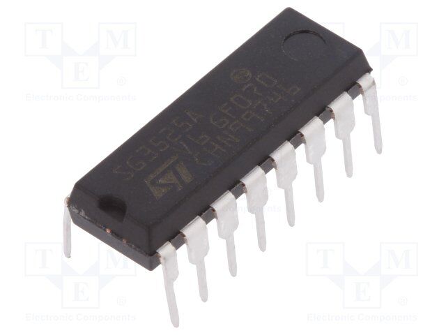
| 封装/外壳 | 16-DIP(0.300",7.62mm) |
| 封装/箱体 | PDIP-16 |
| 工作温度 | 0°C ~ 70°C |
| 工厂包装数量 | 25 |
| 开关频率 | 500 kHz |
| 标准包装 | 25 |
| 电压-电源 | 8 V ~ 35 V |
| 类型 | Voltage Mode PWM Controllers |
| 系列 | SG3525 |
| 输出数 | 2 |
| 输出电压 | 5.2 V |
| 输出端数量 | 2 Output |
| 降压 | 无 |
| 隔离式 | 无 |
| 频率-最大值 | 500kHz |
Datasheet
PDF Datasheet 数据手册内容提取
SG1525A/SG2525A/SG3525A SG1527A/SG2527A/SG3527A Regulating Pulse Width Modulator Description Features The SG1525A/1527A series of pulse width modulator integrated 8V to 35V Operation circuits are designed to offer improved performance and lower 5.1V Reference Trimmed to 1% external parts count when used to implement all types of switching power supplies. The on-chip +5.1 V reference is trimmed to ±1% 100Hz to 500kHz Oscillator Range initial accuracy and the input common-mode range of the error Separate Oscillator Sync Terminal amplifier includes the reference voltage, eliminating external potentiometers and d ivider resistors. A Sync input to the oscillator Adjustable Deadtime Control allows multiple units to be slaved together, or a single unit to be Internal Soft-start synchronized to an external system clock. A single resistor between the C pin and the Di scharge pin provides a wide range of deadtime Input Undervoltage Lockout T adjustment. These d evices also feature built-in soft-start circuitry Latching P.W.M. to Prevent Multiple Pulses with only a timing capacitor required externally. A Shutdown pin controls both the soft -start circuitry and the output stages, providing Dual Source/Sink Output Drivers instantaneous turn-off with soft-start recycle for slow turn-on. These functions are also controlled by an undervoltage lockout which High Reliability Features keeps the outputs o ff and the soft-start capacitor discharged for input voltages less than that required for normal operation. Another Following are the high reliability features of SG1525A unique feature of these PWM circuits is a latch following the and SG1527A: comparator. Once a PWM pulse has been terminated for any reason, the outputs remain off for the duration of the period. The Available to MIL-STD-883, ¶ 1.2.1 latch is reset with each clock pulse. The output stages are totem- MIL-M38510/12602BEA - JAN1525AJ pole designs capabl e of sourcing or sinking in excess of 200mA. The SG1525A output stage features NOR logic, giving a LOW MIL-M38510/12604BEA - JAN1527AJ output for an OFF state. The SG1527A utilizes OR logic, which MSC-AMS level “S” Processing Available results in a HIGH output level when OFF. Block Diagram VREF VC REFERENCE U.V. +VIN REGULATOR LOCKOUT TO GROUND INTERNAL CIRCUITRY OUTPUT A OSC OUTPUT SYNC RT OSCILLATOR Q CT Q OUTPUT B DISCHARGE F/F R SG1525A OUTPUT STAGE P.W.M. + COMPENSATION VIN S LATCH VC INV. INPUT OUTPUT A N.I. INPUT + ERROR AMP 50µA SOFT-SART VREF 5k SHUTDOWN OUTPUT B 5k SG1527A OUTPUT STAGE Figure 1 · Block Diagram September 2014 Rev. 1.4a www.microsemi.com 1 © 2014 Microsemi Corporation
Regulating Pulse Width Modulator Connection Diagrams and Ordering Information Ambient Packaging Type Package Part Number Connection Diagram Temperature Type SG1525AJ-883B SG1525AJ-JAN SG1525AJ-DESC -55°C to SG1525AJ INV. Input 1 16 VR EF N.I. Input 2 15 +VI N 125°C SG1527AJ-883B SYNC 3 14 Output B 16-PIN SG1527AJ-JAN OSC. Output 4 13 V J CERDIP C ceramic DIP SG1527AJ-DESC CT 5 12 Ground R 6 11 Output A SG1527AJ T Discharge 7 10 Shutdown SG2525AJ Soft-start 8 9 Compensation -25°C to 85°C SG2527AJ SG3525AJ N Package: RoHS Compliant / Pb-free -0°C to 70°C Transition DC: 0503 SG3527AJ N Package: RoHS / Pb-free 100% SG2525AN -25°C to 85°C Matte Tin Lead Finish 16-PIN SG2527AN N PDIP plastic DIP SG3525AN -0°C to 70°C SG3527AN SG2525ADW -25°C to 85°C INV. Input 1 16 VR EF SG2527ADW N.I. Input 2 15 +VI N SYNC 3 14 Output B SG3525ADW OSC. Output 4 13 V C 16-pin wide C T 5 12 Ground R 6 11 Output A body T DW SOIC Discharge 7 10 Shutdown plastic Soft-start 8 9 Compensation -0°C to 70°C SOIC SG3527ADW DW Package: RoHS Compliant / Pb- free Transition DC: 0516 DW Package: RoHS / Pb-free 100% Matte Tin Lead Finish SG1525AL-883B 1. N.C. 3 2 1 20 19 11. N.C. 20-pin 2. INV. Input 12. Comp SG1525AL 3. N.I. Input 4 18 13. Shutdown -55°C to ceramic 4. SYNC 5 17 14. Output A 125°C L leadless SG1527AL-883B CLCC 56.. ON.SCC.. Output 6 16 1156.. GN.rCou.nd chip carrier 7. CT 7 15 17. VC (LCC) 98.. DRi Ts charge 8 14 1189.. O+VuI Nt put B SG1527AL 10. Soft-start 9 10 11 12 13 20. VR EF Notes: 1. Contact factory for JAN and DESC product availability. 2. All packages are viewed from the top. 3. Hermetic Packages J & L use Sn63Pb37 hot solder dip lead finish, contact factory for availability of RoHS compliant versions. 2
Absolute Maximum Ratings1 1 Absolute Maximum Ratings Parameter Value Units Supply Voltage (+V ) 40 V IN Collector Supply Voltage (V ) 40 V C Logic Inputs -0.3 to 5.5 V Analog Inputs -0.3 to V V IN Output Current, Source or Sink 500 mA Reference Load Current 50 mA Oscillator Charging Current 5 mA Operating Junction Temperature Hermetic (J, L Packages) 150 °C Plastic (N, DW Packages) 150 °C Storage Temperature Range -65 to 150 °C Lead Temperature (Soldering, 10 seconds) 300 °C RoHS Peak Package Solder Reflow Temp. (40 s max. exp.) 260 (+0, -5) °C Note: Values beyond which damage may occur Thermal Data Parameter Value Units J Package Thermal Resistance-Junction to Case, θ 30 °C/W JC Thermal Resistance-Junction to Ambient, θ 80 °C/W JA N Package Thermal Resistance-Junction to Case, θ 40 °C/W JC Thermal Resistance-Junction to Ambient, θ 65 °C/W JA DW Package Thermal Resistance-Junction to Case, θ 40 °C/W JC Thermal Resistance-Junction to Ambient, θ 95 °C/W JA L Package Thermal Resistance-Junction to Case, θ 35 °C/W JC Thermal Resistance-Junction to Ambient, θ 120 °C/W JA Notes: 1. Junction Temperature Calculation: T = T + (P × θ ). J A D JA 2. The above numbers for θ are maximums for the limiting thermal resistance of the package in a standard mounting JC configuration. The θ numbers are meant to be guidelines for the thermal performance of the device/pc-board system. All of JA the above assume no ambient airflow. 3
Regulating Pulse Width Modulator Recommended Operating Conditions1 Parameter Value Units Input Voltage (+V ) 8 to 35 V IN Collector Voltage (V ) 4.5 to 35 V C Sink/Source Load Current (steady state) 0 to 100 mA Sink/Source Load Current (peak) 0 to 400 mA Reference Load Current 0 to 20 mA Oscillator Frequency Range 0.1 to 350 kHz Oscillator Timing Resistor (R ) 2 to 150 kΩ T Deadtime Resistor Range (R ) 0 to 500 Ω D Maximum Shutdown Source Impedance 5 kΩ Oscillator Timing Capacitor (C ) 0.001 to 0.1 µF T Operating Ambient Temperature Range1 SG1525A/SG1527A -55 to 125 °C SG2525A/SG2527A -25 to 85 °C SG3525A/SG3527A 0 to 70 °C Note: Range over which the device is functional. Electrical Characteristics (Unless otherwise specified, these specifications apply over the operating ambient temperatures for SG1525A/SG1527A with -55°C ≤ T ≤ 125°C, SG2525A/SG2527A with -25°C ≤ T ≤ 85°C, A A SG3525A/SG3527A with 0°C ≤ T ≤ 70°C, and +V = 20V. Low duty cycle pulse testing techniques are A IN used that maintains junction and case temperatures equal to the ambient temperature.) SG1525A/2525A SG3525A Parameter Test Conditions SG1527A/2527A SG3527A Units Min Typ Max Min Typ Max Reference Section1 Output Voltage T = 25C 5.05 5.10 5.15 5.00 5.10 5.20 V J Line Regulation V = 8V to 35V 10 30 10 30 mV IN Load Regulation I = 0 to 20mA 20 50 20 50 mV L Over Operating Temperature Stability1 20 50 20 50 mV Temperature Range Total Output Voltage Over Line, Load and 5.00 5.20 4.95 5.25 V Range1 Temperature Short Circuit Current V = 0V, T = 25C 80 100 80 100 mA REF J 10Hz ≤ f ≤ 10kHz, Vrms Output Noise Voltage1 40 200 40 200 T = 25°C J Long Term Stability1 T = 125C 20 50 20 50 mV/khr J Notes: 1. These parameters, although guaranteed over the recommended operating conditions, are not 100% tested in production. 2. F = 40 kHz (R = 3.6k Ω, C = 0.01µF, R = 0Ω.). OSC T T D 3. Applies to SG1525A/2525A/3525A only, due to polarity of output pulses. 4
Electrical Characteristics (continued) Electrical Characteristics (continued) SG1525A/2525A Parameter Test Conditions SG1527A/2527A SG3525A/SG3527A Units Min Typ Max Min Typ Max Oscillator Section2 Initial Accuracy T = 25C 37.6 40 42.4 37.6 40 42.4 kHz J Voltage Stability V = 8V to 35V ±0.3 ±1 ±1 ±2 % IN Temperature Stability1 MIN ≤ T ≤ MAX ±3 ±6 ±3 ±6 % J Minimum Frequency1 R = 150kΩ, C = 0.1μF 150 150 Hz T T Maximum Frequency1 R = 2 kΩ, C = 1nF 350 350 kHz T T Current Mirror I = 2mA 1.7 2.0 2.2 1.7 2.0 2.2 mA RT Clock Amplitude 3.0 3.5 3.0 3.5 V Clock Width T = 25C 0.3 0.5 1.0 0.3 0.5 1.0 µs J Sync Threshold 1.2 2.0 2.8 1.2 2.0 2.8 V Sync Input Current Sync Voltage = 3.5V 1.0 2.5 1.0 2.5 mA Error Amplifier Section (V = 5.1V) CM Input Offset Voltage 0.5 5 2 10 mV Input Bias Current 1 10 1 10 µA Input Offset Current 1 1 µA DC Open Loop Gain R ≥ 10MΩ, T = 25C 60 75 60 75 dB L J Output Low Level 0.2 0.5 0.2 0.5 V Output High Level 3.8 5.6 3.8 5.6 V Common Mode Rejection V = 1.5V to 5.2 V 60 75 60 75 dB CM Supply Voltage Rejection V = 8V to 35V 50 60 50 60 dB IN PWM Comparator Section2 Minimum Duty Cycle V = 0.6V 0 0 % COMP Maximum Duty Cycle V = 3.6V 45 49 45 49 % COMP Input Threshold2 Zero Duty Cycle 0.6 0.9 0.6 0.9 V Maximum Duty Cycle 3.3 3.6 3.3 3.6 V Input Bias Current 0.05 2.0 0.05 2.0 µA Soft-Start Section Soft Start Current VSHUTDOWN = 0V 25 50 80 25 50 80 µA Soft Start Voltage V = 2V 0.4 0.6 0.4 0.6 V SHUTDOWN Shutdown Input Current V = 2.5V 0.4 1.0 0.4 1.0 mA SHUTDOWN 5
Regulating Pulse Width Modulator SG1525A/2525A Parameter Test Conditions SG1527A/2527A SG3525A/SG3527A Units Min Typ Max Min Typ Max Output Drivers Section (each transistor, V = 20V) C Output High Level I = 20mA 18 19 18 19 V SOURCE I = 100mA 17 18 17 18 V SOURCE Output Low Level I = 20mA 0.2 0.4 0.2 0.4 V SINK I = 100mA 1.0 2.2 1.0 2.2 V SINK Undervoltage Lockout V and V = High 6 7 8 6 7 8 V COMP SS Collector Leakage3 V = 35V 200 200 µA C Rise Time C = 1nF, T = 25°C 100 600 100 600 ns L J Fall Time C = 1nF, T = 25°C 50 300 50 300 ns L J Shutdown Delay1 V = 3V, C = 0, SD S 0.2 0.5 0.2 0.5 µs T = 25°C J Total Standby Current Standby Current VIN = 35V 14 20 14 20 mA Notes: 1. These parameters, although guaranteed over the recommended operating conditions, are not 100% tested in production. 2. F = 40 kHz (R = 3.6k Ω, C = 0.01µF, R = 0Ω). OSC T T D 3. Applies to SG1525A/2525A/3525A only, due to polarity of output pulses. 6
Oscillator Section Oscillator Section VREF 16 Q1 Q5 Q8 7.4k RT 6 Q3 CT 5 Q6 Q9 RAMP 2k 14k TO PWM 2k Q10 Q11 Q14 25k SYNC 3 400µA BLANKING DISCHARGE 7 5 pF TO OUTPUT 23k Q4 Q2 Q7 3k 250 1k 1k Q12 Q13 GND 12 4 CLOCK Figure 2 · Oscillator Schematic 200 500 100 RESISTOR (R) - kΩT 521000 RD = 0C T= 1nFC T= 2nFC T= 5nFC T= .01µCF T= .02µCF T= .05µFC T= 0.1µF ME RESISTOR (R) - ΩD 432000000 C = T1nFC = T2nF C = T5nFC = T.01µFC = .T02µF C = T.05µFC =T 0.1µF TIMING 5 6 5 RD7 DEADTI 100 2 RT CT 0 0 1 2 5 10 20 50 100 200 500 000 000 000 0.2 0.5 1 2 5 10 20 50 100 200 1 2 5 CHARGE TIME - µs DISCHARGE TIME - ms Figure 3 · Oscillator Charge Time versus R And C Figure 4 · Oscillator Discharge Time versus R And C T T D T Oscillator charge time versus R T and C T 7
Regulating Pulse Width Modulator Error Amplifier Section 15 +VIN 80 Q3 B 60 D GAIN - 40 CP = 1nF CP = 0 Q1 Q2 Q4 GE RZ = 20k A ININPVU.T 1 OLT 20 1 - INNP.UI.T 2 COTMoP PAWRAMTOR V 0 2 + 10CP RZ = 0 200 µA 100 µA 5.8 V 30 Ω RZ 9 COMP 1 10 100 1k 10k 100k 1M 10M FREQUENCY - Hz Figure 5 · Error Amplifier Figure 6 · Error Amplifier Open-Loop Frequency Response Output Section +VIN 13 +VC 4 Q5 Q7 VIN = 20 V TA = 25°C Q4 Q9 Q10 3 5k +VREF 1114 OUTPUT Q8 2 Q11 2k Q6 Q1 Q2 Q3 Q6 OMITTED 1 SOURCE SAT. VC - VOH in SG1527A SINK SAT. VOL 5k 10k 10k 0 CLOCK F/F PWM .01 .02 .03 .05 .10 .20 .30 .50 1A Figure 7 · Output Circuit (½ circuit shown) Figure 8 · Output Saturation Characteristics 8
Application Information Application Information +VSUPPLY Q1 TO OUTPUT FILTER +VSUPPLY R1 R1 R2 13 C1 13 +VC A 11 Q1 T1 R2 +VC A 11 SG1525A C2 SG1525A GND B 14 GND B 14 R3 Q2 12 12 RETURN RETURN For single-ended supplies, the driver outputs are In conventional push-pull bipolar designs, forward base grounded. The VC terminal is switched to ground by drive is controlled by R1 - R3 .Rapid turn-off times for the the totem-pole source transistors on alternate power devices are achieved with speed-up capacitors oscillator cycles. C1 and C2. +VSUPPLY R1 +VSUPPLY 13 R1 +VC Q1 13 T1 Q1 C1 A 11 T1 +VC A 11 R1 T2 SG1525A Q2 SG1525A Q2 GND B 14 GND B 14 R2 C2 12 12 RETURN RETURN The low source impedance of the output drivers Low power transformers can be driven directly by the provides rapid charging of power FET input SG1525A. Automatic reset occurs during deadtime, when capacitance while minimizing external components. both ends of the primary winding are switched to ground. 9
Regulating Pulse Width Modulator Shutdown Options 1. Use an external transistor or open-collector comparator to pull down on the Comp terminal. This sets the PWM latch turning off both outputs. If the shutdown signal is momentary, pulse-by-pulse protection can be accomplished as the PWM latch resets with each clock pulse. 2. The same results can be accomplished by pulling down on the Soft-Start terminal with the difference that on this pin, shutdown does not affect the amplifier compensation network but must discharge any Soft-Start capacitor. 3. Apply a positive-going signal to the Shutdown terminal. This provides most rapid shutdown of the outputs but will not immediately set the PWM latch if there is a Soft-Start capacitor. This capacitor discharges but with a current of approximately twice the charging current. 4. The shutdown terminal can be used to set the PWM latch on a pulse-by-pulse basis if there is no external capacitance on Soft-Start terminal. Slow turn-on may still be accomplished by applying an external capacitor, blocking diode, and charging resistor to the comp terminal. (See SG1524 Application Note). VREF 16 RREEGFEURLEANTOCRE 15 +VIN CLOCK 0.1µF 0.1µF FLIP/ 4 FLOP 13 VC 3 kΩ SYNC 0.1µF 3 OUT A PWM RT O ADJ S A 11 10 kΩ C I 6 L 3.6 kΩ RAMP DEADTIME ATL 1k(,2 1) W O 0.009µF 7 R 1.5 100 Ω B 14 kΩ 5 CT OUT B 0.1µF 0.001µF COMP 10 kΩ 12 GND 1 = VOS 9 PWM 23 == II((+-)) 0.01µF 50 µA SOFTSTART 8 + 1 1 5µF 2 2 V/I_ METER 13 31 21 +_E/A 5k 5 k 10 SHUTDOWN VREF 2k + 2 2 2k 3 3 D.U.T Figure 9 · SG1525A/1527A Lab Test Fixture 10
Package Outline Dimensions Package Outline Dimensions Controlling dimensions are in metric, inches equivalents are shown for general information. MILLIMETERS INCHES Dim MIN MAX MIN MAX A 2.06 2.65 0.081 0.104 D A1 0.10 0.30 0.004 0.012 A2 2.03 2.55 0.080 0.100 16 9 B 0.33 0.51 0.013 0.020 c 0.23 0.32 0.009 0.013 H E D 10.08 10.50 0.397 0.413 E 7.40 7.60 0.291 0.299 1 8 e 1.27 BSC 0.05 BSC H 10.00 10.65 0.394 0.419 e L 0.40 1.27 0.016 0.050 B L θ 0° 8° 0° 8° *LC - 0.10 - 0.004 A A2 c *Lead co planarity SEATING PLANE A1 Note: Dimensions do not include protrusions; these shall not exceed 0.155mm (.006”) on any side. Lead dimension shall not include solder coverage. Dimensions are in mm, inches are for reference only. Figure 10 · DW 16-Pin SOWB Package Dimensions MILLIMETERS INCHES Dim MIN MAX MIN MAX A - 5.33 - 0.210 D A1 0.38 - 0.015 - A2 3.30 Typ. 0.130 Typ. E1 b 0.36 0.56 0.014 0.022 1 b1 1.14 1.78 0.045 0.070 b1 c 0.20 0.36 0.008 0.014 E D 18.67 19.69 0.735 0.775 e 2.54 BSC 0.100 BSC A2 A E 7.62 8.26 0.300 0.325 c A1 E1 6.10 7.11 0.240 0.280 L L 2.92 0.381 0.115 0.150 e SEATING PLANE θ θ - 15° - 15° b Note: DFimigeunrseio 1n1s · d o not include protrusions; these shall not exceed 0.155mm (.006”) on any side. Lead dimension shall not include solder coverage. Dimensions are in mm, inches are for reference only. Figure 11 · N 16-Pin Plastic Dual Inline Package Dimensions 11
Regulating Pulse Width Modulator Package Outline Dimensions (continued) Controlling dimensions are in inches, metric equivalents are shown for general information. MILLIMETERS INCHES Dim MIN MAX MIN MAX A - 5.08 - 0.200 b 0.38 0.51 0.015 0.020 D b2 1.04 1.65 0.045 0.065 c 0.20 0.38 0.008 0.015 16 9 D 19.30 19.94 0.760 0.785 E E 5.59 7.11 0.220 0.280 1 8 b2 eA e 2.54 BSC 0.100 BSC eA 7.37 7.87 0.290 0.310 Q A H 0.63 1.78 0.025 0.070 L 3.18 5.08 0.125 0.200 Seating Plane L c α - 15° - 15° H e b θ Q 0.51 1.02 0.020 0.040 Note: Dimensions do not include protrusions; these shall not exceed 0.155mm (.006”) on any side. Lead dimension shall not include solder coverage. Figure 12 · J 16-Pin Ceramic Dual Inline Package Dimensions E3 D MILLIMETERS INCHES Dim MIN MAX MIN MAX D/E 8.64 9.14 0.340 0.360 E3 - 8.128 - 0.320 E e 1.270 BSC 0.050 BSC B1 0.635 TYP 0.025 TYP L 1.02 1.52 0.040 0.060 A 1.626 2.286 0.064 0.090 h 1.016 TYP 0.040 TYP A L2 L A1 8 A1 1.372 1.68 0.054 0.066 A2 - 1.168 - 0.046 3 L2 1.91 2.41 0.075 0.95 B3 0.203R 0.008R Note: 1 All exposed metalized area shall be gold plated 60 micro-inch minimum thickness over nickel 13 plated unless otherwise specified in purchase order. h A2 18 e B3 B1 Figure 13 · L 20-Pin Ceramic LCC Package Outline Dimensions 12
Microsemi Corporation (Nasdaq: MSCC) offers a comprehensive portfolio of semiconductor and system solutions for communications, defense and security, aerospace, and industrial markets. Products include high-performance and radiation-hardened analog mixed-signal integrated circuits, FPGAs, SoCs, and ASICs; power management products; timing and synchronization devices and precise time solutions, setting the world's standard for time; voice processing devices; RF solutions; discrete components; security technologies and scalable anti-tamper products; Power-over-Ethernet ICs and midspans; as well as custom design Microsemi Corporate Headquarters capabilities and services. Microsemi is headquartered in Aliso Viejo, Calif. and has One Enterprise, Aliso Viejo CA 92656 USA Within the USA: +1 (800) 713-4113 approximately 3,400 employees globally. Learn more at www.microsemi.com. Outside the USA: +1 (949) 380-6100 Sales: +1 (949) 380-6136 Fax: +1 (949) 215-4996 © 2014 Microsemi Corporation. All rights reserved. Microsemi and the Microsemi logo are trademarks of E-mail: sales.support@microsemi.com Microsemi Corporation. All other trademarks and service marks are the property of their respective owners. SG1525A/SG1527A.1/09.14