ICGOO在线商城 > 集成电路(IC) > PMIC - 稳压器 - DC DC 切换控制器 > SG3524P
 Datasheet下载
- 型号: SG3524P
- 制造商: STMicroelectronics
- 库位|库存: xxxx|xxxx
- 要求:
| 数量阶梯 | 香港交货 | 国内含税 |
| +xxxx | $xxxx | ¥xxxx |
查看当月历史价格
查看今年历史价格
SG3524P产品简介:
ICGOO电子元器件商城为您提供SG3524P由STMicroelectronics设计生产,在icgoo商城现货销售,并且可以通过原厂、代理商等渠道进行代购。 SG3524P价格参考¥11.39-¥11.39。STMicroelectronicsSG3524P封装/规格:PMIC - 稳压器 - DC DC 切换控制器, 反激,推挽 稳压器 正 输出 升压/降压 DC-DC 控制器 IC 16-SO。您可以下载SG3524P参考资料、Datasheet数据手册功能说明书,资料中有SG3524P 详细功能的应用电路图电压和使用方法及教程。
STMicroelectronics的SG3524P是一款经典的PWM控制器,广泛应用于DC-DC转换器电路中。它属于PMIC(电源管理集成电路)类别中的稳压器和DC-DC切换控制器。该器件主要用于需要精确控制输出电压、电流及频率的开关电源设计。

 应用场景

1. 开关电源(SMPS):
   SG3524P最典型的应用是构建高效、可靠的开关模式电源。它可以用于各种功率范围内的离线式或隔离式DC-DC转换器,如计算机电源、工业控制系统、通信设备等。其双通道误差放大器和可编程振荡器使其能够灵活地适应不同的负载需求,并确保稳定的输出电压。

2. 电池充电器:
   在便携式电子设备中,如手机、平板电脑和其他手持设备的充电器里,SG3524P可以用来实现高效的充电管理。通过调节PWM信号来控制充电电流,确保电池安全快速地充满电,同时保护电池不受过充损害。

3. LED驱动器:
   对于大功率LED照明系统,SG3524P可以作为核心控制芯片,用于恒流源的设计。它能根据外部反馈调整输出电流,从而保证LED亮度的一致性和稳定性,适用于路灯、汽车前照灯等领域。

4. 电机驱动:
   在某些小型电机驱动应用中,SG3524P也可以发挥重要作用。例如,在风扇、泵浦或其他低功耗电机的驱动电路中,利用其PWM功能来调速,既节能又能延长电机寿命。

5. 其他专用电源模块:
   除了上述常见应用外,SG3524P还适合用于定制化的电源解决方案,如实验室仪器、医疗设备等对电源精度要求较高的场合。它提供的高精度参考电压、软启动功能以及完善的保护机制(如过流、短路保护),使得这些特殊应用更加可靠。

总之,SG3524P凭借其高性能和多功能性,成为众多电力电子领域不可或缺的关键组件之一。
| 参数 | 数值 |
| 产品目录 | 集成电路 (IC)半导体 |
| Cuk | 无 |
| 描述 | IC REG CTRLR FLYBK DBLR 16SOIC开关控制器 Regulated Volt Mode |
| 产品分类 | |
| 品牌 | STMicroelectronics |
| 产品手册 | |
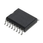
| 产品图片 |
|
| rohs | 过渡期间无铅 / 符合限制有害物质指令(RoHS)规范要求 |
| 产品系列 | 电源管理 IC,开关控制器 ,STMicroelectronics SG3524P- |
| 数据手册 | |
| 产品型号 | SG3524P |
| PWM类型 | 电压模式 |
| 上升时间 | 200 ns |
| 下降时间 | 100 ns |
| 产品培训模块 | http://www.digikey.cn/PTM/IndividualPTM.page?site=cn&lang=zhs&ptm=26258 |
| 产品目录页面 | |
| 产品种类 | 开关控制器 |
| 倍增器 | 是 |
| 其它名称 | 497-5377-5 |
| 其它有关文件 | http://www.st.com/web/catalog/sense_power/FM142/CL1454/SC352/PF64202?referrer=70071840 |
| 分频器 | 无 |
| 包装 | 管件 |
| 升压 | 无 |
| 占空比 | 45% |
| 占空比-最大 | 45 % |
| 反向 | 无 |
| 反激式 | 是 |
| 同步管脚 | No |
| 商标 | STMicroelectronics |
| 安装风格 | SMD/SMT |
| 封装 | Tube |
| 封装/外壳 | 16-SOIC(0.154",3.90mm 宽) |
| 封装/箱体 | SO-16 |
| 工作温度 | 0°C ~ 70°C |
| 工厂包装数量 | 50 |
| 开关频率 | 300 kHz |
| 拓扑结构 | Push-Pull |
| 最大工作温度 | + 70 C |
| 最小工作温度 | 0 C |
| 标准包装 | 50 |
| 电压-电源 | 8 V ~ 40 V |
| 类型 | Voltage Mode PWM Controllers |
| 系列 | SG3524 |
| 输出数 | 1 |
| 输出电压 | 18 V |
| 输出电流 | 100 mA |
| 输出端数量 | 2 Output |
| 降压 | 无 |
| 隔离式 | 无 |
| 频率-最大值 | 300kHz |


- 商务部:美国ITC正式对集成电路等产品启动337调查
- 曝三星4nm工艺存在良率问题 高通将骁龙8 Gen1或转产台积电
- 太阳诱电将投资9.5亿元在常州建新厂生产MLCC 预计2023年完工
- 英特尔发布欧洲新工厂建设计划 深化IDM 2.0 战略
- 台积电先进制程称霸业界 有大客户加持明年业绩稳了
- 达到5530亿美元!SIA预计今年全球半导体销售额将创下新高
- 英特尔拟将自动驾驶子公司Mobileye上市 估值或超500亿美元
- 三星加码芯片和SET,合并消费电子和移动部门,撤换高东真等 CEO
- 三星电子宣布重大人事变动 还合并消费电子和移动部门
- 海关总署:前11个月进口集成电路产品价值2.52万亿元 增长14.8%


PDF Datasheet 数据手册内容提取
SG3524 ® REGULATING PULSE WIDTH MODULATORS COMPLETE PWM POWER CONTROL CIR- CUITRY UNCOMMITTED OUTPUTS FOR SINGLE- ENDED OR PUSH PULL APPLICATIONS LOW STANDBY CURRENT 8mA TYPICAL OPERATION UP TO 300KHz 1% MAXIMUM TEMPERATURE VARIATION OF REFERENCE VOLTAGE DESCRIPTION DIP16 SO16 The SG3524 incorporates on a single monolithic ORDERING NUMBERS: SG3524N (DIP16) chip all the function required for the construction SG3524P (SO16) of regulating power suppies inverters or switching regulators. They can also be used as the control element for high power-output applications. The SG3524 family was designed for switching regu- lators of either polarity, transformer-coupled dc- to-dc converters, transformerless voltage dou- Each device includes an on-ship reference, error blers and polarity converter applications amplifier, programmable oscillator, pulse-steering employing fixed-frequency, pulse-width modula- flip flop, two uncommitted output transistors, a tion techniques. The dual alternating outputs al- high-gain comparator, and current-limiting and lows either single-ended or push-pull applications. shut-down circuitry. BLOCK DIAGRAM July 2000 1/9 This is advanced information on a new product now in development or undergoing evaluation. Details are subject to change without notice.
SG3524 ABSOLUTE MAXIMUM RATINGS Symbol Parameter Value Unit VIN Supply Voltage 40 V IC Collector Output Current 100 mA IR Reference Output Current 50 mA IT Current Through CT Terminal – 5 mA Ptot Total Power Dissipation at Tamb = 70(cid:176) C 1000 mW Tstg Storage Temperature Range – 65 to 150 (cid:176) C Top Operating Ambient Temperature Range: 0 to 70 (cid:176) C PIN CONNECTION (Top view) THERMAL DATA Symbol Parameter DIP16 SO16 Unit Rth j-amb Thermal Resistance Junction-ambient Max. 80 – (cid:176) C/W Rth j-alumina Thermal Resistance Junction-alumina (*) Max. – 50 (cid:176) C/W (*) Thermal resistance junction-alumina with the device soldered on the middle of an alumina supporting substrate measuring 15 x 20mm; 0.65mm thickness with infinite heatsink. 2/9
SG3524 ELECTRICAL CHARACTERISTICS (unless otherwise stated, these specifications apply for Tj = 0 to 70(cid:176) C, VIN = 20V, and f = 20KHz). Symbol Parameter Test Condition Min. Typ. Max. Unit REFERENCE SECTION VREF Output Voltage 4.6 5 5.4 V D VREF Line Regulation VIN = 8 to 40V 10 30 mV D VREF Load Regulation IL = 0 to 20mA 20 50 mV Ripple Rejection f = 120Hz, Tj = 25(cid:176) C 66 dB Short Circuit Current Limit VREF = 0, Tj = 25(cid:176) C 100 mA D VREF/D T Temperature Stability Over Operating Temperature range 0.3 1 % D VREF Long Term Stability Tj = 125(cid:176) C, t = 1000Hrs 20 mV OSCILLATOR SECTION fMAX Maximum Frequency CT = 0.001m F, RT = 2KW 300 KHz Initial Accuracy RT and CT Constant 5 % Voltage Stability VIN = 8 to 40V, Tj = 25(cid:176) C 1 % D f/D T Temperature Stability Over Operating Temperature Range 2 % Output Amplitude Pin 3, Tj = 25(cid:176) C 3.5 V Output Pulse Width CT = 0.01m F, Tj = 25(cid:176) C 0.5 m s ERROR AMPLIFIER SECTION VOS Input Offset Voltage VCM = 2.5V 2 10 mV Ib Input Bias Current 2 10 m A GV Open Loop Voltage Gain 60 80 dB CMV Common Mode Voltage Tj = 25(cid:176) C 1.8 3.4 V CMR Common Mode Rejection Tj = 25(cid:176) C 70 dB B Small Signal Bandwidth AV = 0dB, Tj = 25(cid:176) C 3 MHz VO Output Voltage Tj = 25(cid:176) C 0.5 3.8 V COMPARATOR SECTION Duty-cycle % Each Output On 0 45 % VIT Input Threshold Zero Duty-cycle 1 V Maximum Duty-cycle 3.5 V Ib Input Bias Current 1 m A CURRENT LIMITING SECTION Sense Voltage Pin 9 = 2V with Error Amp. Set for 180 200 220 mV Max. Out. Tj = 25(cid:176) C Sense Voltage T.C. 0.2 mV/(cid:176) C CMV Common Mode Voltage –1 1 OUTPUT SECTION(each output) Collector-emitter Voltage 40 V Collector Leackage Curr. VCE = 40V 0.1 50 m A Saturation Voltage IC = 50mA 1 2 V Emitter Output Voltage VIN = 20V 17 18 V tr Rise Time RC = 2KW , Tj = 25(cid:176) C 0.2 m s tf Fall Time RC = 2KW , Tj = 25(cid:176) C 0.1 m s Iq (*) Total Standby Current VIN = 40V 8 10 mA (*) Excluding oscillator charging current, error and current limit dividers, and with outputs open. 3/9
SG3524 Figure 1: Open-loop Voltage Amplification of Figure 2: Oscillator Frequency vs. Timing Error Amplifier vs. Frequency Components. Figure 3: Output Dead Time vs. Timing Figure 4: Output Saturation Voltage vs. load Capacitance Value. Current. Figure 5: Open Loop Test Circuit. 4/9
SG3524 cording to the approximate formula: PRINCIPLES OF OPERATION The SG3524 is a fixed frequency pulse-with- 1.18 modulation voltage regulator control circuit. The f = R C regulator operates at a frequency that is pro- T T grammed by one timing resistor (RT) and one tim- where: civnhogalt argcgiaenp gra accmiutoprrr e an(t CtC TfTo).,r wRChTTi c. heT shistia sfb elrdies hstoue ldttsh eai n c coaom nlpisnatearaanr-t RCTT iiss iinn Km FW f is in KHz tor providing linear control of the output pulse width by the error amplifier. the SG3524 contains, Pratical values of CT fall between 0.001 and an on-board 5V regulator that serves as a refer- 0.1m F. Pratical values of RT fall between 1.8 and ence as well as powering the SG3524’s internal 100KW . This results in a frequency range typically control circuitry and is also useful in supplying ex- from 120Hz to to 500KHz. ternal support functions. This reference voltage is lowered externally by a resistor divider to provide a reference within the common mode range the BLANKING error amplifier or an external reference may be The output pulse of oscillator is used as a blank- used. The power supply output is sensed by a ing pulse at the output. This pulse width is con- second resistor divider network to generale a trolled by the value of CT.If small values of CT are feedback signal to error amplifier. The amplifier required for frequency control, the oscillator out- output voltage is then compared to the linear volt- put pulse width may still be increased by applying age ramp at CT. The resulting modulated pulse a shunt capacitance of up to 100pF from pin 3 to out of the high-gain comparator is then steered to ground. If still greater dead-time is required, it the appropriate output pass transistors (QA or QB) should be accomplished by limiting the maximum by the pulse-steering flip-flop, which is synchro- duty cycle by clamping the output of the error am- nously toggled by the oscillator output. The oscil- plifier. This can easily be done with the circuit be- lator output pulse also serves as a blanking pulse low: to assure both output are never on simultane- ously during the transition times. The width of the blanking pulse is controlled by the value of CT. Figure 6. The outputs may be applied in a push-pull con- figuration in which their frequency is half that of the base oscillator, or paralleled for single-ended applications in which the frequency is equal to that of the oscillator. The output of the error am- plifier shares a common input to the comparator with the current limiting at shutdown circuitry and can be overridden by signals from either of these inputs. This common point is also available exter- nally and may be employed to control the gain of, or to compensate, the error amplifier, or to pro- SYNCRONOUS OPERATION vide additional control to the regulator. When an external clock is desired, a clock pulse of approximately 3V can be applied directly to the RECOMMENDED OPERATING CONDITIONS oscillator output terminal. The impedance to ground at this point is approximately 2KW . In this Supply voltage VIN 8 to 40V configuration RT CT must be selected for a clock Reference Output Current 0 to 20mA period slightly greater than that the external clock. Current trough CT Terminal - 0.03 to -2mA If two more SG2524 regulators are to be operated TTiimmiinngg CRaepsiasctoitro, rR, CTT 01.0.80 1to t o1 000.1KmW F nssyhenocctuehlddro tnbooe au stsileiyn,dg letao ltlg imetoihnsegcr i,lcl aaatpolla r cCitoTo ur,tt peaurnmtd i nttiaemlrsmin gicn oarnels-- sistor connected to a single RT terminal. The TYPICAL APPLICATIONS DATA other RT terminals can be left open or shorted to VREF. Minimum lead lengths should be used be- OSCILLATOR tween the CT terminals. The oscillator controls the frequency of the SG3524 and is programmed by RT and CT ac- 5/9
SG3524 Figure 7: Flyback Converter Circuit. Figure 8: PUSH-PULL Transformer-coupled circuit. 6/9
SG3524 mm inch OUTLINE AND DIM. MECHANICAL DATA MIN. TYP. MAX. MIN. TYP. MAX. a1 0.51 0.020 B 0.77 1.65 0.030 0.065 b 0.5 0.020 b1 0.25 0.010 D 20 0.787 E 8.5 0.335 e 2.54 0.100 e3 17.78 0.700 F 7.1 0.280 I 5.1 0.201 L 3.3 0.130 DIP16 Z 1.27 0.050 7/9
SG3524 mm inch DIM. OUTLINE AND MIN. TYP. MAX. MIN. TYP. MAX. MECHANICAL DATA A 1.75 0.069 a1 0.1 0.25 0.004 0.009 a2 1.6 0.063 b 0.35 0.46 0.014 0.018 b1 0.19 0.25 0.007 0.010 C 0.5 0.020 c1 45˚ (typ.) D (1) 9.8 10 0.386 0.394 E 5.8 6.2 0.228 0.244 e 1.27 0.050 e3 8.89 0.350 F (1) 3.8 4 0.150 0.157 G 4.6 5.3 0.181 0.209 L 0.4 1.27 0.016 0.050 M 0.62 0.024 SO16 Narrow S 8˚(max.) (1) D and F do not include mold flash or protrusions. Mold flash or potrusions shall not exceed 0.15mm (.006inch). 8/9
SG3524 Information furnished is believed to be accurate and reliable. However, STMicroelectronics assumes no responsibility for the consequences of use of such information nor for any infringement of patents or other rights of third parties which may result from its use. No license is granted by implication or otherwise under any patent or patent rights of STMicroelectronics. Specification mentioned in this publication are subject to change without notice. This publication supersedes and replaces all information previously supplied. STMicroelectronics products are not authorized for use as critical components in life support devices or systems without express written approval of STMicroelectronics. The ST logo is a registered trademark of STMicroelectronics © 2000 STMicroelectronics – Printed in Italy – All Rights Reserved STMicroelectronics GROUP OF COMPANIES Australia - Brazil - China - Finland - France - Germany - Hong Kong - India - Italy - Japan - Malaysia - Malta - Morocco - Singapore - Spain - Sweden - Switzerland - United Kingdom - U.S.A. http://www.st.com 9/9