ICGOO在线商城 > 晶体,振荡器,谐振器 > 可编程振荡器 > SG-8002CA-STB
 Datasheet下载
- 型号: SG-8002CA-STB
- 制造商: EPSON
- 库位|库存: xxxx|xxxx
- 要求:
| 数量阶梯 | 香港交货 | 国内含税 |
| +xxxx | $xxxx | ¥xxxx |
查看当月历史价格
查看今年历史价格
SG-8002CA-STB产品简介:
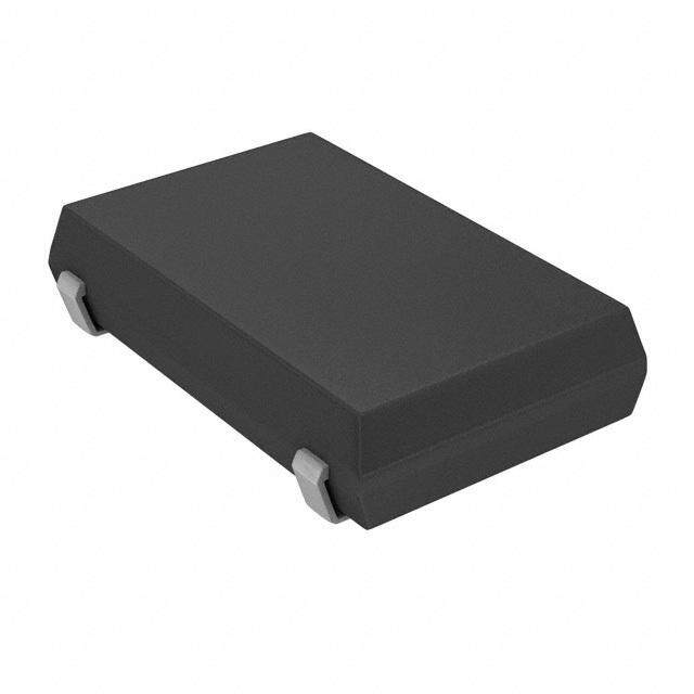
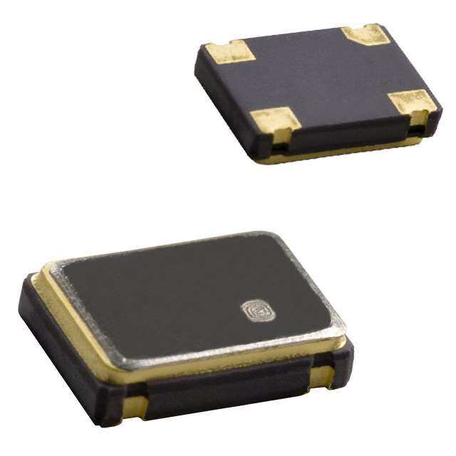
ICGOO电子元器件商城为您提供SG-8002CA-STB由EPSON设计生产,在icgoo商城现货销售,并且可以通过原厂、代理商等渠道进行代购。 SG-8002CA-STB价格参考。EPSONSG-8002CA-STB封装/规格:可编程振荡器, XO (Standard) TTL 1MHz ~ 125MHz Programmable Oscillator 5V Standby 4-SMD, No Lead。您可以下载SG-8002CA-STB参考资料、Datasheet数据手册功能说明书,资料中有SG-8002CA-STB 详细功能的应用电路图电压和使用方法及教程。
EPSON品牌的SG-8002CA-STB是一款可编程振荡器,其应用场景主要集中在需要高精度时钟信号和灵活频率配置的电子设备中。以下是该型号的具体应用场景:

1. 通信设备:
   SG-8002CA-STB适用于各种通信设备,如路由器、交换机、基站模块等。它能够提供稳定的时钟信号,支持数据传输的同步需求,并可根据具体应用调整输出频率。

2. 消费类电子产品:
   在智能电视、音视频播放器、游戏机等消费类电子产品中,这款振荡器可用于音频/视频同步、处理器时钟源等场景,确保设备运行的稳定性和精确性。

3. 工业自动化:
   工业控制设备(如PLC、传感器模块、数据采集系统)需要可靠的时钟信号来保证实时性和准确性。SG-8002CA-STB的可编程特性使其能够适应不同工业设备的需求。

4. 计算机与存储设备:
   在硬盘驱动器、固态硬盘(SSD)、RAID控制器等存储设备中,这款振荡器可以作为主时钟或参考时钟,为数据读写操作提供精准的时间基准。

5. 医疗设备:
   医疗仪器(如心电图仪、超声波设备、监护仪)对时钟信号的要求非常高。SG-8002CA-STB的低相位噪声和高稳定性特点非常适合这些应用。

6. 汽车电子:
   汽车信息系统、导航系统和驾驶辅助系统中,需要高性能的时钟源以支持复杂的计算和实时处理任务。SG-8002CA-STB能够在宽温度范围内保持稳定工作,满足车载环境的需求。

7. 物联网(IoT)设备:
   在智能家居、可穿戴设备和其他IoT终端中,这款振荡器可用于微控制器、无线模块和传感器接口的时钟驱动,同时其低功耗特性有助于延长电池寿命。

总结来说,EPSON SG-8002CA-STB凭借其高精度、可编程性和良好的环境适应能力,在通信、工业、消费电子、医疗、汽车以及物联网等领域有着广泛的应用价值。
| 参数 | 数值 |
| 产品目录 | 晶体和振荡器 |
| 描述 | OSCILLATOR TTL PROG 5V ST SMD |
| 产品分类 | |
| 品牌 | EPSON |
| 数据手册 | |
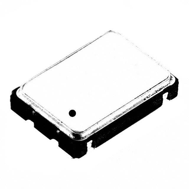
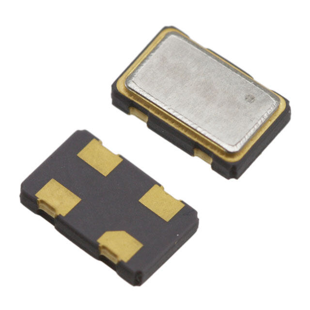
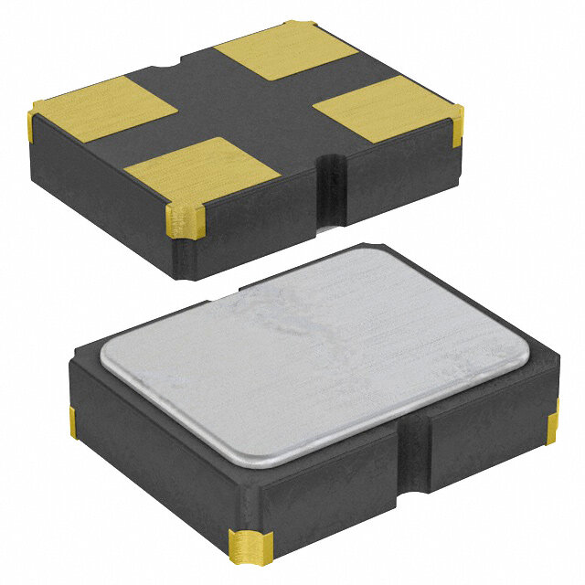
| 产品图片 |
|
| 产品型号 | SG-8002CA-STB |
| rohs | 无铅 / 符合限制有害物质指令(RoHS)规范要求 |
| 产品系列 | SG-8002CA |
| 产品培训模块 | http://www.digikey.cn/PTM/IndividualPTM.page?site=cn&lang=zhs&ptm=25398 |
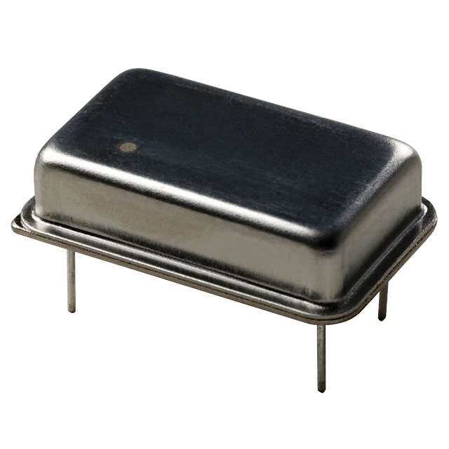
| 产品目录绘图 |
|
| 产品目录页面 | |
| 功能 | 待机 (断电) |
| 包装 | 管件 |
| 可用频率范围 | 1MHz ~ 125MHz |
| 大小/尺寸 | 0.276" 长 x 0.197" 宽(7.00mm x 5.00mm) |
| 安装类型 | 表面贴装 |
| 封装/外壳 | 4-SMD,无引线(DFN,LCC) |
| 工作温度 | -20°C ~ 70°C |
| 扩频带宽 | - |
| 标准包装 | 1 |
| 电压-电源 | 5V |
| 电流-电源(最大值) | 45mA |
| 电流-电源(禁用)(最大值) | 50µA |
| 类型 | 由 Digi-Key 编程(请在网站订购单中输入您需要的频率) |
| 输出 | TTL |
| 频率稳定度 | ±50ppm |
| 高度 | 0.055"(1.40mm) |


- 商务部:美国ITC正式对集成电路等产品启动337调查
- 曝三星4nm工艺存在良率问题 高通将骁龙8 Gen1或转产台积电
- 太阳诱电将投资9.5亿元在常州建新厂生产MLCC 预计2023年完工
- 英特尔发布欧洲新工厂建设计划 深化IDM 2.0 战略
- 台积电先进制程称霸业界 有大客户加持明年业绩稳了
- 达到5530亿美元!SIA预计今年全球半导体销售额将创下新高
- 英特尔拟将自动驾驶子公司Mobileye上市 估值或超500亿美元
- 三星加码芯片和SET,合并消费电子和移动部门,撤换高东真等 CEO
- 三星电子宣布重大人事变动 还合并消费电子和移动部门
- 海关总署:前11个月进口集成电路产品价值2.52万亿元 增长14.8%
PDF Datasheet 数据手册内容提取
Crystal oscillator CRYSTAL OSCILLATOR Product Number (please contact us) PROGRAMMABLE OUTPUT : CMOS CE, CA SG - 8002 series Frequency range : 1 MHz to 125 MHz CE CA Supply voltage : 3.0 V / 3.3 V / 5.0 V Function : Output enable(OE) or Standby(ST) Short mass production lead time by PLL technology. SG-Writer available to purchase, please contact Epson or local sales representative. DC JA JC Specifications (characteristics) Specifications *2 Item Symbol Conditions / Remarks PT / ST PH / SH PC / SC 1 MHz to 125 MHz - VCC = 4.5 V to 5.5 V Output frequency range f0 - - 1 MHz to 125 MHz VCC = 3.0 V to 3.6 V - - 1 MHz to 66.7 MHz VCC = 2.7 V to 3.6 V Supply voltage VCC 4.5 V to 5.5 V 2.7 V to 3.6 V -55 C to +125 °C (SG-8002CA / JA / DC ) Storage temperature T_stg -55 C to +100 °C (SG-8002JC) Storage as single product. -40 C to +125 °C (SG-8002CE) Operating temperature*1 T_use -20 C to +70 °C / -40 C to +85 °C B: 50 10-6, C: 100 10-6 -20 C to +70 C Frequency tolerance f_tol M: 100 10-6 M: 100 10-6 -40 C to +85 C (except SG-8002JC) *3 40 mA Max. (SG-8002CE) Current consumption ICC 45 mA Max. 28 mA Max. No load condition, Max. frequency (SG-8002CA / JC / JA / DC ) Output disable current I_dis 30 mA Max. 16 mA Max. OE=GND (PT.PH,PC) Stand-by current I_std 50 µA Max. ST=GND (ST,SH,SC) 40 % to 60 % - TTL load: 1.4 V, Max. load condition Symmetry *1 SYM 45 % to 55 % - 40 % to 60 % CMOS load:50 % VCC level, Max. load condition - 45 % to 55 % VOH VCC -0.4 V Min. IOH=-16 mA (PT,ST,PH,SH ) , -8 mA (PC,SC) Output voltage VOL 0.4 V Max. IOL=16 mA (PT,ST,PH,SH) , 8 mA (PC,SC) Max. frequency and Max. Supply voltage 5 TTL Max. - Output load condition (SG-8002CE / CA / JA / DC ) L_TTL (TTL) *1 5 TTL Max. - f0 90 MHz and Max. Supply voltage (SG-8002JC ) Max. frequency and Max. Supply voltage 15 pF Max. Output load condition (SG-8002CE / JC) L_CMOS (CMOS) *1 Max. frequency and Max. Supply voltage 15 pF Max. 25 pF Max 15 pF Max. (SG-8002CA / JA / DC ) Input voltage VIH 2.0 V Min. 70 % VCC Min. OE terminal orSTterminal VIL 0.8 V Max. 20 % VCC Max. 4 ns Max. - TTL load: 0.4 V to 2.4 V level Rise / Fall time *1 tr/ tf - 3 ns Max. CMOS load: 20 % VCC to 80 % VCC level Start-up time t_str 10 ms Max. Time at minimum supply voltage to be 0 s Frequency aging f_aging ±5 × 10⁻⁶ / year Max. +25 C, VCC=5.0 V/ 3.3 V (PC,SC) First year *1 Please refer to “Outline specifications” page for information regarding; operating temperature, available frequencies, symmetry, output load condi- tions and rise/fall time. *2 Please refer to “Jitter specifications and characteristics chart” page for PLL-PLL connection & Jitter specification. *3 Please refer to “Outline specifications” for availability of tolerance “M”. A “Frequency checking” program on the Seiko Epson website is also available.
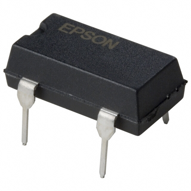
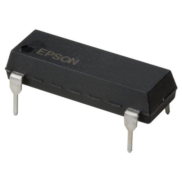
Crystal oscillator External dimensions and Recommended footprint (Unit:mm) SG-8002CE Ceramic SON 4pin 3.2x2.5x1.05 mm 3.20.2 C (ex.0.01 µF) 2.2 #4 #3 #3 #4 1.4 E125.0C 0.2 9 #4 #3 SC181A 2.5 0.0.7 1.2 #1 #2 5 #2 0.9 #1 1.9 1 0. 5 0 1. #1 #2 2.4 Resist SG-8002CA Ceramic SON 4pin 7.0x5.0x1.4 mm 1.8 1.4 C #4 #3 #3 #4 (ex. 0.01 μF) 0 E P12H5C.903050C ±0.25.0 2.6 2. 4.2 #1 7.0±0.2 #2 #2 5.08 #1 Resist +0.1 4 -0.15 5.08 1. 5.08 SG-8002JC SOJ 4pin 10.5x5.8x2.7 mm Package and pin compatible with SG-636. 10.5 Max. #4 #3 1.3 The metal case inside of the molding com- 2EP1H2 5 9.0305070B C 5.0 5.8 Max. poTeoffhf eutihscn itsdp o upmnrre oaqldyyuu abccloeitt.ys e,m rxeepltoiiacsb eaidlnit dyo nod rot heeelse ctnotropict aohlra svbpeoe tctaosnm.y 2.1 #1 #2 4.6 x. Ma 7 0.51 5.08 2.(1.0) (1.0) 5.08 0.05Min. 3.6 Note. OE Pin (PT, PH, PC) Pin map To maintain stable operation, provide a OE Pin = "H" or "open": Specified frequency output. Pin Connection 0.01uF to 0.1uF by-pass capacitor at a loca- OE Pin = "L": Output is high impedance. 1 OE or ST tion as near as possible to the power source ST Pin (ST, SH, SC) 2 GND tGeNrmDi)n.a l of the crystal product (between VCC - ST Pin = "H" or "open": Specified frequency output. 3 OUT ST Pin = "L": Output is low level (weak pull - down), oscillation 4 VCC stops.
Crystal oscillator External dimensions and Recommended footprint (Continued) (Unit:mm) SG-8002JA SOJ 4pin 14.0x9.8x4.7 mm Package and pin compatible with SG-615. 14.0 Max. #4 #3 1.3 EPSON x. 120P0H.0 0903057 CB 8.65 9.8 Ma 3.0 8.8 #1 #2 x. Ma 5 0.51 4.7 0.2 5.08 7.62 5.08 0.25Min. SG-8002DC DIP half size #8 #5 EPSON 100.0000 C 6 2PH 9357B 6. #1 13.7 Max. #4 x. 7.62 a M 3 5. n. 0.25 0.2Min. Mi 0.51 4 90~105 7.62 2.5 Note. OE Pin (PT, PH, PC) Pin map Pin map: SG-8002DC OE Pin = "H" or "open": Specified frequency output. Pin Connection Pin Connection OE Pin = "L": Output is high impedance. 1 OE or ST 1 OE or ST 2 GND 4 GND ST Pin (ST, SH, SC) 3 OUT 5 OUT ST Pin = "H" or "open": Specified frequency output. 4 VCC 8 VCC ST Pin = "L": Output is low level (weak pull - down), oscillation stops. To maintain stable operation, provide a 0.01uF to 0.1uF by-pass capacitor at a location as near as possible to the power source terminal of the crys- tal product (between Vcc - GND). Products number (Please contact us for each product.) SG-8002CE: Q3321CExxxxxx00 SG-8002JC: Q3307JCx2xxxx00 SG-8002CA: Q3309CAx0xxxx00 SG-8002DC: Q3204DCx2xxxx00 SG-8002JA: Q3306JAx2xxxx00
Crystal oscillator SG-8002 Series Outline of specifications Supply Model vaoglet- teOmppeeraratitnugre Ocuotpndutit ilooand Symmetry OOuutptpuut tr ifsaell ttiimmee / 40 % to 60 % (1.4 V, L_TTL=5 TTL+15 pF, f0≤125 MHz) -20 °C to +70 °C 2.0 ns Max. (0.8 V to 2.0 V,L_TTL=Max.) PT/ST 5TTL+15pF 45 % to 55 % (1.4 V, L_TTL=5 TTL+15 pF, f0≤66.7 MHz) 4.0 ns Max. (0.4 V to 2.4 V,L_TTL=Max.) 4.5 V to -40 °C to +85 °C 45 % to 55 % (1.4 V, L_TTL=5 TTL+15 pF, f0≤27.0 MHz) 5.5 V 15 pF (f0≤125 MHz) 40 % to 60 % (50 % VCC, L_CMOS=15 pF, f0≤125 MHz) -20 °C to +70 °C PH/SH 25 pF (f0≤100 MHz) 45 % to 55 % (50 % VCC, L_CMOS=25 pF, f0≤66.7 MHz) 3.0 ns Max. (20 % VCC to 80 % VCC,L_CMOS=Max.) SG-8002CE -40 °C to +85 °C 25 pF (f0≤27 MHz) 45 % to 55 % (50 % VCC, L_CMOS=25 pF, f0≤27.0 MHz) 3.0 V to 40 % to 60 % (50 % VCC, L_CMOS=15 pF, f0≤125 MHz) 3.6 V 45 % to 55 % (50 % VCC, L_CMOS=15 pF, f0≤40 MHz) PC/SC -40 °C to +85 °C 15 pF 3.0 ns Max. (20 % VCC to 80 % VCC,L_CMOS=Max.) 2.7 V to 40 % to 60 % (50 % VCC, L_CMOS=15 pF, f0≤66.7 MHz) 3.6 V 40 % to 60 % (1.4 V, L_TTL=5 TTL+15 pF, f0≤125 MHz) 5TTL+15pF (f0≤125 MHz) -20 °C to +70 °C ↑ (1.4 V, L_CMOS=25 pF, f0≤66.7 MHz) 25 pF (f0≤66.7 MHz) 2.0 ns Max. (0.8 V to 2.0 V,L_CMOS or L_TTL=Max.) PT/ST 45 % to 55 % (1.4 V, L_TTL=5 TTL+15 pF, f0≤66.7 MHz) 4.0 ns Max. (0.4 V to 2.4 V,L_CMOS or L_TTL=Max.) 5 TTL+15 pF (f0≤40 MHz) 40 % to 60 % (1.4 V, L_CMOS=15 pF, f0≤55.0 MHz) -40 °C to +85 °C SG-8002CA 4.5 V to 15 pF (f0≤55 MHz) 45 % to 55 % (1.4 V, L_TTL=5 TTL+15 pF, f0≤40.0 MHz) 5.5 V 40 % to 60 % (50 % VCC, L_CMOS=25 pF, f0≤125 MHz) 25 pF (f0≤125 MHz) SG-8002JA -20 °C to +70 °C ↑ (50 % VCC, L_CMOS=50 pF, f0≤66.7 MHz) 50 pF (f0≤66.7 MHz) 3.0 ns Max. (20 % VCC to 80 % VCC,L_CMOS≤25pF) PH/SH 45 % to 55 % (50 % VCC, L_CMOS=25 pF, f0≤66.7 MHz) 4.0 ns Max. (20 % VCC to 80 % VCC,L_CMOS=Max.) SG-8002DC 15 pF (f0≤55 MHz) 40 % to 60 % (50 % VCC, L_CMOS=15 pF, f0≤55.0 MHz) -40 °C to +85 °C 25 pF (f0≤40 MHz) 45 % to 55 % (50 % VCC, L_MOS=25 pF, f0≤40.0 MHz) 3.0 V to 15 pF 40 % to 60 % (50 % VCC, L_CMOS=15 pF, f0≤125 MHz) 3.6 V 30 pF (f0≤40 MHz) 45 % to 55 % (50 % VCC, L_CMOS=30 pF, f0≤40 MHz) 3.0 ns Max. (20 % VCC to 80 % VCC,L_CMOS≤15pF) PC/SC 2.7 V to -40 °C to +85 °C 4.0 ns Max. (20 % VCC to 80 % VCC,L_CMOS=Max.) 15 pF 40 % to 60 % (50 % VCC, L_CMOS=15 pF, f0≤66.7 MHz) 3.6 V 40 % to 60 % (1.4 V,L_CMOS=15 pF, f0≤125 MHz) 5TTL+15 pF (f0≤90 MHz) ↑ (1.4 V,L_TTL=5 TTL+15 pF, f0≤90.0 MHz) 2.0 ns Max. (0.8 V to 2.0 V,L_CMOS or L_TTL=Max.) PT/ST 15 pF (f0≤125 MHz) ↑ (1.4 V,L_CMOS=25 pF, f0≤66.7 MHz) 4.0 ns Max. (0.4 V to 2.4 V,L_CMOS or L_TTL=Max.) 25 pF (f0≤66.7 MHz) 4.5 V to 45 % to 55 % (1.4 V,L_TTL=5 TTL+15 pF, f0≤66.7 MHz) -20 °C to +70 °C 5.5 V 40 % to 60 % (50 % VCC, L_CMOS=15 pF, f0≤125 MHz) 15 pF (f0≤125 MHz) ↑ (50 % VCC, L_CMOS=25 pF, f0≤90 MHz) 3.0 ns Max. (20 % VCC to 80 % VCC,L_CMOS≤25pF) SG-8002JC PH/SH 25 pF (f0≤90 MHz) ↑ (50 % VCC, L_CMOS=50 pF, f0≤50 MHz) 4.0 ns Max. (20 % VCC to 80 % VCC,L_CMOS=Max.) 50 pF (f0≤66.7 MHz) 45 % to 55 % (50 % VCC, L_CMOS=25 pF, f0≤66.7 MHz) 3.0 V to 15 pF 40 % to 60 % (50 % VCC, L_CMOS=15 pF, f0≤125 MHz) 3.6 V 30 pF (f0≤40 MHz) 45 % to 55 % (50 % VCC, L_CMOS=30 pF, f0≤40 MHz) 3.0 ns Max. (20 % VCC to 80 % VCC,L_CMOS≤15pF) PC/SC -20 °C to +70 °C 2.7 V to 4.0 ns Max. (20 % VCC to 80 % VCC,L_CMOS=Max.) 15 pF 40 % to 60 % (50 % VCC, L_CMOS=15 pF, f0≤66.7 MHz) 3.6 V Product Name SG-8002 CE 125.000000MHz S C C ⑤Supply voltage ⑥Frequency tolerance / Operating temperature (Standard form) ① ② ③ ④⑤⑥ T,H 5.0 V Typ. B ±50 × 10-6 / -20 to +70°C ①Model ②Package type ③Frequency C 3.0 / 3.3 V Typ. C ±100 × 10-6 / -20 to +70°C ④Function (P: Output enable, S:Standby) M ±100 × 10-6 / -40 to +85°C ⑤Supply voltage ⑥Frequency tolerance / Operating temperature *As per table below. ►TABLE OF FREQUENCY RANGE* Model(①, ②) Function, Supply voltage(④, ⑤) Supply voltage(⑤) Frequency(③) Frequency tolerance / Operating Temperature(⑥) PT/ ST 1.0 MHz to 125 MHz B,C 4.5 V to 5.5 V PH/ SH 1.0 MHz to 27 MHz M SG-8002CE 3.0 V to 3.6 V 1.0 MHz to 125 MHz PC/SC B,C,M 2.7 V to 3.6 V 1.0 MHz to 66.7 MHz PT/ ST 1.0 MHz to 125 MHz B,C SG-8002CA 4.5 V to 5.5 V PH/ SH 1.0 MHz to 55 MHz M SG-8002JA 3.0 V to 3.6 V 1.0 MHz to 125 MHz SG-8002DC PC/ SC B,C,M 2.7 V to 3.6 V 1.0 MHz to 66.7 MHz PT/ ST 4.5 V to 5.5 V 1.0 MHz to 125 MHz B,C PH/ SH SG-8002JC 3.0 V to 3.6 V 1.0 MHz to 125 MHz PC/ SC B,C 2.7 V to 3.6 V 1.0 MHz to 66.7 MHz
Crystal oscillator SG-8002 series Jitter specifications and characteristics chart ■PLL-PLL connection The SG-8002 series contains a PLL circuit and there are a few cases where the jitter value may be increased when this product is connected to another PLL oscillator (cascading connection). We do not recommend this series for analog video clock use and telecommunication synchronization. Please check in advance if the SG-8002 series jitter is acceptable to your application. (Jitter specification of the SG-8002 series is max.250 ps/CL=15 pF) Jitter Specifications Supply Model Jitter Item Specifications Remarks Voltage 150 ps Max. 33 MHz f0 125 MHz, L_CMOS=15 pF Cycle to cycle PT / PH 200 ps Max. 1.0 MHz f0 < 33 MHz, L_CMOS=15 pF 5.0 V 0.5 V ST / SH 200 ps Max. 33 MHz f0 125 MHz, L_CMOS=15 pF Peak to peak 250 ps Max. 1.0 MHz f0 < 33 MHz, L_CMOS=15 pF Cycle to cycle 200 ps Max. 1.0 MHz f0 125 MHz, L_CMOS=15 pF SC / PC 3.3 V 0.3 V Peak to peak 250 ps Max. 1.0 MHz f0 125 MHz, L_CMOS=15 pF ■Remarks on noise management for power supply line It is not recommended to insert filters or other devices in the power supply line as a counter measure for EMI noise reduction. This may cause high-frequency impedance of the power supply line and negatively affect stable oscillation. When using this measure please evaluate the circuitry and device behavior in the circuit to verify and effects on oscillation. Start up time (0 % VCC to 90 % VCC) of power source should be more than 150 s. ■SG-8002 series Characteristics chart 50 Current consumption (VCC=5.0V) Symmetry 5.0 V CMOS Level 3.0 Output Rise time (CMOS Level) 60 40 %) 55 2255 ppFF 2.5 3.0 V 45..50 VV I(mA) CC123000 Symmetry (4550 50 pF 15 pF se time (ns) 12..50 2.7 V 33..36 VV 5.5 V Ri 40 0 20 40 60 80 100 120 140 0 20 40 60 80 100 120 140 Frequency(MHz) Frequency(MHz) 1.01 0 15 20 25 30 35 40 45 50 55 50 Disable Current (VCC=5.0V) 60 Symmetry 3.3 V CMOS Level Load capacitance (pF) Output Fall time (CMOS Level) I(mA) _dis 234000 mmetry (%) 5505 30 pF 15 pF e (ns) 32..05 333...360 VVV 455...505 VVV 10 Sy45 Tim2.0 2.7 V all 0 20 40 60 80 100 120 140 400 20 40 60 80 100 120 140 F1.5 Frequency(MHz) Frequency(MHz) 50 Stand-by Current 60 Symmetry 5.0V TTL Level 1.01 0 15 20 25 30 35 40 45 50 55 Load capacitance (pF) I(A) _std 12340000 Symmetry (%) 455505 25 pF 15 pF Time (ns) 12..50 Output Rise time (TTL L45e5...v505e VVVl) se 1.0 40 Ri 2.5 3.0 3.5 4.0 4.5 5.0 5.5 6.0 0 20 40 60 80 100 120 140 VCC (V) Frequency(MHz) 10 15 20 25 30 Load capacitance (pF) Output load vs. Additional Current consumption Voltage coefficient [ VCC vs I_dis,I_std ] A) 112680 VCC=5.0 V 25 pF 112...680 II__dstids((VVaa))==TTiimmeess((VVaa))××II__dstisd((55..00VV)) 2.0 Output Fall time (TTL Level) al Value (m 1118024 50 p3F0 pF 15 pF Times 0111....8024 Time (ns) 1.5 455...505 VVV on 6 0.6 all 1.0 diti 4 0.4 F Ad 2 0.2 0 20 40 60 80 100 120 140 2.5 3.0 3.5 4.0 4.5 5.0 5.5 6.0 Frequency(MHz) VCC (V) 10 Load c1a5p acitanc2e0 (pF) 25 30
PROMOTION OF ENVIRONMENTAL MANAGEMENT SYSTEM CONFORMING TO INTERNATIONAL STANDARDS At Seiko Epson, all environmental initiatives operate under the Plan-Do-Check-Action (PDCA) cycle designed to achieve continuous ISO 14000 is an international standard for environmental improvements. The environmental management system (EMS) management that was established by the International operates under the ISO 14001 environmental management standard. Standards Organization in 1996 against the background of All of our major manufacturing and non-manufacturing sites, in growing concern regarding global warming, destruction of Japan and overseas, completed the acquisition of ISO 14001 the ozone layer, and global deforestation. certification. WORKING FOR HIGH QUALITY In order provide high quality and reliable products and services than meet customer needs, ISO/TS16949 is the international standard that added the Seiko Epson made early efforts towards obtaining ISO9000 series sector-specific supplemental requirements for automotive certification and has acquired ISO9001 for all business industry based on ISO9001. establishments in Japan and abroad. We have also acquired ISO/TS 16949 certification that is requested strongly by major automotive manufacturers as standard. ►Explanation of the mark that are using it for the catalog ►Pb free. ►Complies with EU RoHS directive. *About the products without the Pb-free mark. Contains Pb in products exempted by EU RoHS directive. (Contains Pb in sealing glass, high melting temperature type solder or other.) ►Designed for automotive applications such as Car Multimedia, Body Electronics, Remote Keyless Entry etc. ►Designed for automotive applications related to driving safety (Engine Control Unit, Air Bag, ESC etc ). Notice • This material is subject to change without notice. • Any part of this material may not be reproduced or duplicated in any form or any means without the written permission of Seiko Epson. • The information about applied data, circuitry, software, usage, etc. written in this material is intended for reference only. Seiko Epson does not assume any liability for the occurrence of customer damage or infringing on any patent or copyright of a third party. This material does not authorize the licensing for any patent or intellectual copyrights. • When exporting the products or technology described in this material, you should comply with the applicable export control laws and regulations and follow the procedures required by such laws and regulations. • You are requested not to use the products (and any technical information furnished, if any) for the development and/or manufacture of weapon of mass destruction or for other military purposes. You are also requested that you would not make the products available to any third party who may use the products for such prohibited purposes. • These products are intended for general use in electronic equipment. When using them in specific applications that require extremely high reliability, such as the applications stated below, you must obtain permission from Seiko Epson in advance. / Space equipment (artificial satellites, rockets, etc.) / Transportation vehicles and related (automobiles, aircraft, trains, vessels, etc.) / Medical instruments to sustain life / Submarine transmitters / Power stations and related / Fire work equipment and security equipment / traffic control equipment / and others requiring equivalent reliability. • All brands or product names mentioned herein are trademarks and/or registered trademarks of their respective. Seiko Epson Corporation