ICGOO在线商城 > 晶体,振荡器,谐振器 > 振荡器 > SG-531PTJ 28.63636MC:ROHS

 Datasheet下载
- 型号: SG-531PTJ 28.63636MC:ROHS
- 制造商: EPSON
- 库位|库存: xxxx|xxxx
- 要求:
| 数量阶梯 | 香港交货 | 国内含税 |
| +xxxx | $xxxx | ¥xxxx |
查看当月历史价格
查看今年历史价格
SG-531PTJ 28.63636MC:ROHS产品简介:
ICGOO电子元器件商城为您提供SG-531PTJ 28.63636MC:ROHS由EPSON设计生产,在icgoo商城现货销售,并且可以通过原厂、代理商等渠道进行代购。 SG-531PTJ 28.63636MC:ROHS价格参考。EPSONSG-531PTJ 28.63636MC:ROHS封装/规格:振荡器, 振荡器 28.63636MHz TTL XO(标准) 5V 启用/禁用 8-DIP,4 引线(半尺寸)。您可以下载SG-531PTJ 28.63636MC:ROHS参考资料、Datasheet数据手册功能说明书,资料中有SG-531PTJ 28.63636MC:ROHS 详细功能的应用电路图电压和使用方法及教程。
EPSON品牌下的SG-531PTJ 28.63636MC:ROHS是一款振荡器产品,其应用场景主要包括以下几个方面:

 1. 通信设备
   - 振荡器广泛应用于通信领域,如无线通信模块、路由器、调制解调器等。该型号的振荡器可为这些设备提供稳定的时钟信号,确保数据传输的准确性和可靠性。
   - 其频率精度和稳定性使其适合用于蜂窝网络设备、Wi-Fi模块和其他高频通信系统。

 2. 消费电子
   - 在消费电子产品中(如智能手机、平板电脑、智能手表等),振荡器作为核心时钟源,为处理器、显示控制器和其他关键组件提供同步信号。
   - SG-531PTJ的紧凑设计和低功耗特性非常适合便携式电子设备。

 3. 工业自动化
   - 工业控制设备(如PLC、传感器、机器人控制器)需要高精度的时间基准,以实现精确的控制和协调操作。
   - 该型号的ROHS认证表明其符合环保要求,适合在绿色制造环境中使用。

 4. 汽车电子
   - 在汽车电子系统中,如导航系统、娱乐系统和驾驶辅助系统,振荡器提供稳定的时间参考。
   - SG-531PTJ的高可靠性使其能够适应汽车环境中的温度变化和振动条件。

 5. 医疗设备
   - 医疗设备(如监护仪、超声设备、心电图仪)对时间精度要求极高,该型号的振荡器能够满足这些需求。
   - ROHS认证也确保了其材料安全性,避免对人体健康造成潜在威胁。

 6. 物联网(IoT)设备
   - 在物联网应用中,如智能家居、环境监测设备和可穿戴设备,SG-531PTJ提供了稳定的时钟信号,支持低功耗运行和高效的数据处理。

总结来说,EPSON SG-531PTJ 28.63636MC:ROHS振荡器凭借其高精度、低功耗和环保特性,适用于多种高科技领域,尤其在需要稳定时钟信号的场景中表现出色。
| 参数 | 数值 |
| 产品目录 | 晶体和振荡器 |
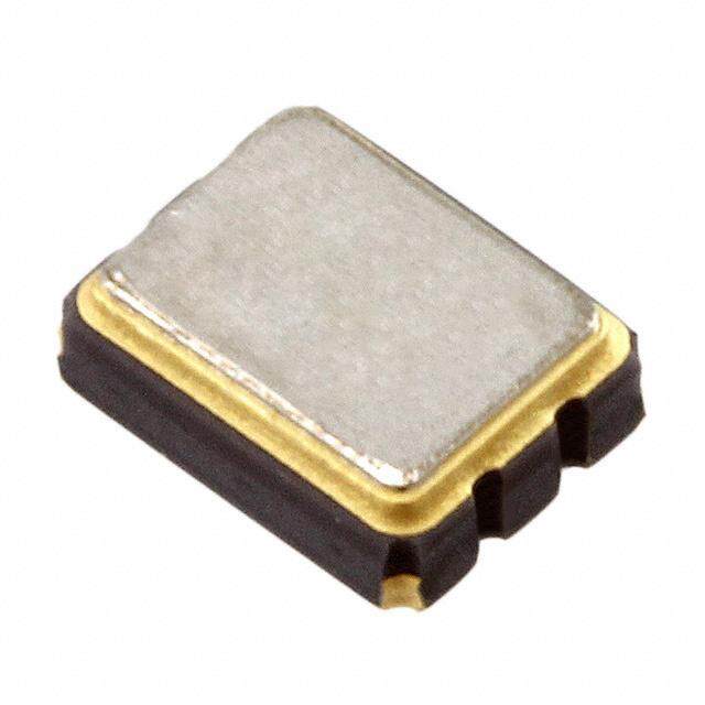
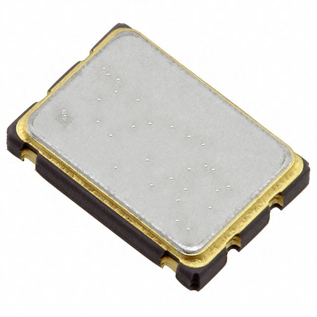
| 描述 | OSC XO 28.63636MHZ TTL PC PIN |
| 产品分类 | |
| 品牌 | EPSON |
| 数据手册 | |
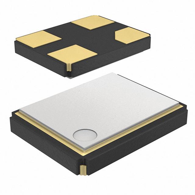
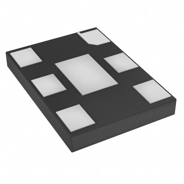
| 产品图片 |
|
| 产品型号 | SG-531PTJ 28.63636MC:ROHS |
| rohs | 无铅 / 符合限制有害物质指令(RoHS)规范要求 |
| 产品系列 | SG531 |
| 产品培训模块 | http://www.digikey.cn/PTM/IndividualPTM.page?site=cn&lang=zhs&ptm=25398 |
| 产品目录绘图 |
|
| 产品目录页面 | |
| 其它名称 | SER1820 |
| 功能 | 三态(输出启用) |
| 包装 | 管件 |
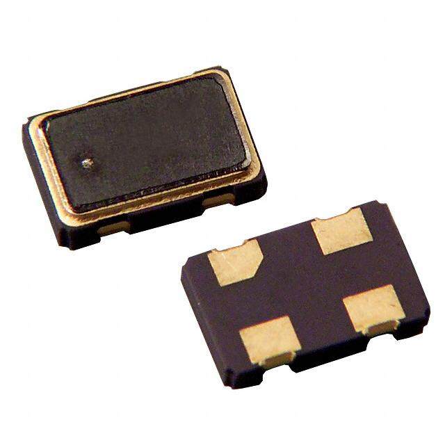
| 大小/尺寸 | 0.539" 长 x 0.260" 宽(13.70mm x 6.60mm) |
| 安装类型 | 通孔 |
| 封装/外壳 | 8-DIP,4 引线(半尺寸) |
| 工作温度 | -20°C ~ 70°C |
| 标准包装 | 35 |
| 电压-电源 | 5V |
| 电流-电源(最大值) | 35mA |
| 电流-电源(禁用)(最大值) | 28mA |
| 等级 | - |
| 类型 | XO(标准) |
| 输出 | TTL |
| 频率 | 28.63636MHz |
| 频率稳定度 | ±100ppm |
| 高度 | 0.209"(5.30mm) |


- 商务部:美国ITC正式对集成电路等产品启动337调查
- 曝三星4nm工艺存在良率问题 高通将骁龙8 Gen1或转产台积电
- 太阳诱电将投资9.5亿元在常州建新厂生产MLCC 预计2023年完工
- 英特尔发布欧洲新工厂建设计划 深化IDM 2.0 战略
- 台积电先进制程称霸业界 有大客户加持明年业绩稳了
- 达到5530亿美元!SIA预计今年全球半导体销售额将创下新高
- 英特尔拟将自动驾驶子公司Mobileye上市 估值或超500亿美元
- 三星加码芯片和SET,合并消费电子和移动部门,撤换高东真等 CEO
- 三星电子宣布重大人事变动 还合并消费电子和移动部门
- 海关总署:前11个月进口集成电路产品价值2.52万亿元 增长14.8%

PDF Datasheet 数据手册内容提取
Crystal oscillator Product Number (please contact us) SG-615 : Q33615xx2xxxx00 CRYSTAL OSCILLATOR (SPXO) SG -531 : Q32531xx2xxxx00 OUTPUT : CMOS, TTL SG -51 : Q32510xx2xxxx00 SG - 615 series SG - 531 SG - 51 series / Frequency range : 1.025 MHz to 135 MHz Supply voltage : 3.3 V Typ. / 5.0 V Typ. Actual size Function : Output enable(OE) or Standby(ST) SG-615 SG-531 SG-51 Pin compatible with full-size metal can. (SG-51 series) Pin compatible with half-size metal can. (SG-531 series) Specifications (characteristics) Specifications SG-615P SG-615PTJ Item Symbol Conditions / Remarks SG-531P SG-531PTJ SG-51P SG-51PTJ Output frequency range f0 1.025 MHz to 26 MHz 26.001 MHz to 66.667 MHz Please contact us about available frequencies. Supply voltage VCC 5.0 V 0.5 V Storage temperature T_stg -55 C to +125 C Storage as single product. Operating temperature T_use -20 C to +70 C Frequency tolerance f_tol B*1: 50 10-6, C: 100 10-6 -20 C to +70 C Current consumption ICC 23 mA Max. 35 mA Max. No load condition Disable current I_dis 12 mA Max. 28 mA Max. OE=GND Symmetry SYM 40 % to 60 % - CMOS load:50 % VCC level 40 % to 60 % 45 % to 55 % TTL load: 1.4 V level Output voltage VOH VCC-0.4 V Min. 2.4 V Min. IOH=-400 A VOL 0.4 V Max. IOL=16 mA(P)/ 8 mA(PTJ) Output load condition L_TTL 10 TTL Max. 5 TTL Max. L_CMOS 15 pF (TTL) Output load condition L_CMOS 50 pF Max. - (CMOS) VIH 2.0 V Min. 3.5 V Min. IIH= 1 A Max. (OE=VCC) Input voltage VIL 0.8 V Max. 1.5 V Max. PIILT=J -:I1IL0=0 -5A0 0M inA. M(OinE.=(OGEN=DG),N D ) Rise time / Fall time tr / tf 88 nnss MMaaxx.. 5 ns- M ax. CTTMLO loSa ldo:a0d.4:2 V0 t%o 2V.C4C V to le 8v0e l% VCC level Start-up time t_str 4 ms Max. 10 ms Max. Time at minimum supply voltage to be 0 s Frequency aging f_aging 5 10-6 / year Max. +25 C, VCC=5.0 V, First year *1 “B” tolerance will be available up to 55 MHz. Specifications (characteristics) Specifications Item Symbol SG-615PCG SG-615SCG Conditions / Remarks SG-615PCN SG-531PCG SG-531SCG 26.001 MHz Output frequency range f0 1.500 MHz to 26.000 MHz to 66.667 MHz Please contact us about available frequencies. Supply voltage VCC 2.7 V to 3.6 V 3.0 V to 3.6 V Storage temperature T_stg -55 C to +125 C Storage as single product. Operating temperature T_use -40 C to +85 C B: 50 10-6 C: 100 10-6 -20 C to +70 C Frequency tolerance f_tol M: 100 10-6 -40 C to +85 C Current consumption ICC 12 mA Max. 20 mA Max. No load condition Disable current I_dis 10 mA Max. - 10 mA Max. OE=GND (PCG,PCN) Stand-by current I_std - 50 A Max. - ST=GND (SCG) Symmetry SYM 45 % to 55 % 50 % VCC level, L_CMOS=Max. Output voltage VOH VCC-0.4 V Min. VCC-0.4 V Min. IOH=-8 mA VOL 0.4 V Max. 0.4 V Max. IOL= 8 mA Output load condition L_CMOS 25 pF Max. 15 pF Max. Input voltage VVIIHL 2700 %% VVCCCC MMainx.. 3700 %% VVCCCC MMainx.. OE Terminal orSTTerminal Rise time / Fall time tr / tf 4 ns Max. 20 % VCC to 80 % VCC level, L_CMOS Max. Start-up time t_str 12 ms Max. 10 ms Max. t=0 at 90% VCC Frequency aging f_aging 5 10-6 / year Max. +25 C, VCC=3.3 V, First year
Crystal oscillator Specifications (characteristics) Specifications Item Symbol SG-615PTW / STW SG-615PHW / SHW SG-615PCW / SCW Conditions / Remarks SG-531PTW / STW SG-531PHW / SHW SG-531PCW / SCW 26.001 MHz to Output frequency range f0 55.001 MHz to 135.000 MHz 135.000 MHz Please contact us about available frequencies. Supply voltage VCC 5.0 V 0.5 V 3.3 V 0.3 V Storage temperature T_stg -55 C to +125 C Storage as single product. Operating temperature T_use -20 C to +70 C -40 C to +85 C B: 50 10-6 , C*2: ±100 × 10-6 -20 C to +70 C Frequency tolerance f_tol - M: 100 10-6 -40 C to +85 C Current consumption ICC 45 mA Max. 28 mA Max. No load condition( Max. frequency range ) Disable current I_dis 30 mA Max. 16 mA Max. OE=GND (PTW,PHW,PCW) Stand-by current I_std 50 A Max. ST=GND (STW,SHW,SCW) Symmetry SYM - 40 % to 60 % 50 % VCC level, L_CMOS=Max. 40 % to 60 % - 1.4 V level ,L_CMOS=Max. Output voltage VOH VCC-0.4 V Min. IOH=-16 mA(PTW,STW,PHW,SHW),-8 mA(PCW,SCW) VOL 0.4 V Max. IOL= 16 mA(PTW,STW,PHW,SHW), 8 mA(PCW,SCW) Output load condition (TTL) L_TTL 5 TTL Max. - - f0 90 MHz , Max.supply voltage Output load condition L_CMOS 15 pF Max. Max.frequency , Max.supply voltage (CMOS) Input voltage VVIIHL 02..80 VV MMainx.. 2700 %% VVCCCC MMainx.. OE Terminal orSTTerminal Rise time / Fall time tr / tf 4 ns- M ax. - 4 ns Max. - 02.04 %V VtoC 2C .t4o V8 0le %ve lV CC level, L_CMOS Max. Start-up time t_str 10 ms Max.. Time at minimum supply voltage to be 0 s Frequency aging f_aging 5 10-6 / year Max. +25 C, VCC=5.0 V / 3.3 V, First year *2 “C” tolerance : f0 ≥66.667 MHz(PTW,STW,PHW,SHW) Product Name SG-615 P C G 20.000000MHz C ③Supply voltage ⑤Frequency tolerance (Standard form) ① ②③ ④ ⑤ C 3.3 V Typ. B ±50 × 10-6 / -20 to +70°C ①Model ②Function (P: Output enable, S:Standby) T,H 5.0 V Typ. C ±100 × 10-6 / -20 to +70°C ③Supply voltage ④Frequency Blank 5.0 V Typ. M ±100 × 10-6 / -40 to +85°C ⑤Frequency tolerance External dimensions (Unit:mm) Footprint(Recommended) (Unit:mm) . SG-615 series SG-615 series Pin map 1.3 14.0 Max. Pin Connection #4 #3 1 OE or ST SE2G0 - .609103505P02M AC 8.65 9.8 Max. 234 GOVNUCCDT 8 3.0 8. #1 #2 ax. 5 M 2 7 0. 0.51 4. 7.62 5.08 0.25Min. 5.08 SG-531 series Pin map SG-51 series #8 #5 No. Pin terminal #14 #8 Pin map Pin Connection 1 OE or ST #1 ES1 G36 .570 39.M013a0P5x0.T3 0BJ#4 6.6 458 GOVNUCCDT #1 ES1G1965..810 MP0a0 x90.3 M5H3#B7z 6.36 11784 OEGOV NUoCrCDT S T 7.62 x. 7.62 x. Ma 3 Ma 5.3 5. 0.25 n. 0.25 0.51 7.62 0.2Min. 54 Min. 90~105 0.51 15.24 0.2Min. 2.54 Mi 90~105 2. Note. OE pin (P,PTJ,PTW,PHW,PCW,PCN,PCG) ST pin (STW, SHW, SCW,SCG) OE pin = "H" or "open" : Specified frequency output. ST pin = "H" or "open" : Specified frequency output. OE pin = "L" : Output is high impedance. ST pin = "L" : Output is low level (weak pull - down),oscillation stops. To maintain stable operation, provide a 0.01uF to 0.1uF by-pass capacitor at a location as near as possible to the power source terminal of the crystal product (between Vcc - GND).
PROMOTION OF ENVIRONMENTAL MANAGEMENT SYSTEM CONFORMING TO INTERNATIONAL STANDARDS At Seiko Epson, all environmental initiatives operate under the Plan-Do-Check-Action (PDCA) cycle designed to achieve continuous ISO 14000 is an international standard for environmental improvements. The environmental management system (EMS) management that was established by the International operates under the ISO 14001 environmental management standard. Standards Organization in 1996 against the background of All of our major manufacturing and non-manufacturing sites, in growing concern regarding global warming, destruction of Japan and overseas, completed the acquisition of ISO 14001 the ozone layer, and global deforestation. certification. WORKING FOR HIGH QUALITY In order provide high quality and reliable products and services than meet customer needs, ISO/TS16949 is the international standard that added the Seiko Epson made early efforts towards obtaining ISO9000 series sector-specific supplemental requirements for automotive certification and has acquired ISO9001 for all business industry based on ISO9001. establishments in Japan and abroad. We have also acquired ISO/TS 16949 certification that is requested strongly by major automotive manufacturers as standard. ►Explanation of the mark that are using it for the catalog ►Pb free. ►Complies with EU RoHS directive. *About the products without the Pb-free mark. Contains Pb in products exempted by EU RoHS directive. (Contains Pb in sealing glass, high melting temperature type solder or other.) ►Designed for automotive applications such as Car Multimedia, Body Electronics, Remote Keyless Entry etc. ►Designed for automotive applications related to driving safety (Engine Control Unit, Air Bag, ESC etc ). Notice This material is subject to change without notice. Any part of this material may not be reproduced or duplicated in any form or any means without the written permission of Seiko Epson. The information about applied circuitry, software, usage, etc. written in this material is intended for reference only. Seiko Epson does not assume any liability for the occurrence of infringing on any patent or copyright of a third party. This material does not authorize the licensing for any patent or intellectual copyrights. When exporting the products or technology described in this material, you should comply with the applicable export control laws and regulations and follow the procedures required by such laws and regulations. You are requested not to use the products (and any technical information furnished, if any) for the development and/or manufacture of weapon of mass destruction or for other military purposes. You are also requested that you would not make the products available to any third party who may use the products for such prohibited purposes. These products are intended for general use in electronic equipment. When using them in specific applications that require extremely high reliability, such as the applications stated below, you must obtain permission from Seiko Epson in advance. / Space equipment (artificial satellites, rockets, etc.) / Transportation vehicles and related (automobiles, aircraft, trains, vessels, etc.) / Medical instruments to sustain life / Submarine transmitters / Power stations and related / Fire work equipment and security equipment / traffic control equipment / and others requiring equivalent reliability. All brands or product names mentioned herein are trademarks and/or registered trademarks of their respective. Seiko Epson Corporation