 Datasheet下载
- 型号: SESD0802Q4UG-0020-090
- 制造商: CORCOM/TYCO ELECTRONICS
- 库位|库存: xxxx|xxxx
- 要求:
| 数量阶梯 | 香港交货 | 国内含税 |
| +xxxx | $xxxx | ¥xxxx |
查看当月历史价格
查看今年历史价格
SESD0802Q4UG-0020-090产品简介:
ICGOO电子元器件商城为您提供SESD0802Q4UG-0020-090由CORCOM/TYCO ELECTRONICS设计生产,在icgoo商城现货销售,并且可以通过原厂、代理商等渠道进行代购。 SESD0802Q4UG-0020-090价格参考¥2.68-¥7.38。CORCOM/TYCO ELECTRONICSSESD0802Q4UG-0020-090封装/规格:TVS - 二极管, 9.2V (Typ) Clamp 2A (8/20µs) Ipp Tvs Diode Surface Mount 0802。您可以下载SESD0802Q4UG-0020-090参考资料、Datasheet数据手册功能说明书,资料中有SESD0802Q4UG-0020-090 详细功能的应用电路图电压和使用方法及教程。
Littelfuse Inc. 的 SESD0802Q4UG-0020-090 是一款瞬态电压抑制(TVS)二极管,属于表面贴装型静电保护器件,专为高速数据线路和敏感电子元件提供可靠的ESD(静电放电)防护。该器件具有低电容特性,适用于需要保持信号完整性的高速接口。

其主要应用场景包括:

1. 消费类电子产品:广泛用于智能手机、平板电脑和笔记本电脑中的USB端口(如USB 2.0/3.0)、HDMI接口、音频插孔等,防止人体静电或操作过程中产生的瞬态电压损坏内部电路。

2. 通信设备:应用于路由器、交换机、光模块等设备的数据线保护,确保信号传输稳定并提升系统可靠性。

3. 工业控制系统:用于保护PLC、传感器接口、人机界面(HMI)等关键控制节点,抵御工业环境中可能存在的静电干扰和电气瞬变。

4. 汽车电子:适合车载信息娱乐系统、USB充电端口及CAN总线等低压信号线路的ESD防护,满足车规级电磁兼容性要求。

SESD0802Q4UG-0020-090 具有快速响应时间、低钳位电压和高可靠性,符合IEC 61000-4-2 Level 4(±8kV接触放电)等国际标准,是高性能ESD保护的理想选择。其小型化封装(如DFN)节省PCB空间,适用于高密度布局设计。
| 参数 | 数值 |
| 品牌 | TE Connectivity / Raychem |
| 产品目录 | |
| 描述 | ESD 抑制器 4-CH MINI 9V Uni-Di .20pF 20kV SESD |
| 产品分类 | ESD 抑制器 |
| 产品手册 | |
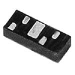
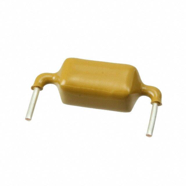
| 产品图片 |
|
| rohs | 符合RoHS |
| 产品系列 | TE Connectivity / Raychem SESD0802Q4UG-0020-090 |
| mouser_ship_limit | 该产品可能需要其他文件才能进口到中国。 |
| 产品型号 | SESD0802Q4UG-0020-090 |
| 产品种类 | ESD 抑制器 |
| 击穿电压 | 9 V |
| 商标 | TE Connectivity / Raychem |
| 封装 | Reel |
| 封装/箱体 | 0802 |
| 工作温度范围 | - 55 C to + 125 C |
| 工作电压 | 9 V |
| 工厂包装数量 | 5000 |
| 电容 | 0.2 pF |
| 端接类型 | SMD/SMT |
| 系列 | SESD |
| 通道 | 4 Channels |
| 钳位电压 | 9.18 V |
| 零件号别名 | RF3076-000 |


- 商务部:美国ITC正式对集成电路等产品启动337调查
- 曝三星4nm工艺存在良率问题 高通将骁龙8 Gen1或转产台积电
- 太阳诱电将投资9.5亿元在常州建新厂生产MLCC 预计2023年完工
- 英特尔发布欧洲新工厂建设计划 深化IDM 2.0 战略
- 台积电先进制程称霸业界 有大客户加持明年业绩稳了
- 达到5530亿美元!SIA预计今年全球半导体销售额将创下新高
- 英特尔拟将自动驾驶子公司Mobileye上市 估值或超500亿美元
- 三星加码芯片和SET,合并消费电子和移动部门,撤换高东真等 CEO
- 三星电子宣布重大人事变动 还合并消费电子和移动部门
- 海关总署:前11个月进口集成电路产品价值2.52万亿元 增长14.8%


PDF Datasheet 数据手册内容提取
TVS Diode Arrays (SPA ® Diodes) SESD Series Ultra Low Capacitance Diode Arrays SESD Series Ultra Low Capacitance Diode Arrays RoHS Pb GREEN ELV Description The SESD series Ultra Low Capacitance Diode Arrays provides signal integrity-preserving unidirectional ESD protection for the world’s most challenging high speed serial interfaces. Compelling packaging options including the standard 1004 DFN 2.5 mm x 1.0 mm layout, the board space-friendly 0802 DFN and 1103 DFN minimize trace layout complexity, and save significant PCB space. The 0402 DFN provides the most flexibility for PCB layout purposes. This series is rated in excess of 20kV contact ESD protection (IEC 61000-4-2) while maintaining extremely low leakage and dynamic resistance, and is offered in the industry’s most progressive and popular footprints. The SESD series sets higher standards for signal Pinout integrity and usability. 0402 DFN array 0802 DFN array Features 1 2 4 3 • 0.20pF TYP capacitance • AEC-Q101 qualified • ESD, IEC 61000-4-2, • Moisture Sensitivity ±20kV contact, ±20kV air Level(MSL-1) 1 G 2 • Low clamping voltage • ELV Compliant 3 of 9.2V @ I =2.0A • RoHS Compliant and PP (t =8/20μs) Lead Free P • Low profile DFN array • PPAP capable 1004 DFN array 1103 DFN array packages 1 2 3.G 4 5 3 2 G 1 • Facilitates excellent signal integrity 10 9 8.G 7 6 4 5 6 Applications • USB 3.1, 3.0, 2.0 • Tablet PC and external Bottom View • HDMI 2.0, 1.4a, 1.3 storage with high speed interfaces • DisplayPort(TM) • Applications requiring • V-by-One®) high ESD performance in Functional Block Diagram • Thunderbolt small packages 1 2 4 5 1 2 • LVDS interfaces • Automotive applications • Consumer, mobile and portable electronics Additional Information G, 3, 8 3 0802/1004 DFN array 0402 DFN array Datasheet Resources Samples 1 2 3 4 5 6 G 1103 DFN array © 2019 Littelfuse, Inc. Specifications are subject to change without notice. Revised: 09/09/19
TVS Diode Arrays (SPA ® Diodes) SESD Series Ultra Low Capacitance Diode Arrays Absolute Maximum Ratings Symbol Parameter Value Units I Peak Current (t=8/20μs) 2.0 A PP p T Operating Temperature -55 to 125 °C OP T Storage Temperature -55 to 150 °C STOR CAUTION: Stresses above those listed in “Absolute Maximum Ratings” may cause permanent damage to the component. This is a stress only rating and operation of the component at these or any other conditions above those indicated in the operational sections of this specification is not implied. Electrical Characteristics - (T =25°C) OP Parameter Test Conditions Min Typ Max Units Input Capacitance @ V = 0V, f = 3GHz 0.20 0.22 pF R Breakdown Voltage V @ I=1mA 9.00 V BR T Reverse Working Voltage 7.0 V Reverse Leakage Current I @ V =5.0V 25 50 nA L RWM Clamping Voltage V @ I =2.0A 9.20 V CL PP Peak Pulse Current t=8/20μs 2.0 A P IEC61000-4-2 (Contact) ±20 ESD Withstand Voltage kV IEC 61000-4-2 (Air) ±20 Insertion Loss Diagram Insertion Loss Diagram - 1103 DFN Array 0 0 -5.0 -5.0 oss (dB) -10.0 ss (dB) -10.0 L o on -15.0 n L -15.0 21 Inserti -20.0 1 Insertio -20.0 S -25.0 S2 -25.0 -30.0 -30.0 1.E+06 1.E+07 1.E+08 1.E+09 1.E+10 1.E+06 1.E+07 1.E+08 1.E+09 1.E+10 Frequency (Hz) Frequency (Hz) © 2019 Littelfuse, Inc. Specifications are subject to change without notice. Revised: 09/09/19
TVS Diode Arrays (SPA ® Diodes) SESD Series Ultra Low Capacitance Diode Arrays Component IV Curve 1.0 0.8 0.6 0.4 0.2 )Am 0.0 ( tn -0.2 erruC -0.4 -0.6 -0.8 -1.0 -2 -1 0 1 2 3 4 5 6 7 8 9 10 Voltage (V) USB3.0 Eye Diagram 5.0 Gb/s, 1000mV differential, CPO Compliant Test Pattern Without SESD Device With SESD Device Soldering Parameters Reflow Condition Pb – Free assembly t P T - Temperature Min (T ) 150°C P CCrriittiiccaall ZZoonnee s(min) RRaammpp--uupp TTLL ttoo TTPP Pre Heat - Temperature Max (T ) 200°C - Time (min to max) (tss(m)ax) 60 – 180 secs eruta TS(maTx)L tL Average ramp up rate (Liquidus) Temp (TL) to peak 3°C/second max rep RRaammpp--ddoowwn TS(max) to TL - Ramp-up Rate 3°C/second max meT T PPrreehheeaatt - Temperature (T) (Liquidus) 217°C S(min) Reflow L tS - Temperature (t) 60 – 150 seconds L Peak Temperature (T) 260+0/-5 °C 25 Time within 5°C of aPctual peak Temperature (t) 20 – 40 seconds time to peak temperature Time p Ramp-down Rate 6°C/second max Time 25°C to peak Temperature (T) 8 minutes Max. P Do not exceed 260°C © 2019 Littelfuse, Inc. Specifications are subject to change without notice. Revised: 09/09/19
TVS Diode Arrays (SPA ® Diodes) SESD Series Ultra Low Capacitance Diode Arrays Package Dimensions — 0402 DFN Array Millimeters Inches Symbol Min Typ Max Min Typ Max A 0.33 0.38 0.43 0.013 0.015 0.017 A1 0 - 0.05 0 - 0.002 A3 0.13 ref. 0.005 ref. D 0.55 0.60 0.65 0.022 0.024 0.026 E 0.95 1.00 1.05 0.037 0.039 0.041 K 0.35 0.40 0.45 0.014 0.016 0.018 L1 0.45 0.50 0.55 0.018 0.020 0.022 L2 0.20 0.25 0.30 0.008 0.010 0.012 b 0.10 0.15 0.20 0.004 0.006 0.008 e1 0.35 BSC 0.014 BSC e2 0.65 BSC 0.026 BSC Symbol Millimeters Inches A 0.60 0.024 B 1.00 0.039 C 0.23 0.009 D 0.35 0.014 D1 0.35 0.014 E 0.15 0.006 F 0.30 0.012 Pad Layout Embossed Carrier Tape & Reel Specification — 0402 DFN Array T D0 P2 P0 Y E1 Symbol Millimeters A0 0.70+/-0.05 D1 B0 1.15+/-0.05 F W D0 ø 1.55 + 0.05 B0 D1 ø 0.40 +/- 0.05 E1 1.75+/-0.10 K0 F 3.50+/-0.05 A0 K0 0.47+/-0.05 Section Y - Y Y P1 P0 4.00+/-0.10 P1 2.00+/-0.05 User Feeding Direction P2 2.00+/-0.05 W 8.00 +/-0.10 T 0.20+/-0.05 Pin 1 Location © 2019 Littelfuse, Inc. Specifications are subject to change without notice. Revised: 09/09/19
TVS Diode Arrays (SPA ® Diodes) SESD Series Ultra Low Capacitance Diode Arrays Package Dimensions — 0802 DFN Array Millimeters Inches Symbol Min Typ Max Min Typ Max A 0.33 0.38 0.43 0.013 0.015 0.017 A1 0 0.02 0.05 0 -- 0.002 A3 0.127 ref 0.005 ref. D 0.50 0.60 0.70 0.020 0.024 0.028 E 1.90 2.00 2.10 0.075 0.079 0.083 b 0.15 0.20 0.25 0.006 0.008 0.010 b1 0.25 0.30 0.36 0.010 0.012 0.014 L 0.25 0.30 0.36 0.010 0.012 0.014 L1 0.35 0.40 0.45 0.014 0.016 0.018 L2 0.05 BSC 0.002 BSC e 0.40 BSC 0.016 BSC e1 0.45 BSC 0.018 BSC e2 0.25 BSC 0.010 BSC N 4 4 Symbol Millimeters Inches A 0.60 0.024 B 2.00 0.079 C 0.30 0.012 D 0.30 0.012 E 0.25 0.010 F 0.10 0.004 F1 0.15 0.006 G 0.40 BSC 0.016 BSC G1 0.45 BSC 0.018 BSC Pad Layout Embossed Carrier Tape & Reel Specification — 0802 DFN Array T D0 P2 P0 Y E1 Symbol Millimeters A0 0.81+/-0.05 D1 B0 2.21+/-0.05 F W D0 ø 1.50+0.10/-0 B0 D1 ø 0.40 min E1 1.75+/-0.10 F 3.50+/-0.05 K0 K0 0.46+/-0.05 A0 Section Y - Y Y P1 P0 4.00+/-0.10 P1 2.00+/-0.10 User Feeding Direction P2 2.00+/-0.05 W 8.00+0.30/-0.10 T 0.25+/-0.20 Pin 1 Location © 2019 Littelfuse, Inc. Specifications are subject to change without notice. Revised: 09/09/19
TVS Diode Arrays (SPA ® Diodes) SESD Series Ultra Low Capacitance Diode Arrays A1 D 8xb LxN Package Dimensions — 1004 DFN Array D A1 8xb5 LxN 6 Symbol Millimeters Inches Min Typ Max Min Typ Max 4 7 L1 2x5 6 A 0.33 0.38 0.43 0.013 0.015 0.017 E 3 R1 8b1 2x A1 0.00 0.02 0.05 0 -- 0.002 L1e 21x4Gnd 7Gnd A D3 0.90 0.1 12.070 r e f. 1.10 0.035 0. 000.053 r9e f. 0.043 E e1e Gnd32 R1 2xR Gnd89b1 2x E 2.40 2.50 2.60 0.094 0.098 0.102 b 0.15 0.20 0.25 0.006 0.008 0.010 21 9N=10 b1 0.35 0.40 0.45 0.014 0.016 0.018 e 2xR A3 1 =10 L 0.33 0.38 0.43 0.013 0.015 0.017 A N L1 0.00 0.10 0.15 0.000 0.004 0.006 A3 e 0.50 BSC 0.020 BSC A e1 0.50 BSC 0.020 BSC SIDE VIEW 1 TOP VIEW SIDE VIEW 2 BOTTOM VIEW R 0.08 BSC 0.003 BSC (Front) SIDE VIEW 1 TOP VIEW SIDE VIEW 2 BOTTOM VIEW R1 0.13 BSC 0.005 BSC (Front) N 10 10 END VIEW 1 END VIEW 2 END VIEW 1 END VIEW 2 Symbol Millimeters Inches A 1.20 0.047 AA 2x2 Fx 2Fx2 xF 1F1 AA 2x2 Fx 2Fx2 Fx1 F1 BC 20..2500 00..008270 2x D21x D1 D 0.20 0.008 D1 0.40 0.016 B B 4x G GG41x41 xG G BB DD11 G1 EF 00..3200 00..001028 4x G 4x4 Gx G G1 F1 0.20 0.008 8x D G 0.50 BSC 0.020 BSC 8x D E 88xx DD E G1 1.00 BSC 0.039 BSC E 8x C 8x C E 8x CRecommended 8x C Alternate Recommended Alternate Pad Layout Pad Layout Embossed Carrier Tape & Reel Specification — 1004 DFN Array T D0 P2 P0 Y E1 Symbol Millimeters A0 1.20+/-0.05 D1 B0 2.70+/-0.05 F W D0 ø 1.50+0.10/-0 B0 D1 ø 0.50 min E1 1.75+/-0.10 K0 F 3.50+/-0.05 A0 K0 0.51+/-0.10 Section Y - Y Y P1 P0 4.00+/-0.10 P1 4.00+/-0.10 P2 2.00+/-0.05 W 8.00+0.30/-0.10 T 0.25+/-0.05 © 2019 Littelfuse, Inc. Specifications are subject to change without notice. Revised: 09/09/19
TVS Diode Arrays (SPA ® Diodes) SESD Series Ultra Low Capacitance Diode Arrays Package Dimensions — 1103 DFN Array Millimeters Inches Symbol Min Typ Max Min Typ Max A 0.33 0.38 0.43 0.013 0.015 0.017 A1 0.00 0.02 0.05 0 -- 0.002 A3 0.127 ref. 0.005 ref. D 0.70 0.80 0.90 0.027 0.031 0.035 E 2.70 2.80 2.90 0.106 0.110 0.114 b 0.15 0.20 0.25 0.006 0.008 0.010 b1 0.25 0.30 0.35 0.010 0.012 0.014 L 0.30 0.35 0.40 0.012 0.014 0.016 L1 0.50 0.55 0.60 0.019 0.021 0.024 L2 0.05 BSC 0.002 BSC e 0.40 BSC 0.016 BSC e1 0.45 BSC 0.018 BSC e2 0.40 BSC 0.016 BSC N 6 6 Symbol Millimeters Inches A 0.80 0.031 B 2.80 0.110 C 0.35 0.014 D 0.30 0.012 E 0.45 0.018 F 0.10 0.004 F1 0.15 0.006 G 0.40 BSC 0.016 BSC G1 0.45 BSC 0.018 BSC Pad Layout Embossed Carrier Tape & Reel Specification — 1103 DFN Array Symbol Millimeters T D0 P2 P0 Y E1 A0 1.00+/-0.05 B0 3.00+/-0.05 D1 D0 ø 1.50+0.10/-0 F D1 ø 0.50 min W B0 E1 1.75+/-0.10 F 3.50+/-0.05 K0 0.51+/-0.05 K0 P0 4.00+/-0.10 A0 Section Y - Y Y P1 P1 4.00+/-0.10 P2 2.00+/-0.05 W 8.00+0.30/-0.10 T 0.25+/-0.05 © 2019 Littelfuse, Inc. Specifications are subject to change without notice. Revised: 09/09/19
TVS Diode Arrays (SPA ® Diodes) SESD Series Ultra Low Capacitance Diode Arrays Part Numbering System Part Marking System SESD xxxx Q xUG0020–090 Breakdown Voltage SESD product 090: 9.0V (TYP) C MC Package Input Capacitance 0402 0020: 0.20pF (TYP) 0802 1004 Common GND pin 0402 0802 1103 Directional DFN Array Package U: Unidirectional 4C 6C No of channel 2: Two Channels 4: Four Channels 6: Six Channels 1004 1103 Ordering Information Part Number Package Ordering Part Number Minimum Order Quantity SESD0402Q2UG-0020-090 0402 DFN Array RF2946-000 50,000 SESD0802Q4UG-0020-090 0802 DFN Array RF3076-000 25,000 SESD1004Q4UG-0020-090 1004 DFN Array RF3077-000 25,000 SESD1103Q6UG-0020-090 1103 DFN Array RF3078-000 25,000 Disclaimer Notice - Information furnished is believed to be accurate and reliable. However, users should independently evaluate the suitability of and test each product selected for their own applications. Littelfuse products are not designed for, and may not be used in, all applications. Read complete Disclaimer Notice at http://www.littelfuse.com/disclaimer-electronics. © 2019 Littelfuse, Inc. Specifications are subject to change without notice. Revised: 09/09/19