 Datasheet下载
- 型号: SESD0402X1UN-0020-090
- 制造商: CORCOM/TYCO ELECTRONICS
- 库位|库存: xxxx|xxxx
- 要求:
| 数量阶梯 | 香港交货 | 国内含税 |
| +xxxx | $xxxx | ¥xxxx |
查看当月历史价格
查看今年历史价格
SESD0402X1UN-0020-090产品简介:
ICGOO电子元器件商城为您提供SESD0402X1UN-0020-090由CORCOM/TYCO ELECTRONICS设计生产,在icgoo商城现货销售,并且可以通过原厂、代理商等渠道进行代购。 SESD0402X1UN-0020-090价格参考¥0.95-¥0.95。CORCOM/TYCO ELECTRONICSSESD0402X1UN-0020-090封装/规格:TVS - 二极管, 。您可以下载SESD0402X1UN-0020-090参考资料、Datasheet数据手册功能说明书,资料中有SESD0402X1UN-0020-090 详细功能的应用电路图电压和使用方法及教程。
Littelfuse Inc. 的型号 SESD0402X1UN-0020-090 是一款 TVS(瞬态电压抑制器)二极管,主要用于保护电子设备免受过电压事件(如静电放电 ESD、雷击浪涌和开关瞬变)的影响。以下是该型号的一些典型应用场景:

 1. 消费类电子产品
   - 智能手机和平板电脑:用于保护USB接口、耳机插孔、摄像头模块等敏感电路,防止ESD损害。
   - 电视和显示器:保护HDMI、VGA和其他输入/输出端口,避免信号传输过程中可能出现的电压瞬变。
   - 音频设备:保护音频输入/输出端口,确保音质不受干扰。

 2. 通信设备
   - 网络路由器和交换机:保护以太网端口、Wi-Fi模块和其他通信接口,增强设备的可靠性。
   - 光纤收发器:在高速数据传输中提供ESD保护,确保信号完整性。
   - 基站和无线模块:防止雷击或高压瞬变对射频前端电路的破坏。

 3. 汽车电子
   - 车载信息娱乐系统:保护触摸屏、导航系统和蓝牙模块等组件。
   - 传感器和控制系统:为倒车雷达、摄像头和其他传感器提供可靠的过压保护。
   - CAN/LIN总线接口:防止电磁干扰和瞬态电压对通信线路的影响。

 4. 工业自动化
   - 可编程逻辑控制器 (PLC):保护输入/输出端口,确保工业控制系统的稳定运行。
   - 人机界面 (HMI):保护触摸屏和通信接口,提升用户体验。
   - 工业传感器:防止恶劣环境中的瞬态电压对精密测量设备的影响。

 5. 医疗设备
   - 便携式医疗设备:如血糖仪、血压计等,保护其USB接口和传感器。
   - 监护仪和诊断设备:防止ESD或浪涌对患者数据采集和显示模块的影响。

 6. 物联网 (IoT) 设备
   - 智能家居设备:如智能灯泡、插座和安防摄像头,保护其无线模块和电源接口。
   - 传感器节点:为温湿度传感器、烟雾报警器等提供可靠保护。

 特性总结
SESD0402X1UN-0020-090 具有小尺寸(适合紧凑设计)、低电容(减少信号失真)和高响应速度的特点,非常适合需要快速抑制瞬态电压的应用场景。它能够有效降低因过压导致的设备故障率,延长产品寿命,并提高整体系统的可靠性。
| 参数 | 数值 |
| 产品目录 | |
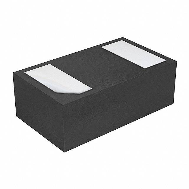
| 描述 | TVS DIODE 7VWM 9.2VC SMDESD 抑制器 1-CH 0402 9V Uni-Di .20pF 20kV SESD |
| 产品分类 | |
| 品牌 | TE Connectivity |
| 产品手册 | |
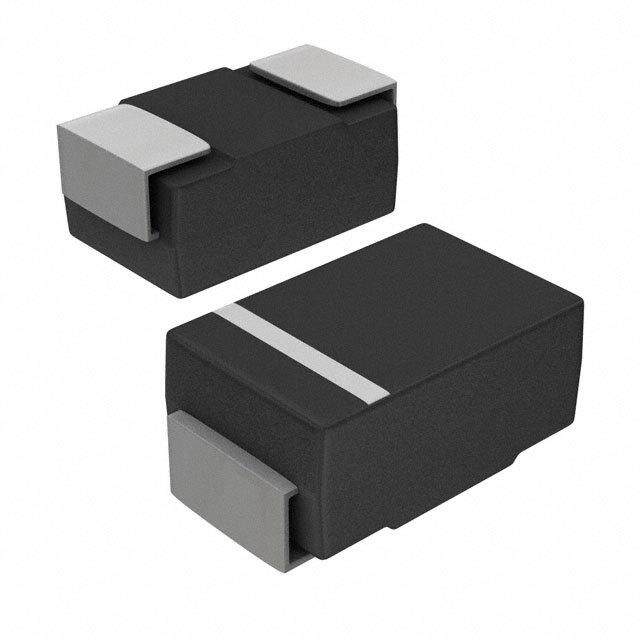
| 产品图片 |
|
| rohs | 符合RoHS无铅 / 符合限制有害物质指令(RoHS)规范要求 |
| 产品系列 | TE Connectivity / Raychem SESD0402X1UN-0020-090Raychem |
| mouser_ship_limit | 该产品可能需要其他文件才能进口到中国。 |
| 数据手册 | http://www.te.com/commerce/DocumentDelivery/DDEController?Action=srchrtrv&DocNm=SCD28186&DocType=SS&DocLang=ENhttp://www.te.com/commerce/DocumentDelivery/DDEController?Action=srchrtrv&DocNm=DS28296&DocType=DS&DocLang=English |
| 产品型号 | SESD0402X1UN-0020-090 |
| 不同频率时的电容 | 0.2pF @ 3MHz |
| 产品种类 | ESD 抑制器 |
| 供应商器件封装 | 2-XDFN(0.60x1) |
| 其它名称 | RF2194-000CT |
| 击穿电压 | 9 V |
| 功率-峰值脉冲 | - |
| 包装 | 剪切带 (CT) |
| 单向通道 | 1 |
| 双向通道 | - |
| 商标 | TE Connectivity / Raychem |
| 安装类型 | 表面贴装 |
| 封装 | Reel |
| 封装/外壳 | 2-XDFN |
| 封装/箱体 | 0402 (1005 metric) |
| 工作温度 | -55°C ~ 125°C (TJ) |
| 工作温度范围 | - 55 C to + 125 C |
| 工作电压 | 9 V |
| 工厂包装数量 | 10000 |
| 应用 | 通用 |
| 标准包装 | 1 |
| 电压-击穿(最小值) | 9V (标准) |
| 电压-反向关态(典型值) | 7V (最小值) |
| 电压-箝位(最大值)@Ipp | 9.2V (标准) |
| 电容 | 0.2 pF |
| 电流-峰值脉冲(10/1000µs) | 2A (8/20µs) |
| 电源线路保护 | 无 |
| 端接类型 | SMD/SMT |
| 类型 | 齐纳 |
| 系列 | SESD |
| 视频文件 | http://www.digikey.cn/classic/video.aspx?PlayerID=1364138032001&width=640&height=455&videoID=1571319073001 |
| 通道 | 1 Channel |
| 钳位电压 | 9.18 V |
| 零件号别名 | RF2194-000 |


- 商务部:美国ITC正式对集成电路等产品启动337调查
- 曝三星4nm工艺存在良率问题 高通将骁龙8 Gen1或转产台积电
- 太阳诱电将投资9.5亿元在常州建新厂生产MLCC 预计2023年完工
- 英特尔发布欧洲新工厂建设计划 深化IDM 2.0 战略
- 台积电先进制程称霸业界 有大客户加持明年业绩稳了
- 达到5530亿美元!SIA预计今年全球半导体销售额将创下新高
- 英特尔拟将自动驾驶子公司Mobileye上市 估值或超500亿美元
- 三星加码芯片和SET,合并消费电子和移动部门,撤换高东真等 CEO
- 三星电子宣布重大人事变动 还合并消费电子和移动部门
- 海关总署:前11个月进口集成电路产品价值2.52万亿元 增长14.8%


PDF Datasheet 数据手册内容提取
TVS Diode Arrays (SPA ® Diodes) SESD Series Enhanced ESD Diode Arrays SESD Series Ultra Low Capacitance Discrete TVS RoHS Pb GREEN ELV Description The SESD Series Ultra Low Capacitance Discrete TVS provides unidirectional and bidirectional ESD protection for the world’s most challenging high speed serial interfaces. Ultra low capacitance permits excellent signal integrity on the most challenging consumer electronics interfaces, such as USB 3.1, HDMI 2.0, DisplayPort, and V-by-One®. Providing in excess of 20kV contact ESD protection (IEC61000-4-2) while maintaining extremely low leakage and dynamic resistance, offered in the industry’s most popular footprints (0402 and 0201), the SESD series sets higher standards for signal integrity and usability. Pinout Features • 0.13pF MAX bidirectional • Low profile 0201 and 0402 DFN • 0.25pF MAX unidirectional 0402 DFN packages 0201DFN • ESD, IEC61000-4-2, • Facilitates excellent signal 1 integrity 1 ±20kV contact, ±20kV air • AEC-Q101 qualified • Low clamping voltage of 10V @ I =2A • ELV Compliant PP (Bidirectional) (t =8/20μs) P 2 2 Applications Bottom View • Ultra-high speed data • Consumer, mobile and lines portable electronics Functional Block Diagram • USB 3.1, 3.0, 2.0 • Tablet PC and external • HDMI 2.0, 1.4a, 1.3 storage with high speed interfaces 1 • DisplayPort(TM) 1 • Applications requiring • Thunderbolt (Light Peak) high ESD performance in • V-by-One® small packages • LVDS interfaces 2 2 Unidirectional Bidirectional © 2015 Littelfuse, Inc. Specifications are subject to change without notice. Revised: 05/26/15
TVS Diode Arrays (SPA ® Diodes) SESD Series Enhanced ESD Diode Arrays Absolute Maximum Ratings Thermal Information Symbol Parameter Value Units Parameter Rating Units I Peak Current (t=8/20μs) 2.0 A Storage Temperature Range -55 to 150 °C PP p T Operating Temperature -55 to 125 °C Maximum Junction Temperature 150 °C OP Maximum Lead Temperature T Storage Temperature -55 to 150 °C 260 °C STOR (Soldering 20-40s) CAUTION: Stresses above those listed in “Absolute Maximum Ratings” may cause permanent damage to the device. This is a stress only rating and operation of the device at these or any other conditions above those indicated in the operational sections of this specification is not implied. Unidirectional Electrical Characteristics - (T =25°C) OP Parameter Test Conditions Min Typ Max Units Input Capacitance @ V = 0V, f = 3GHz 0.20 0.25 pF R Breakdown Voltage V @ I=1mA 9.00 V BR T Reverse Working Voltage 7.0 V Reverse Leakage Current I @ V =5.0V 25 50 nA L RWM Clamping Voltage V @ I =2.0A 9.20 V CL PP IEC61000-4-2 (Contact) ±20 ESD Withstand Voltage kV IEC61000-4-2 (Air) ±20 Bidirectional Electrical Characteristics - (T =25°C) OP Parameter Test Conditions Min Typ Max Units Input Capacitance @ V = 0V, f = 3GHz 0.10 0.13 pF R Breakdown Voltage V @ I=1mA 9.80 V BR T Reverse Working Voltage -7.0 7.0 V Reverse Leakage Current I @ V =5.0V 25 50 nA L RWM Clamping Voltage V @ I =2.0A 10.0 V CL PP IEC61000-4-2 (Contact) ±20 ESD Withstand Voltage kV IEC61000-4-2 (Air) ±20 Insertion Loss Diagram - Unidirectional Insertion Loss Diagram - Bidirectional 0 0 -5.0 -5.0 S21 Insertion Loss (dB) ----12120505....0000 S21 Insertion Loss (dB) ----12120505....0000 -30.0 -30.0 1.E+06 1.E+07 1.E+08 1.E+09 1.E+10 1.E+06 1.E+07 1.E+08 1.E+09 1.E+10 Frequency (Hz) Frequency (Hz) © 2015 Littelfuse, Inc. Specifications are subject to change without notice. Revised: 05/26/15
TVS Diode Arrays (SPA ® Diodes) SESD Series Enhanced ESD Diode Arrays Device IV Curve - Unidirectional Device IV Curve - Bidirectional 1.0 1.0 0.8 0.8 0.6 0.6 0.4 0.4 0.2 0.2 )Am 0.0 )Am 0.0 ( tnerruC --00..24 ( tnerruC --00..24 -0.6 -0.6 -0.8 -0.8 -1.0 -1.0 -2 -1 0 1 2 3 4 5 6 7 8 9 10 -10 -8 -6 -4 -2 0 2 4 6 8 10 Voltage (V) Voltage (V) USB3.0 Eye Diagram 5.0 Gb/s, 1000mV differential, CPO Compliant Test Pattern Without SESD Device With SESD Device Soldering Parameters Reflow Condition Pb – Free assembly tP - Temperature Min (T ) 150°C TP CCrriittiiccaall ZZoonnee Pre Heat - Temperature Max (Ts(min)) 200°C e RRaammpp--uupp TTLL ttoo TTPP - Time (min to max) (tss()max) 60 – 180 secs rutare TS(mTaxL) tL Average ramp up rate (Liquidus) Temp (TL) 3°C/second max pm RRaammpp--ddoown to peak eT PPrreehheeaatt TS(min) TS(max) to TL - Ramp-up Rate 3°C/second max tS - Temperature (T) (Liquidus) 217°C Reflow L 25 - Temperature (tL) 60 – 150 seconds time to peak temperature Time Peak Temperature (T) 260+0/-5 °C P Time within 5°C of actual peak 20 – 40 seconds Product Characteristics of 0402 DFN Package Temperature (t) p Ramp-down Rate 6°C/second max Lead Plating Pre-Plated Frame Time 25°C to peak Temperature (T) 8 minutes Max. Lead Material Copper Alloy P Do not exceed 260°C Lead Coplanarity 0.0004 inches (0.102mm) Substrate material Silicon Body Material Molded Epoxy Flammability UL 94 V-0 Notes : 1. All dimensions are in millimeters 2. Dimensions include solder plating. 3. Dimensions are exclusive of mold flash & metal burr. 4. Blo is facing up for mold and facing down for trim/form, i.e. reverse trim/form. 5. Package surface matte finish VDI 11-13. © 2015 Littelfuse, Inc. Specifications are subject to change without notice. Revised: 05/26/15
TVS Diode Arrays (SPA ® Diodes) SESD Series Enhanced ESD Diode Arrays Package Dimensions — 0201 DFN Millimeters Inches A3 Symbol Min Typ Max Min Typ Max A 0.28 0.30 0.32 0.011 0.012 0.013 END VIEW A1 0 - 0.05 0 - 0.002 D b A3 0.102 ref. 0.004 ref. 2 D 0.25 0.30 0.35 0.010 0.012 0.014 L1 E 0.55 0.60 0.65 0.022 0.024 0.026 E K e PCI0N.0 15 ID K 0.11 0.17 0.22 0.004 0.007 0.009 L2 1 b 0.20 0.25 0.30 0.008 0.010 0.012 L1 0.13 0.18 0.23 0.005 0.008 0.009 SIDE VIEW 1 TOP VIEW SIDE VIEW 2 BOTTOM VIEW L2 0.14 0.19 0.24 0.006 0.007 0.009 e 0.356 BSC 0.014 BSC A M 0.32 0.013 A1 N 0.24 0.009 END VIEW O 0.62 0.024 P 0.14 0.006 M P O N Package Dimensions — 0402 DFN A3 Millimeters Inches Symbol Min Typ Max Min Typ Max END VIEW A 0.33 0.38 0.43 0.013 0.015 0.017 A1 0 - 0.05 0 - 0.002 D b A3 0.13 ref. 0.005 ref. L D 0.55 0.60 0.65 0.022 0.024 0.026 E K e E 0.95 1.00 1.05 0.037 0.039 0.041 K 0.35 0.40 0.45 0.014 0.016 0.018 PIN 1 ID b 0.45 0.50 0.55 0.018 0.020 0.022 0.125 x 45° SIDE VIEW1 TOP VIEW SIDE VIEW2 BOTTOM VIEW L 0.20 0.25 0.30 0.008 0.010 0.012 e 0.65 BSC 0.026 BSC M 0.60 0.024 A N 0.35 0.014 A1 O 1.00 0.039 END VIEW P 0.30 0.012 M P O N © 2015 Littelfuse, Inc. Specifications are subject to change without notice. Revised: 05/26/15
TVS Diode Arrays (SPA ® Diodes) SESD Series Enhanced ESD Diode Arrays Part Numbering System Part Marking System SESD xxxx X 1xN00x0–xxx Breakdown Voltage C C C C SESD product 090:9.0V (TYP) Package 098: 9.8V (TYP) 0201 Input Capacitance Unidirectional Bidirectional 0402 0010: 0.1pF (TYP) DFN Package 0020: 0.2pF (TYP) No Common pin 1: one channel Directional U: Unidirectional B: Bidirectional Ordering Information Part Number Package Marking Ordering Part Number Components/Reel Quantity SESD0201X1UN-0020-090 0201 DFN I C RF2192-000 15000 SESD0201X1BN-0010-098 0201 DFN C RF2193-000 15000 SESD0402X1UN-0020-090 0402 DFN I C RF2943-000 10000 SESD0402X1BN-0010-098 0402 DFN C RF2945-000 10000 Embossed Carrier Tape & Reel Specification — 0201 DFN T D0 P2 P0 Symbol Millimeters Y E1 A0 0.36+/-0.03 D1 B0 0.66+/-0.03 F W D0 ø 1.50 + 0.10/-0 B0 D1 ø 0.20 +/- 0.05 E1 1.75+/-0.10 K0 Section Y - Y A0 Y P1 F 3.50+/-0.05 K0 0.33+/-0.03 P0 4.00+/-0.10 P1 2.00+/-0.10 P2 2.00+/-0.05 W 8.00 +/-0.10 T 0.23+/-0.02 Embossed Carrier Tape & Reel Specification — 0402 DFN T D0 Y P2 P0 E1 Symbol Millimeters A0 0.70+/-0.05 D1 B0 1.15+/-0.05 F W B0 D0 ø 1.55 + 0.05 D1 ø 0.40 +/- 0.05 K0 E1 1.75+/-0.10 Section Y - Y A0 Y P1 F 3.50+/-0.05 K0 0.47+/-0.05 P0 4.00+/-0.10 P1 2.00+/-0.10 P2 2.00+/-0.05 W 8.00 +/-0.10 T 0.20+/-0.05 © 2015 Littelfuse, Inc. Specifications are subject to change without notice. Revised: 05/26/15