ICGOO在线商城 > 集成电路(IC) > 接口 - UART(通用异步接收器/发送器) > SC16C750BIB64,151

 Datasheet下载
- 型号: SC16C750BIB64,151
- 制造商: NXP Semiconductors
- 库位|库存: xxxx|xxxx
- 要求:
| 数量阶梯 | 香港交货 | 国内含税 |
| +xxxx | $xxxx | ¥xxxx |
查看当月历史价格
查看今年历史价格
SC16C750BIB64,151产品简介:
ICGOO电子元器件商城为您提供SC16C750BIB64,151由NXP Semiconductors设计生产,在icgoo商城现货销售,并且可以通过原厂、代理商等渠道进行代购。 SC16C750BIB64,151价格参考。NXP SemiconductorsSC16C750BIB64,151封装/规格:接口 - UART(通用异步接收器/发送器), 。您可以下载SC16C750BIB64,151参考资料、Datasheet数据手册功能说明书,资料中有SC16C750BIB64,151 详细功能的应用电路图电压和使用方法及教程。
NXP USA Inc. 的 SC16C750BIB64,151 是一款高性能的 UART(通用异步接收器/发送器)芯片,广泛应用于需要高效、可靠串行通信的场景。以下是该型号的主要应用场景:

 1. 工业自动化
   - 在工业控制和自动化系统中,SC16C750B 能够实现主机与现场设备(如传感器、执行器或控制器)之间的串行通信。
   - 支持多通道数据传输,适用于 PLC(可编程逻辑控制器)、HMI(人机界面)以及数据采集系统。

 2. 嵌入式系统
   - 用于嵌入式设备中的串口扩展,提供额外的 UART 接口以连接外设(如 GPS 模块、调制解调器或无线通信模块)。
   - 高速数据传输能力使其适合需要快速响应的应用场景。

 3. 通信设备
   - 在调制解调器、路由器和网关等通信设备中,SC16C750B 提供稳定的串行接口,支持 RS-232、RS-485 和 RS-422 等多种通信协议。
   - 其 FIFO 缓存功能可以减少 CPU 中断频率,提高通信效率。

 4. 医疗设备
   - 用于医疗仪器(如监护仪、超声设备)的数据传输,确保实时性和可靠性。
   - 支持高波特率,满足医疗设备对快速数据交换的需求。

 5. 汽车电子
   - 在车载信息系统中,SC16C750B 可用于导航、娱乐系统与外部设备的通信。
   - 提供可靠的串行链路,适应复杂的汽车环境。

 6. 物联网 (IoT)
   - 作为 IoT 网关的核心组件之一,SC16C750B 实现了传感器节点与云平台之间的数据传递。
   - 支持低功耗模式,延长电池驱动设备的使用寿命。

 7. 测试与测量
   - 在示波器、信号发生器等测试设备中,该芯片负责与 PC 或其他设备进行数据交换。
   - 高精度时钟和误差校正功能保证了数据的准确性。

 特性优势:
- 双通道设计:支持两个独立的 UART 通道,增加灵活性。
- 大容量 FIFO:每通道具备 64 字节 FIFO 缓冲区,减少 CPU 负载。
- 高波特率:支持高达 921.6 kbps 的波特率,满足高速通信需求。
- 兼容性强:与 16C550 标准兼容,便于升级现有系统。

总之,SC16C750BIB64,151 凭借其卓越性能和多功能性,成为许多需要稳定串行通信领域的理想选择。
| 参数 | 数值 |
| 产品目录 | 集成电路 (IC) |
| 描述 | IC UART SINGLE W/FIFO 64-LQFP |
| 产品分类 | |
| FIFO | 64 字节 |
| 品牌 | NXP Semiconductors |
| 数据手册 | |
| 产品图片 |
|
| 产品型号 | SC16C750BIB64,151 |
| PCN封装 | |
| rohs | 无铅 / 符合限制有害物质指令(RoHS)规范要求 |
| 产品系列 | - |
| 产品培训模块 | http://www.digikey.cn/PTM/IndividualPTM.page?site=cn&lang=zhs&ptm=11224 |
| 产品目录页面 | |
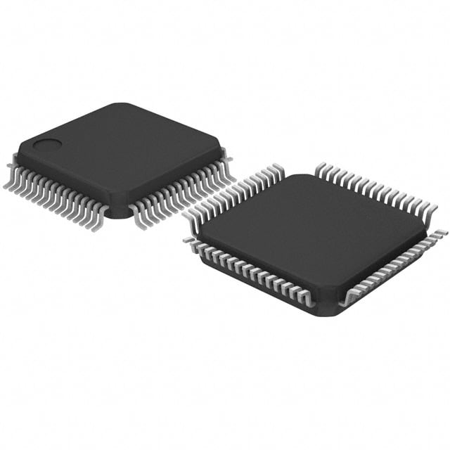
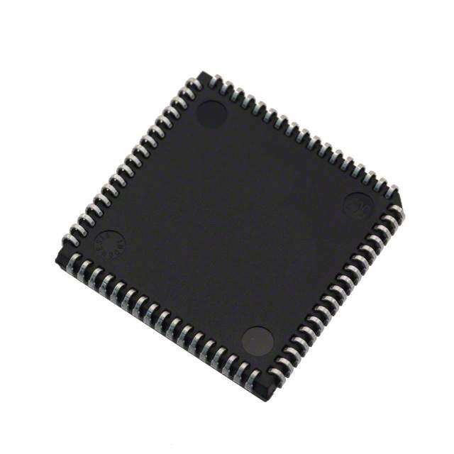
| 供应商器件封装 | 64-LQFP(10x10) |
| 其它名称 | 568-3284 |
| 包装 | 托盘 |
| 协议 | - |
| 安装类型 | 表面贴装 |
| 封装/外壳 | 64-LQFP |
| 带CMOS | 是 |
| 带IrDA编码器/解码器 | - |
| 带假起始位检测 | 是 |
| 带并行端口 | - |
| 带自动流量控制 | 是 |
| 带调制解调器控制 | 是 |
| 标准包装 | 160 |
| 特性 | - |
| 电压-电源 | 2.5V,3.3V,5V |
| 通道数 | 1,UART |


- 商务部:美国ITC正式对集成电路等产品启动337调查
- 曝三星4nm工艺存在良率问题 高通将骁龙8 Gen1或转产台积电
- 太阳诱电将投资9.5亿元在常州建新厂生产MLCC 预计2023年完工
- 英特尔发布欧洲新工厂建设计划 深化IDM 2.0 战略
- 台积电先进制程称霸业界 有大客户加持明年业绩稳了
- 达到5530亿美元!SIA预计今年全球半导体销售额将创下新高
- 英特尔拟将自动驾驶子公司Mobileye上市 估值或超500亿美元
- 三星加码芯片和SET,合并消费电子和移动部门,撤换高东真等 CEO
- 三星电子宣布重大人事变动 还合并消费电子和移动部门
- 海关总署:前11个月进口集成电路产品价值2.52万亿元 增长14.8%


PDF Datasheet 数据手册内容提取
SC16C750B 5 V, 3.3 V and 2.5 V UART with 64-byte FIFOs Rev. 05 — 17 October 2008 Product data sheet 1. General description TheSC16C750BisaUniversalAsynchronousReceiverandTransmitter(UART)usedfor serial data communications. Its principal function is to convert parallel data into serial data, and vice versa. The UART can handle serial data rates up to 3Mbit/s. The SC16C750B is pin compatible with the TL16C750 and it will power-up to be functionally equivalent to the 16C450. Programming of control registers enables the addedfeaturesoftheSC16C750B.Someoftheseaddedfeaturesarethe64-bytereceive and transmit FIFOs, automatic hardware flow control. The selectable auto-flow control feature significantly reduces software overload and increases system efficiency while in FIFO mode by automatically controlling serial data flow usingRTS output andCTS input signals. The SC16C750B also provides DMA mode data transfers through FIFO trigger levels and theTXRDY andRXRDY signals. On-board status registers provide the user with error indications, operational status, and modem interface control. System interrupts may be tailored to meet user requirements. An internal loopback capability allows on-board diagnostics. TheSC16C750Boperatesat5V,3.3Vand2.5V,theindustrialtemperaturerangeandis available in plastic PLCC44, LQFP64, and HVQFN32 packages. 2. Features n Single channel n 5V, 3.3V and 2.5V operation n 5V tolerant on input only pins1 n Industrial temperature range (- 40(cid:176) C to +85(cid:176) C) n After reset, all registers are identical to the typical 16C450 register set n Capable of running with all existing generic 16C450 software n Pin compatibility with the industry-standard ST16C450/550, TL16C450/550, PC16C450/550. Software compatible with SC16C750 and TL16C750 n Upto3Mbit/stransmit/receiveoperationat5V,2Mbit/sat3.3V,and1Mbit/sat2.5V n 64-byte transmit FIFO n 64-byte receive FIFO with error flags n Programmable auto-RTS and auto-CTS u In auto-CTS mode,CTS controls transmitter u In auto-RTS mode, receive FIFO contents and threshold controlRTS n Automatic hardware flow control n Software selectable baud rate generator 1. For data bus pins D7 to D0, seeTable 24 “Limiting values”.
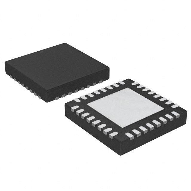
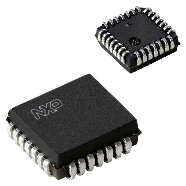
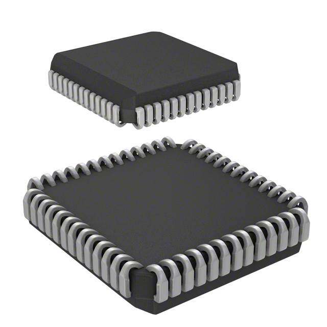
SC16C750B NXP Semiconductors 5 V, 3.3 V and 2.5 V UART with 64-byte FIFOs n Four selectable Receive interrupt trigger levels n Standard modem interface n Sleep mode n Standard asynchronous error and framing bits (Start, Stop, and Parity Overrun Break) n Independent receiver clock input n Transmit, Receive, Line Status, and data set interrupts independently controlled n Fully programmable character formatting: u 5-bit, 6-bit, 7-bit, or 8-bit characters u Even, odd, or no-parity formats u 1, 11⁄ , or 2-stop bit 2 u Baud generation (DC to 3Mbit/s) n False start-bit detection n Complete status reporting capabilities n 3-state output TTL drive capabilities for bidirectional data bus and control bus n Line break generation and detection n Internal diagnostic capabilities: u Loopback controls for communications link fault isolation n Prioritized interrupt system controls n Modem control functions (CTS,RTS,DSR,DTR,RI,DCD) 3. Ordering information Table 1. Ordering information Industrial: V =2.5V, 3.3V or 5V– 10%; T =- 40(cid:176) C to +85(cid:176) C. CC amb Type number Package Name Description Version SC16C750BIA44 PLCC44 plastic leaded chip carrier; 44 leads SOT187-2 SC16C750BIB64 LQFP64 plastic low profile quad flat package; 64 leads; 10· 10· 1.4mm SOT314-2 SC16C750BIBS HVQFN32 plastic thermal enhanced very thin quad flat package; no leads; SOT617-1 32terminals; body 5· 5· 0.85mm SC16C750B_5 © NXP B.V. 2008. All rights reserved. Product data sheet Rev. 05 — 17 October 2008 2 of 44
SC16C750B NXP Semiconductors 5 V, 3.3 V and 2.5 V UART with 64-byte FIFOs 4. Block diagram SC16C750B TRANSMIT TRANSMIT FIFO SHIFT TX REGISTERS REGISTER D0 to D7 DATA BUS IOR, IOR AND IOW, IOW CONTROL RESET LOGIC FLOW CONTROL LOGIC S E RECEIVE RECEIVE S LIN ALS REGFIISFTOERS RESGHISIFTTER RX U N B G T DSI CS0, CAS01 ,t oC AASS22 RSELEGOLIGSETICCETR NTERCONNECANCONTROL COLFONLOGTRWICOL I DDIS DTR RTS OUT1, OUT2 MODEM CONTROL LOGIC CTS INT INTERRUPT CLOCK AND RI TXRDY CONTROL BAUD RATE DCD RXRDY LOGIC GENERATOR DSR 002aaa588 XTAL1 XTAL2 RCLK BAUDOUT Shown for PLCC44 and LQFP64 pin assignments. Fig 1. Block diagram of SC16C750B SC16C750B_5 © NXP B.V. 2008. All rights reserved. Product data sheet Rev. 05 — 17 October 2008 3 of 44
SC16C750B NXP Semiconductors 5 V, 3.3 V and 2.5 V UART with 64-byte FIFOs 5. Pinning information 5.1 Pinning D4 D3 D2 D1 D0 n.c. VCC RI DCD DSR CTS 6 5 4 3 2 1 44 43 42 41 40 D5 7 39 RESET D6 8 38 OUT1 D7 9 37 DTR RCLK 10 36 RTS RX 11 35 OUT2 n.c. 12 SC16C750BIA44 34 n.c. TX 13 33 INT CS0 14 32 RXRDY CS1 15 31 A0 CS2 16 30 A1 BAUDOUT 17 29 A2 8 9 0 1 2 3 4 5 6 7 8 1 1 2 2 2 2 2 2 2 2 2 002aaa589 XTAL1 XTAL2 IOW IOW GND n.c. IOR IOR DDIS TXRDY AS Fig 2. Pin configuration for PLCC44 terminal 1 4 3 2 1 0 CC SR TS index area D D D D D V D C 2 1 0 9 8 7 6 5 3 3 3 2 2 2 2 2 D5 1 24 RESET D6 2 23 OUT D7 3 22 DTR RCLK 4 21 RTS SC16C750BIBS RX 5 20 INT TX 6 19 RXRDY CS 7 18 A0 BAUDOUT 8 17 A1 9 10 11 12 13 14 15 16 XTAL1 XTAL2 IOW n.c. GND IOR TXRDY A2 002aaa949 Transparent top view Fig 3. Pin configuration for HVQFN32 SC16C750B_5 © NXP B.V. 2008. All rights reserved. Product data sheet Rev. 05 — 17 October 2008 4 of 44
SC16C750B NXP Semiconductors 5 V, 3.3 V and 2.5 V UART with 64-byte FIFOs T U O D K AU c. S2 S1 c. S0 X c. c. X CL c. 7 6 5 c. B n. C C n. C T n. n. R R n. D D D n. 4 3 2 1 0 9 8 7 6 5 4 3 2 1 0 9 6 6 6 6 6 5 5 5 5 5 5 5 5 5 5 4 XTAL1 1 48 D4 XTAL2 2 47 n.c. n.c. 3 46 D3 IOW 4 45 D2 n.c. 5 44 n.c. IOW 6 43 D1 n.c. 7 42 D0 GND 8 41 n.c. SC16C750BIB64 IOR 9 40 VCC IOR 10 39 n.c. n.c. 11 38 RI DDIS 12 37 n.c. TXRDY 13 36 DCD n.c. 14 35 DSR AS 15 34 n.c. n.c. 16 33 CTS 7 8 9 0 1 2 3 4 5 6 7 8 9 0 1 2 1 1 1 2 2 2 2 2 2 2 2 2 2 3 3 3 002aaa590 A2 A1 n.c. A0 RDY n.c. INT n.c. UT2 RTS n.c. DTR n.c. UT1 n.c. SET X O O E R R Fig 4. Pin configuration for LQFP64 5.2 Pin description Table 2. Pin description Symbol Pin Type Description PLCC44 LQFP64 HVQFN32 A2, A1, A0 29, 30, 17, 18, 20 16, 17, 18 I Register select. A0 to A2 are used during read and write 31 operations to select the UART register to read from or write to. Refer toTable3 for register addresses and refer toAS description. AS 28 15 - I Address strobe. WhenAS is active (LOW), A0, A1, and A2 and CS0,CS1,andCS2drivetheinternalselectlogicdirectly;whenAS is HIGH, the register select and chip select signals are held at the logic levels they were in when the LOW-to-HIGH transition ofAS occurred. BAUDOUT 17 64 8 O Baud out.BAUDOUT is a 16· clock signal for the transmitter section of the UART. The clock rate is established by the reference oscillator frequency divided by a divisor specified in the baud rate generator divisor latches.BAUDOUT may also be used for the receiver section by tying this output to RCLK. CS0,CS1, 14, 15, 59, 61, 62 - I Chipselect.WhenCS0andCS1areHIGHandCS2isLOW,these CS2 16 threeinputsselecttheUART.Whenanyoftheseinputsareinactive, the UART remains inactive (refer toAS description). CS - - 7 I SC16C750B_5 © NXP B.V. 2008. All rights reserved. Product data sheet Rev. 05 — 17 October 2008 5 of 44
SC16C750B NXP Semiconductors 5 V, 3.3 V and 2.5 V UART with 64-byte FIFOs Table 2. Pin description …continued Symbol Pin Type Description PLCC44 LQFP64 HVQFN32 CTS 40 33 25 I Clear to send.CTS is a modem status signal. Its condition can be checked by reading bit4 (CTS) of the Modem Status Register (MSR). MSR[3] (D CTS) indicates thatCTS has changed states since the last read from the MSR. If the modem status interrupt is enabled whenCTS changes levels and the auto-CTS mode is not enabled, an interrupt is generated.CTS is also used in the auto-CTS mode to control the transmitter. D7 to D0 9, 8, 7, 52,51,50, 3,2,1,32, I/O Data bus. Eight data lines with 3-state outputs provide a 6, 5, 4, 48,46,45, 31, 30, bidirectional path for data, control and status information between 3, 2 43, 42 29, 28 the UART and the CPU. DCD 42 36 - I Data carrier detect.DCD is a modem status signal. Its condition can be checked by reading bit7 (DCD) of the Modem Status Register (MSR). MSR[3] (D DCD) indicates thatDCD has changed states since the last read from the MSR. If the modem status interrupt is enabled whenDCD changes levels, an interrupt is generated. DDIS 26 12 - O Driver disable.DDIS is active (LOW) when the CPU is reading data. When inactive (HIGH),DDIS can disable an external transceiver. DSR 41 35 26 I Datasetready.DSRisamodemstatussignal.Itsconditioncanbe checkedbyreadingbit5(DSR)oftheModemStatusRegister.Bit1 (DDSR) of the MSR indicatesDSR has changed levels since the last read from the MSR. If the modem status interrupt is enabled whenDSR changes levels, an interrupt is generated. DTR 37 28 22 O Data terminal ready. When active (LOW),DTR informs a modem ordatasetthattheUARTisreadytoestablishcommunication.DTR is placed in the active level by setting theDTR bit of the Modem Control Register.DTR is placed in the inactive level either as a result of a Master Reset, during Loopback mode operation, or clearing theDTR bit. INT 33 23 20 O Interrupt.Whenactive(HIGH),INTinformstheCPUthattheUART has an interrupt to be serviced. Four conditions that cause an interrupt to be issued are: a receiver error, received data that is available or timed out (FIFO mode only), an empty transmitter holding register or an enabled modem status interrupt. INT is reset (deactivated)eitherwhentheinterruptisservicedorasaresultofa Master Reset. n.c. 34 3,5,7,11, 12 - not connected 14,16,19, 22,24,27, 29,31,34, 37,39,41, 44,47,49, 53,56,57, 60, 63 OUT1, 38, 35 30, 25 - O Outputs 1 and 2. These are user-designated output terminals that OUT2 are set to the active (LOW) level by setting respective Modem Control Register (MCR) bits (OUT1 andOUT2).OUT1 andOUT2 OUT - - 23 O are set to inactive the (HIGH) level as a result of Master Reset, during Loopback mode operations, or by clearing bit2 (OUT1) or bit3 (OUT2) of the MCR. SC16C750B_5 © NXP B.V. 2008. All rights reserved. Product data sheet Rev. 05 — 17 October 2008 6 of 44
SC16C750B NXP Semiconductors 5 V, 3.3 V and 2.5 V UART with 64-byte FIFOs Table 2. Pin description …continued Symbol Pin Type Description PLCC44 LQFP64 HVQFN32 RCLK 10 54 4 I Receiver clock. RCLK is the 16· baud rate clock for the receiver section of the UART. RESET 39 32 24 I Master Reset. When active (HIGH), RESET clears most UART registers and sets the levels of various output signals. IOR 25 10 - I Read inputs. When eitherIOR or IOR is active (LOW or HIGH, respectively) while the UART is selected, the CPU is allowed to IOR 24 9 14 I readstatusinformationordatafromaselectedUARTregister.Only oneoftheseinputsisrequiredforthetransferofdataduringaread operation; the other input should be tied to its inactive level (that is, IOR tied LOW orIOR tied HIGH). RI 43 38 - I Ring indicator.RI is a modem status signal. Its condition can be checked by reading bit6 (RI) of the Modem Status Register. Bit2 (D RI) of the MSR indicates thatRI has changed from a LOW to a HIGH level since the last read from the MSR. If the modem status interrupt is enabled when this transition occurs, an interrupt is generated. RTS 36 26 21 O Request to send. When active,RTS informs the modem or data set that the UART is ready to receive data.RTS is set to the active level by setting theRTS Modem Control Register bit and is set to the inactive (HIGH) level either as a result of a Master Reset or during Loopback mode operations or by clearing bit 1 (RTS) of the MCR. In the auto-RTS mode,RTS is set to the inactive level by the receiver threshold control logic. RXRDY 32 21 19 O Receiver ready. Receiver Direct Memory Access (DMA) signaling isavailablewithRXRDY.WhenoperatingintheFIFOmode,oneof twotypesofDMAsignalingcanbeselectedusingtheFIFOControl Register bit3 (FCR[3]). When operating in the 16C450 mode, only DMA mode0 is allowed. Mode 0 supports single-transfer DMA in which a transfer is made between CPU bus cycles. Mode 1 supports multi-transfer DMA in which multiple transfers are made continuously until the receiver FIFO has been emptied. In DMA mode 0 (FCR[0]=0 or FCR[0]=1, FCR[3]=0), when there is at leastonecharacterinthereceiverFIFOorreceiverholdingregister, RXRDY is active (LOW). WhenRXRDY has been active but there are no characters in the FIFO or holding register,RXRDY goes inactive (HIGH). In DMA mode1 (FCR[0]=1, FCR[3]=1), when the trigger level or the time-out has been reached,RXRDY goes active (LOW); when it has been active but there are no more characters in the FIFO or holding register, it goes inactive (HIGH). RX 11 55 5 I Serial data input. RX is serial data input from a connected communications device. TX 13 58 6 O Serial data output. TX is composite serial data output to a connected communication device. TX is set to the marking (HIGH) level as a result of Master Reset. SC16C750B_5 © NXP B.V. 2008. All rights reserved. Product data sheet Rev. 05 — 17 October 2008 7 of 44
SC16C750B NXP Semiconductors 5 V, 3.3 V and 2.5 V UART with 64-byte FIFOs Table 2. Pin description …continued Symbol Pin Type Description PLCC44 LQFP64 HVQFN32 TXRDY 27 13 15 O Transmitter ready. Transmitter DMA signaling is available with TXRDY. When operating in the FIFO mode, one of two types of DMA signaling can be selected using FCR[3]. When operating in the 16C450 mode, only DMA mode0 is allowed. Mode0 supports single-transfer DMA in which a transfer is made between CPU bus cycles. Mode1 supports multi-transfer DMA in which multiple transfers are made continuously until the transmit FIFO has been filled. V 44 40 27 Power 2.5V, 3V or 5V supply voltage. CC GND 22 8 13 Power Ground voltage. IOW 21 6 - I Write inputs. When eitherIOW or IOW is active (LOW or HIGH, respectively)andwhiletheUARTisselected,theCPUisallowedto IOW 20 4 11 I writecontrolwordsordataintoaselectedUARTregister.Onlyone of these inputs is required to transfer data during a write operation; the other input should be tied to its inactive level (that is, IOW tied LOW orIOW tied HIGH). XTAL1 18 1 9 I Crystal connection or External clock input. XTAL2[1] 19 2 10 O Crystal connection or the inversion of XTAL1 if XTAL1 is driven. [1] In Sleep mode, XTAL2 is left floating. 6. Functional description TheSC16C750B provides serial asynchronous receive data synchronization, parallel-to-serial and serial-to-parallel data conversions for both the transmitter and receiversections.Thesefunctionsarenecessaryforconvertingtheserialdatastreaminto parallel data that is required with digital data systems. Synchronization for the serial data stream is accomplished by adding start and stop bits to the transmit data to form a data character(characterorientatedprotocol).Dataintegrityisinsuredbyattachingaparitybit to the data character. The parity bit is checked by the receiver for any transmission bit errors. TheSC16C750B is fabricated with an advanced CMOS process to achieve low drain power and high speed requirements. TheSC16C750B is an upward solution that provides 64bytes of transmit and receive FIFO memory, instead of none in the 16C450, or 16bytes in the 16C550. The SC16C750B is designed to work with high speed modems and shared network environmentsthatrequirefastdataprocessingtime.Increasedperformanceisrealizedin theSC16C750B by the larger transmit and receive FIFOs. This allows the external processor to handle more networking tasks within a given time. In addition, the four selectablelevelsofFIFOtriggerinterruptandautomatichardwareflowcontrolisuniquely provided for maximum data throughput performance, especially when operating in a multi-channel environment. The combination of the above greatly reduces the bandwidth requirement of the external controlling CPU, increases performance, and reduces power consumption. TheSC16C750Biscapableofoperationupto3Mbit/switha48MHzexternalclockinput (at 5V). SC16C750B_5 © NXP B.V. 2008. All rights reserved. Product data sheet Rev. 05 — 17 October 2008 8 of 44
SC16C750B NXP Semiconductors 5 V, 3.3 V and 2.5 V UART with 64-byte FIFOs The rich feature set of theSC16C750B is available through internal registers. Automatic hardware flow control, selectable transmit and receive FIFO trigger level, selectable TX and RX baud rates, modem interface controls, and a sleep mode are some of these features. 6.1 Internal registers TheSC16C750Bprovides12internalregistersformonitoringandcontrol.Theseregisters are shown inTable3. These twelve registers are similar to those already available in the standard16C550.Theseregistersfunctionasdataholdingregisters(THR/RHR),interrupt status and control registers (IER/ISR), a FIFO Control Register (FCR), line status and control registers (LCR/LSR), modem status and control registers (MCR/MSR), programmable data rate (clock) control registers (DLL/DLM), and a user accessible Scratchpad Register (SPR). Register functions are more fully described in the following paragraphs. Table 3. Internal registers decoding A2 A1 A0 READ mode WRITE mode General register set (THR/RHR, IER/ISR, MCR/MSR, FCR, LSR, SPR)[1] 0 0 0 Receive Holding Register Transmit Holding Register 0 0 1 Interrupt Enable Register Interrupt Enable Register 0 1 0 Interrupt Status Register FIFO Control Register 0 1 1 Line Control Register Line Control Register 1 0 0 Modem Control Register Modem Control Register 1 0 1 Line Status Register n/a 1 1 0 Modem Status Register n/a 1 1 1 Scratchpad Register Scratchpad Register Baud rate register set (DLL/DLM)[2] 0 0 0 LSB of Divisor Latch LSB of Divisor Latch 0 0 1 MSB of Divisor Latch MSB of Divisor Latch [1] These registers are accessible only when LCR[7] is a logic0. [2] These registers are accessible only when LCR[7] is a logic1. SC16C750B_5 © NXP B.V. 2008. All rights reserved. Product data sheet Rev. 05 — 17 October 2008 9 of 44
SC16C750B NXP Semiconductors 5 V, 3.3 V and 2.5 V UART with 64-byte FIFOs 6.2 FIFO operation The 64-byte transmit and receive data FIFOs are enabled by the FIFO Control Register bit0 (FCR[0]). The receiver FIFO section includes a time-out function to ensure data is delivered to the external CPU. An interrupt is generated whenever the Receive Holding Register (RHR) has not been read following the loading of a character or the receive trigger level has not been reached. Table 4. Flow control mechanism Selected trigger level INT pin activation NegateRTS AssertRTS (characters) 16-byte FIFO 1 1 1 0 4 4 4 0 8 8 8 0 14 14 14 0 64-byte FIFO 1 1 1 0 16 16 16 0 32 32 32 0 56 56 56 0 6.3 Hardware flow control Whenautomatichardwareflowcontrolisenabled,theSC16C750BmonitorstheCTSpin for a remote buffer overflow indication and controls theRTS pin for local buffer overflows. Automatic hardware flow control is selected by setting MCR[5] (RTS) and MCR[1] (CTS) to a logic1. IfCTS transitions from a logic0 to a logic1 indicating a flow control request, theSC16C750BwillsuspendTXtransmissionsassoonasthestopbitofthecharacterin process is shifted out. Transmission is resumed after theCTS input returns to a logic0, indicating more data may be sent. With the auto-RTS function enabled, an interrupt is generated when the receive FIFO reaches the programmed trigger level. TheRTS pin will not be forced to a logic1 (RTS off),untilthereceiveFIFOreachesthenexttriggerlevel.However,theRTSpinwillreturn to a logic0 after the data buffer (FIFO) is emptied. However, under the above described conditions, the SC16C750B will continue to accept data until the receive FIFO is full. 6.4 Time-out interrupts When two interrupt conditions have the same priority, it is important to service these interrupts correctly. Receive Data Ready and Receive Time-Out have the same interrupt priority (when enabled by IER[0]). The receiver issues an interrupt after the number of characters have reached the programmed trigger level. In this case, theSC16C750B FIFOmayholdmorecharactersthantheprogrammedtriggerlevel.Followingtheremoval of a data byte, the user should re-check LSR[0] for additional characters. A Receive Time-Out will not occur if the receive FIFO is empty. The time-out counter is reset at the center of each stop bit received or each time the receive holding register (RHR) is read. The actual time-out value is 4 character time. SC16C750B_5 © NXP B.V. 2008. All rights reserved. Product data sheet Rev. 05 — 17 October 2008 10 of 44
SC16C750B NXP Semiconductors 5 V, 3.3 V and 2.5 V UART with 64-byte FIFOs 6.5 Programmable baud rate generator TheSC16C750B supports high speed modem technologies that have increased input data rates by employing data compression schemes. For example, a 33.6kbit/s modem that employs data compression may require a 115.2kbit/s input data rate. A128.0kbit/s ISDNmodemthatsupportsdatacompressionmayneedaninputdatarateof460.8kbit/s. A single baud rate generator is provided for the transmitter and receiver, allowing independentTX/RXchannelcontrol.Theprogrammablebaudrategeneratoriscapableof accepting an input clock up to 48MHz, as required for supporting a 3Mbit/s data rate. TheSC16C750B can be configured for internal or external clock operation. For internal clock oscillator operation, an industry standard microprocessor crystal (parallel resonant, 22pF to 33pF load) is connected externally between the XTAL1 and XTAL2 pins (see Figure5). Alternatively, an external clock can be connected to the XTAL1 pin to clock the internal baud rate generator for standard or custom rates (seeTable5). XTAL1 XTAL2 XTAL1 XTAL2 1.5 kW X1 X1 1.8432 MHz 1.8432 MHz C1 C2 C1 C2 22 pF 33 pF 22 pF 47 pF 002aaa870 Fig 5. Crystal oscillator connection The generator divides the input 16· clock by any divisor from 1 to (216- 1). The SC16C750B divides the basic crystal or external clock by 16. The frequency of the BAUDOUT output pin is exactly 16· (16 times) of the selected baud rate (BAUDOUT=16Baud Rate). Customized baud rates can be achieved by selecting the proper divisor values for the MSB and LSB sections of baud rate generator. Programming the baud rate generator registers DLM (MSB) and DLL (LSB) provides a user capability for selecting the desired final baud rate. The example inTable5 shows selectable baud rates when using a 1.8432MHz crystal. For custom baud rates, the divisor value can be calculated usingEquation1: XTAL1 clock frequency divisor (in decimal) = ---------------------------------------------------------------- (1) serial data rate· 16 SC16C750B_5 © NXP B.V. 2008. All rights reserved. Product data sheet Rev. 05 — 17 October 2008 11 of 44
SC16C750B NXP Semiconductors 5 V, 3.3 V and 2.5 V UART with 64-byte FIFOs Table 5. Baud rates using 1.8432MHz or 3.072MHz crystal Using 1.8432MHz crystal Using 3.072MHz crystal Desired Divisor for Baud rate Desired Divisor for Baud rate baudrate 16· clock error baudrate 16· clock error 50 2304 50 3840 75 1536 75 2560 110 1047 0.026 110 1745 0.026 134.5 857 0.058 134.5 1428 0.034 150 768 150 1280 300 384 300 640 600 192 600 320 1200 96 1200 160 1800 64 1800 107 0.312 2000 58 0.69 2000 96 2400 48 2400 80 3600 32 3600 53 0.628 4800 24 4800 40 7200 16 7200 27 1.23 9600 12 9600 20 19200 6 19200 10 38400 3 38400 5 56000 2 2.86 6.6 DMA operation TheSC16C750B FIFO trigger level provides additional flexibility to the user for block mode operation. The user can optionally operate the transmit and receive FIFOs in the DMA mode (FCR[3]). The DMA mode affects the state of theRXRDY andTXRDY output pins.Table6 andTable7 show this. Table 6. Effect of DMA mode on state ofRXRDY pin Non-DMA mode DMA mode 1=FIFO empty 0-to-1 transition when FIFO empties 0=at least 1 byte in FIFO 1-to-0 transition when FIFO reaches trigger level, ortime-out occurs Table 7. Effect of DMA mode on state ofTXRDY pin Non-DMA mode DMA mode 1=at least 1 byte in FIFO 0-to-1 transition when FIFO becomes full 0=FIFO empty 1-to-0 transition when FIFO becomes empty SC16C750B_5 © NXP B.V. 2008. All rights reserved. Product data sheet Rev. 05 — 17 October 2008 12 of 44
SC16C750B NXP Semiconductors 5 V, 3.3 V and 2.5 V UART with 64-byte FIFOs 6.7 Sleep mode TheSC16C750B is designed to operate with low power consumption. A special Sleep mode is included to further reduce power consumption (the internal oscillator driver is disabled) when the chip is not being used. With IER[4] enabled (set to a logic1), the SC16C750B enters the Sleep mode, but resumes normal operation when a start bit is detected,achangeofstateofRXoronanyofthemodeminputpinsRI,CTS,DSR,DCD, or a transmit data is provided by the user. If the Sleep mode is enabled and the SC16C750B is awakened by one of the conditions described above, it will return to the Sleepmodeautomaticallyafterthelastcharacteristransmittedorreadbytheuser.Inany case, the Sleep mode will not be entered while an interrupt(s) is pending. The SC16C750BwillstayintheSleepmodeofoperationuntilitisdisabledbysettingIER[4]to a logic0. 6.8 Low power mode In Low power mode the oscillator is still running and only the clock to the UART core is cutoff.Thishelpstoreducetheoperatingcurrenttoabout1⁄ .TheUARTwakesupunder 3 the same conditions as in Sleep mode. 6.9 Loopback mode The internal loopback capability allows on-board diagnostics. In the Loopback mode, the normal modem interface pins are disconnected and reconfigured for loopback internally. MCR[3:0] register bits are used for controlling loopback diagnostic testing. In the Loopbackmode,OUT1andOUT2intheMCRregister(bit2andbit3)controlthemodem RI andDCD inputs, respectively. MCR signalsDTR andRTS (bit0 and bit1) are used to controlthemodemDSRandCTSinputs,respectively.Thetransmitteroutput(TX)andthe receiverinput(RX)aredisconnectedfromtheirassociatedinterfacepins,andinsteadare connected together internally (seeFigure6). TheCTS,DSR,DCD, andRI are disconnected from their normal modem control input pins, and instead are connected internallytoRTS,DTR,OUT2andOUT1.LoopbacktestdataisenteredintotheTransmit Holding Register via the user data bus interface, D0toD7. The transmit UART serializes the data and passes the serial data to the receive UART via the internal loopback connection.ThereceiveUARTconvertstheserialdatabackintoparalleldatathatisthen made available at the user data interface D0toD7. The user optionally compares the received data to the initial transmitted data for verifying error-free operation of the UART TX/RX circuits. SC16C750B_5 © NXP B.V. 2008. All rights reserved. Product data sheet Rev. 05 — 17 October 2008 13 of 44
SC16C750B NXP Semiconductors 5 V, 3.3 V and 2.5 V UART with 64-byte FIFOs SC16C750B TRANSMIT TRANSMIT FIFO SHIFT TX REGISTERS REGISTER D0 to D7 DATA BUS IOR, IOR AND IOW, IOW CONTROL RESET LOGIC FLOW CONTROL MCR[4] = 1 LOGIC S E RECEIVE RECEIVE S LIN ALS REGFIISFTOERS RESGHISIFTTER RX U N B G T DSI CS0, CAS01 ,t oC AASS22 RSELEGOLIGSETICCETR NTERCONNECANCONTROL COLFONLOGTRWICOL I RTS DDIS CTS DTR DSR MODEM CONTROL OUT1 LOGIC INT INTERRUPT CLOCK AND TXRDY CONTROL BAUD RATE RXRDY LOGIC GENERATOR RI OUT2 DCD 002aaa591 XTAL1 XTAL2 RCLK BAUDOUT Shown for PLCC44 and LQFP64 pin assignments. Fig 6. Internal Loopback mode diagram SC16C750B_5 © NXP B.V. 2008. All rights reserved. Product data sheet Rev. 05 — 17 October 2008 14 of 44
SC16C750B NXP Semiconductors 5 V, 3.3 V and 2.5 V UART with 64-byte FIFOs 7. Register descriptions Table8detailstheassignedbitfunctionsforthefifteenSC16C750Binternalregisters.The assigned bit functions are more fully defined inSection7.1 throughSection7.10. Table 8. SC16C750B internal registers A2 A1 A0 Register Default[1] Bit 7 Bit 6 Bit 5 Bit 4 Bit 3 Bit 2 Bit 1 Bit 0 General Register Set[2] 0 0 0 RHR XX bit 7 bit 6 bit 5 bit 4 bit 3 bit 2 bit 1 bit 0 0 0 0 THR XX bit 7 bit 6 bit 5 bit 4 bit 3 bit 2 bit 1 bit 0 0 0 1 IER 00 0 0 Low Sleep modem receive transmit receive power mode status line holding holding mode interrupt status register register interrupt 0 1 0 FCR 00 RCVR RCVR 64-byte reserved DMA XMIT RCVR FIFO trigger trigger FIFO mode FIFO FIFO enable (MSB) (LSB) enable select reset reset 0 1 0 ISR 01 FIFOs FIFOs 64-byte 0 INT INT INT INT enabled enabled FIFO priority priority priority status enable bit2 bit1 bit0 0 1 1 LCR 00 divisor set break set even parity stop bits word word latch parity parity enable length length enable bit1 bit0 1 0 0 MCR 00 0 0 flow loopback OUT2 OUT1 RTS DTR control enable 1 0 1 LSR 60 FIFO trans. trans. break framing parity overrun receive data empty holding interrupt error error error data error empty ready 1 1 0 MSR X0 DCD RI DSR CTS D DCD D RI D DSR D CTS 1 1 1 SPR FF bit 7 bit 6 bit 5 bit 4 bit 3 bit 2 bit 1 bit 0 Special Register Set[3] 0 0 0 DLL XX bit 7 bit 6 bit 5 bit 4 bit 3 bit 2 bit 1 bit 0 0 0 1 DLM XX bit 15 bit 14 bit 13 bit 12 bit 11 bit 10 bit 9 bit 8 [1] The value shown represents the register’s initialized HEX value; X=n/a. [2] These registers are accessible only when LCR[7]=0. [3] The Special Register set is accessible only when LCR[7] is set to a logic1. SC16C750B_5 © NXP B.V. 2008. All rights reserved. Product data sheet Rev. 05 — 17 October 2008 15 of 44
SC16C750B NXP Semiconductors 5 V, 3.3 V and 2.5 V UART with 64-byte FIFOs 7.1 Transmit Holding Register (THR) and Receive Holding Register (RHR) The serial transmitter section consists of an 8-bit Transmit Hold Register (THR) and Transmit Shift Register (TSR). The status of the THR is provided in the Line Status Register(LSR).WritingtotheTHRtransfersthecontentsofthedatabus(D7toD0)tothe THR,providingthattheTHRorTSRisempty.TheTHRemptyflagintheLSRregisterwill be set to a logic1 when the transmitter is empty or when data is transferred to the TSR. Note that a write operation can be performed when the THR empty flag is set (logic0=FIFO full; logic1=at least one FIFO location available). The serial receive section also contains an 8-bit Receive Holding Register (RHR). Receive data is removed from theSC16C750B and receive FIFO by reading the RHR register. The receive section provides a mechanism to prevent false starts. On the falling edge of a start or false start bit, an internal receiver counter starts counting clocks at the 16· clock rate. After 71⁄ clocks, the start bit time should be shifted to the center of the 2 start bit. At this time the start bit is sampled, and if it is still a logic0 it is validated. Evaluating the start bit in this manner prevents the receiver from assembling a false character. Receiver status codes will be posted in the LSR. 7.2 Interrupt Enable Register (IER) The Interrupt Enable Register (IER) masks the interrupts from receiver ready, transmitter empty, line status and modem status registers. These interrupts would normally be seen on the INT output pin. Table 9. Interrupt Enable Register bits description Bit Symbol Description 7:6 IER[7:6] Not used. 5 IER[5] Low power mode. logic0=disable Low power mode (normal default condition) logic1=enable Low power mode 4 IER[4] Sleep mode. logic0=disable Sleep mode (normal default condition) logic1=enable Sleep mode. SeeSection 6.7 “Sleep mode” for details. 3 IER[3] Modem Status Interrupt. logic0=disable the modem status register interrupt (normal default condition) logic1=enable the modem status register interrupt 2 IER[2] Receive Line Status interrupt. This interrupt will be issued whenever a fully assembled receive character is transferred from RSR to the RHR/FIFO, i.e., data ready, LSR[0]. logic0=disable the receiver line status interrupt (normal default condition) logic1=enable the receiver line status interrupt SC16C750B_5 © NXP B.V. 2008. All rights reserved. Product data sheet Rev. 05 — 17 October 2008 16 of 44
SC16C750B NXP Semiconductors 5 V, 3.3 V and 2.5 V UART with 64-byte FIFOs Table 9. Interrupt Enable Register bits description …continued Bit Symbol Description 1 IER[1] Transmit Holding Register interrupt. This interrupt will be issued whenever the THR is empty, and is associated with LSR[1]. logic0=disable the transmitter empty interrupt (normal default condition) logic1=enable the transmitter empty interrupt 0 IER[0] ReceiveHoldingRegisterinterrupt.ThisinterruptwillbeissuedwhentheFIFO has reached the programmed trigger level, or is cleared when the FIFO drops below the trigger level in the FIFO mode of operation. logic0=disable the receiver ready interrupt (normal default condition) logic1=enable the receiver ready interrupt 7.2.1 IER versus Receive FIFO interrupt mode operation When the receive FIFO (FCR[0]=logic1), and receive interrupts (IER[0]=logic1) are enabled, the receive interrupts and register status will reflect the following: • The receive data available interrupts are issued to the external CPU when the FIFO has reached the programmed trigger level. It will be cleared when the FIFO drops below the programmed trigger level. • FIFO status will also be reflected in the user accessible ISR register when the FIFO trigger level is reached. Both the ISR register status bit and the interrupt will be cleared when the FIFO drops below the trigger level. • The data ready bit (LSR[0]) is set as soon as a character is transferred from the shift register to the receive FIFO. It is reset when the FIFO is empty. 7.2.2 IER versus Receive/Transmit FIFO polled mode operation When FCR[0]=logic1, resetting IER[3:0] enables theSC16C750B in the FIFO polled mode of operation. Since the receiver and transmitter have separate bits in the LSR, either or both can be used in the polled mode by selecting respective transmit or receive control bit(s). • LSR[0] will be a logic1 as long as there is onebyte in the receive FIFO. • LSR[4:1] will provide the type of errors encountered, if any. • LSR[5] will indicate when the transmit FIFO is empty. • LSR[6]willindicatewhenboththetransmitFIFOandtransmitshiftregisterareempty. • LSR[7] will indicate any FIFO data errors. SC16C750B_5 © NXP B.V. 2008. All rights reserved. Product data sheet Rev. 05 — 17 October 2008 17 of 44
SC16C750B NXP Semiconductors 5 V, 3.3 V and 2.5 V UART with 64-byte FIFOs 7.3 FIFO Control Register (FCR) This register is used to enable the FIFOs, clear the FIFOs, set the receive FIFO trigger levels, and select the DMA mode. 7.3.1 DMA mode 7.3.1.1 Mode 0 (FCR bit 3=0) Setandenabletheinterruptforeachsingletransmitorreceiveoperation,andissimilarto the 16C450 mode. Transmit Ready (TXRDY) will go to a logic0 whenever an empty transmit space is available in the Transmit Holding Register (THR). Receive Ready (RXRDY)willgotoalogic0whenevertheReceiveHoldingRegister(RHR)isloadedwith a character. 7.3.1.2 Mode 1 (FCR bit 3=1) Setandenabletheinterruptinablockmodeoperation.Thetransmitinterruptissetwhen thetransmitFIFOisbelowtheprogrammedtriggerlevel.Thereceiveinterruptissetwhen the receive FIFO fills to the programmed trigger level. However, the FIFO continues to fill regardlessoftheprogrammedleveluntiltheFIFOisfull.RXRDYremainsalogic0aslong as the FIFO fill level is above the programmed trigger level. 7.3.2 FIFO mode Table 10. FIFO Control Register bits description Bit Symbol Description 7:6 FCR[7] RCVR trigger. These bits are used to set the trigger level for the receive (MSB), FIFO interrupt. FCR[6] (LSB) AninterruptisgeneratedwhenthenumberofcharactersintheFIFOequals theprogrammedtriggerlevel.However,theFIFOwillcontinuetobeloaded until it is full. Refer toTable11. 5 FCR[5] 64-byte FIFO enable. logic0=16-byte mode (normal default condition) logic1=64-byte mode 4 FCR[4] reserved 3 FCR[3] DMA mode select. logic0=set DMA mode ‘0’ (normal default condition). logic1=set DMA mode ‘1’ Transmit operation in mode ‘0’: When the SC16C750B is in the 16C450 mode (FIFOs disabled; FCR[0]=logic0) or in the FIFO mode (FIFOs enabled; FCR[0]=logic1; FCR[3]=logic0), and when there are no charactersinthetransmitFIFOortransmitholdingregister,theTXRDYpin will be a logic0. Once active, theTXRDY pin will go to a logic1 after the first character is loaded into the transmit holding register. Receive operation in mode ‘0’: When the SC16C750B is in 16C450 mode,orintheFIFOmode(FCR[0]=logic1;FCR[3]=logic0)andthereis at least one character in the receive FIFO, theRXRDY pin will be a logic0. Once active, theRXRDY pin will go to a logic1 when there are no more characters in the receiver. SC16C750B_5 © NXP B.V. 2008. All rights reserved. Product data sheet Rev. 05 — 17 October 2008 18 of 44
SC16C750B NXP Semiconductors 5 V, 3.3 V and 2.5 V UART with 64-byte FIFOs Table 10. FIFO Control Register bits description …continued Bit Symbol Description FCR[3] Transmit operation in mode ‘1’: When the SC16C750B is in FIFO mode (continued) (FCR[0]=logic1; FCR[3]=logic1), theTXRDY pin will be a logic1 when the transmit FIFO is completely full. It will be a logic0 when the FIFO is emptied. Receive operation in mode ‘1’: When the SC16C750B is in FIFO mode (FCR[0]=logic1;FCR[3]=logic1)andthetriggerlevelhasbeenreached, or a Receive Time-Out has occurred, theRXRDY pin will go to a logic0. Once activated, it will go to a logic1 after there are no more characters in the FIFO. 2 FCR[2] XMIT FIFO reset. logic0=no FIFO transmit reset (normal default condition) logic1=clears the contents of the transmit FIFO and resets the FIFO counterlogic(thetransmitshiftregisterisnotclearedoraltered).Thisbit will return to a logic0 after clearing the FIFO. 1 FCR[1] RCVR FIFO reset. logic0=no FIFO receive reset (normal default condition) logic1=clears the contents of the receive FIFO and resets the FIFO counter logic (the receive shift register is not cleared or altered). This bit will return to a logic0 after clearing the FIFO. 0 FCR[0] FIFO enable. logic0=disable the transmit and receive FIFO (normal default condition) logic1=enable the transmit and receive FIFO Table 11. RCVR trigger levels FCR[7] FCR[6] RX FIFO trigger level (bytes) 16-byte operation 64-byte operation 0 0 1 1 0 1 4 16 1 0 8 32 1 1 14 56 SC16C750B_5 © NXP B.V. 2008. All rights reserved. Product data sheet Rev. 05 — 17 October 2008 19 of 44
SC16C750B NXP Semiconductors 5 V, 3.3 V and 2.5 V UART with 64-byte FIFOs 7.4 Interrupt Status Register (ISR) TheSC16C750Bprovidesfourlevelsofprioritizedinterruptstominimizeexternalsoftware interaction.TheInterruptStatusRegister(ISR)providestheuserwithfourinterruptstatus bits. Performing a read cycle on the ISR will provide the user with the highest pending interrupt level to be serviced. No other interrupts are acknowledged until the pending interrupt is serviced. Whenever the interrupt status register is read, the interrupt status is cleared. However, it should be noted that only the current pending interrupt is cleared by the read. A lower level interrupt may be seen after re-reading the interrupt status bits. Table 12 “Interrupt source” shows the data values (bit0tobit4) for the four prioritized interrupt levels and the interrupt sources associated with each of these interrupt levels. Table 12. Interrupt source Priority ISR[3] ISR[2] ISR[1] ISR[0] Source of the interrupt level 1 0 1 1 0 LSR (Receiver Line Status Register) 2 0 1 0 0 RXRDY (Received Data Ready) 2 1 1 0 0 RXRDY (Receive Data time-out) 3 0 0 1 0 TXRDY (Transmitter Holding Register Empty) 4 0 0 0 0 MSR (Modem Status Register) Table 13. Interrupt Status Register bits description Bit Symbol Description 7:6 ISR[7:6] FIFOs enabled. These bits are set to a logic0 when the FIFO is not being used. They are set to a logic1 when the FIFOs are enabled. logic0 or cleared=default condition 5 ISR[5] 64-byte FIFO enable. logic0=16-byte operation logic1=64-byte operation 4 ISR[4] not used 3:1 ISR[3:1] INT priority bit2tobit0. These bits indicate the source for a pending interrupt at interrupt priority levels 1, 2, and 3 (seeTable12). logic0 or cleared=default condition 0 ISR[0] INT status. logic0=an interrupt is pending and the ISR contents may be used as a pointer to the appropriate interrupt service routine logic1=no interrupt pending (normal default condition) SC16C750B_5 © NXP B.V. 2008. All rights reserved. Product data sheet Rev. 05 — 17 October 2008 20 of 44
SC16C750B NXP Semiconductors 5 V, 3.3 V and 2.5 V UART with 64-byte FIFOs 7.5 Line Control Register (LCR) The Line Control Register is used to specify the asynchronous data communication format.Thewordlength,thenumberofstopbits,andtheparityareselectedbywritingthe appropriate bits in this register. Table 14. Line Control Register bits description Bit Symbol Description 7 LCR[7] Divisor latch enable. The internal baud rate counter latch and Enhanced Feature mode enable. logic0=divisor latch disabled (normal default condition) logic1=divisor latch and enhanced feature register enabled 6 LCR[6] Set break. When enabled, the Break control bit causes a break condition to betransmitted(theTXoutputisforcedtoalogic0state).Thisconditionexists until disabled by setting LCR[6] to a logic0. logic0=no TX break condition (normal default condition) logic1=forces the transmitter output (TX) to a logic0 for alerting the remote receiver to a line break condition 5 LCR[5] Set parity. If the parity bit is enabled, LCR[5] selects the forced parity format. Programs the parity conditions (seeTable15). logic0=parity is not forced (normal default condition) LCR[5]=logic1andLCR[4]=logic0:paritybitisforcedtoalogic1forthe transmit and receive data LCR[5]=logic1andLCR[4]=logic1:paritybitisforcedtoalogic0forthe transmit and receive data 4 LCR[4] Even parity. If the parity bit is enabled with LCR[3] set to a logic1, LCR[4] selects the even or odd parity format. logic0=oddparityisgeneratedbyforcinganoddnumberoflogic1sinthe transmitted data. The receiver must be programmed to check the same format (normal default condition). logic1=even parity is generated by forcing an even number of logic1s in thetransmitteddata.Thereceivermustbeprogrammedtocheckthesame format. 3 LCR[3] Parity enable. Parity or no parity can be selected via this bit. logic0=no parity (normal default condition) logic1=a parity bit is generated during the transmission, receiver checks the data and parity for transmission errors 2 LCR[2] Stop bits. The length of stop bit is specified by this bit in conjunction with the programmed word length (seeTable16). logic0 or cleared=default condition 1:0 LCR[1:0] Word length bit1, bit0. These two bits specify the word length to be transmitted or received (seeTable17). logic0 or cleared=default condition SC16C750B_5 © NXP B.V. 2008. All rights reserved. Product data sheet Rev. 05 — 17 October 2008 21 of 44
SC16C750B NXP Semiconductors 5 V, 3.3 V and 2.5 V UART with 64-byte FIFOs Table 15. LCR[5] parity selection LCR[5] LCR[4] LCR[3] Parity selection X X 0 no parity 0 0 1 odd parity 0 1 1 even parity 1 0 1 force parity ‘1’ 1 1 1 forced parity ‘0’ Table 16. LCR[2] stop bit length LCR[2] Word length (bits) Stop bit length (bit times) 0 5, 6, 7, 8 1 1 5 11⁄ 2 1 6, 7, 8 2 Table 17. LCR[1:0] word length LCR[1] LCR[0] Word length (bits) 0 0 5 0 1 6 1 0 7 1 1 8 SC16C750B_5 © NXP B.V. 2008. All rights reserved. Product data sheet Rev. 05 — 17 October 2008 22 of 44
SC16C750B NXP Semiconductors 5 V, 3.3 V and 2.5 V UART with 64-byte FIFOs 7.6 Modem Control Register (MCR) This register controls the interface with the modem or a peripheral device. Table 18. Modem Control Register bits description Bit Symbol Description 7 MCR[7] reserved; set to 0 6 MCR[6] reserved; set to 0 5 MCR[5] AFE. This bit is the auto flow control enable. When this bit is set, the auto flow control is enabled. 4 MCR[4] Loopback. Enable the local Loopback mode (diagnostics). In this mode the transmitteroutput(TX)andthereceiverinput(RX),CTS,DSR,DCD,andRI aredisconnectedfromtheSC16C750BI/Opins.Internallythemodemdata and control pins are connected into a loopback data configuration (see Figure6). In this mode, the receiver and transmitter interrupts remain fully operational. The Modem Control Interrupts are also operational, but the interrupts’sourcesareswitchedtothelowerfourbitsoftheModemControl. Interrupts continue to be controlled by the IER register. logic0=disable Loopback mode (normal default condition) logic1=enable local Loopback mode (diagnostics) 3 MCR[3] OUT2,INTenable.UsedtocontrolthemodemDCDsignalintheLoopback mode. logic0=setOUT2 to HIGH. In the Loopback mode, setsOUT2 (DCD) internally to a logic1. logic1=setOUT2 to LOW. In the Loopback mode, setsOUT2 (DCD) internally to a logic0. 2 MCR[2] OUT1. This bit is used in the Loopback mode only. In the Loopback mode, thisbitisusedtowritethestateofthemodemRIinterfacesignalviaOUT1. 1 MCR[1] RTS logic0=forceRTS output to a logic1 (normal default condition) logic1=forceRTS output to a logic0 0 MCR[0] DTR logic0=forceDTR output to a logic1 (normal default condition) logic1=forceDTR output to a logic0 The flow control can be configured by programming MCR[1] and MCR[5] as shown in Table19. Table 19. Flow control configuration MCR[5] (AFE) MCR[1] (RTS) Flow configuration 1 1 autoRTS andCTS enabled 1 0 autoCTS only enabled 0 X autoRTS andCTS disabled SC16C750B_5 © NXP B.V. 2008. All rights reserved. Product data sheet Rev. 05 — 17 October 2008 23 of 44
SC16C750B NXP Semiconductors 5 V, 3.3 V and 2.5 V UART with 64-byte FIFOs 7.7 Line Status Register (LSR) This register provides the status of data transfers between theSC16C750B and theCPU. Table 20. Line Status Register bits description Bit Symbol Description 7 LSR[7] FIFO data error. logic0=no error (normal default condition) logic1=at least one parity error, framing error or break indication is in the current FIFO data. This bit is cleared when LSR register is read. 6 LSR[6] THR and TSR empty. This bit is the Transmit Empty indicator. This bit is set to a logic1 whenever the transmit holding register and the transmit shift register are bothempty.Itisresettologic0whenevereithertheTHRorTSRcontainsadata character.IntheFIFOmode,thisbitissettologic1wheneverthetransmitFIFO and transmit shift register are both empty. 5 LSR[5] THR empty. This bit is the Transmit Holding Register Empty indicator. This bit indicates that the UART is ready to accept a new character for transmission. In addition, this bit causes the UART to issue an interrupt to CPU when the THR interrupt enable is set. The THR bit is set to a logic1 when a character is transferred from the transmit holding register into the transmitter shift register. The bit is reset to a logic0 concurrently with the loading of the transmitter holding register by the CPU. In the FIFO mode, this bit is set when the transmit FIFO is empty; it is cleared when at least 1byte is written to the transmit FIFO. 4 LSR[4] Break interrupt. logic0=no break condition (normal default condition) logic1=the receiver received a break signal (RX was a logic0 for one character frame time). In the FIFO mode, only one break character is loaded into the FIFO. 3 LSR[3] Framing error. logic0=no framing error (normal default condition) logic1=framingerror.Thereceivecharacterdidnothaveavalidstopbit(s).In the FIFO mode, this error is associated with the character at the top of the FIFO. 2 LSR[2] Parity error. logic0=no parity error (normal default condition) logic1=parity error. The receive character does not have correct parity informationandissuspect.IntheFIFOmode,thiserrorisassociatedwiththe character at the top of the FIFO. 1 LSR[1] Overrun error. logic0= no overrun error (normal default condition) logic1=overrun error. A data overrun error occurred in the receive shift register. This happens when additional data arrives while the FIFO is full. In thiscase,thepreviousdataintheshiftregisterisoverwritten.Notethatunder this condition, the data byte in the receive shift register is not transferred into the FIFO, therefore the data in the FIFO is not corrupted by the error. 0 LSR[0] Receive data ready. logic0= no data in receive holding register or FIFO (normal default condition) logic1=datahasbeenreceivedandissavedinthereceiveholdingregisteror FIFO SC16C750B_5 © NXP B.V. 2008. All rights reserved. Product data sheet Rev. 05 — 17 October 2008 24 of 44
SC16C750B NXP Semiconductors 5 V, 3.3 V and 2.5 V UART with 64-byte FIFOs 7.8 Modem Status Register (MSR) Thisregisterprovidesthecurrentstateofthecontrolinterfacesignalsfromthemodem,or other peripheral device to which theSC16C750B is connected. Fourbits of this register are used to indicate the changed information. These bits are set to a logic1 whenever a controlinputfromthemodemchangesstate.Thesebitsaresettoalogic0wheneverthe CPU reads this register. Table 21. Modem Status Register bits description Bit Symbol Description 7 MSR[7] Data Carrier Detect. DCD (activeHIGH, logic1). Normally this bit is the complement of theDCD input. In the Loopback mode this bit is equivalent to the OUT2 bit in the MCR register. 6 MSR[6] Ring Indicator. RI (activeHIGH, logic1). Normally this bit is the complement of theRI input. In the Loopback mode this bit is equivalent to the OUT1 bit in the MCR register. 5 MSR[5] Data Set Ready. DSR (activeHIGH, logic1). Normally this bit is the complement of theDSR input. In Loopback mode this bit is equivalent to the DTR bit in the MCR register. 4 MSR[4] Clear To Send. CTS.CTS functions as hardware flow control signal input if it is enabled via MCR[5]. Flow control (when enabled) allows starting and stopping the transmissions based on the external modemCTS signal. A logic1attheCTSpinwillstopSC16C750Btransmissionsassoonascurrent character has finished transmission. Normally MSR[4] is the complement of theCTS input. However, in the Loopback mode, this bit is equivalent to the RTS bit in the MCR register. 3 MSR[3] D DCD[1] logic0= noDCD change (normal default condition) logic1=theDCDinputtotheSC16C750Bhaschangedstatesincethelast time it was read. A modem Status Interrupt will be generated. 2 MSR[2] D RI[1] logic0= noRI change (normal default condition) logic1=theRI input to the SC16C750B has changed from a logic0 to a logic1. A modem Status Interrupt will be generated. 1 MSR[1] D DSR[1] logic0= noDSR change (normal default condition) logic1=theDSRinputtotheSC16C750Bhaschangedstatesincethelast time it was read. A modem Status Interrupt will be generated. 0 MSR[0] D CTS[1] logic0= noCTS change (normal default condition) logic1=theCTSinputtotheSC16C750Bhaschangedstatesincethelast time it was read. A modem Status Interrupt will be generated. [1] Whenever any MSR[0:3] is set to logic1, a Modem Status Interrupt will be generated. SC16C750B_5 © NXP B.V. 2008. All rights reserved. Product data sheet Rev. 05 — 17 October 2008 25 of 44
SC16C750B NXP Semiconductors 5 V, 3.3 V and 2.5 V UART with 64-byte FIFOs 7.9 Scratchpad Register (SPR) TheSC16C750B provides a temporary data register to store 8bits of user information. 7.10 SC16C750B external reset conditions Table 22. Reset state for registers Register Reset state IER IER[7:0]=0 ISR ISR[7:1]=0; ISR[0]=1 LCR LCR[7:0]=0 MCR MCR[7:0]=0 LSR LSR[7]=0; LSR[6:5]=1; LSR[4:0]=0 MSR MSR[7:4]=input signals; MSR[3:0]=0 FCR FCR[7:0]=0 Table 23. Reset state for outputs Output Reset state TX HIGH RTS HIGH DTR HIGH RXRDY HIGH (STD mode) TXRDY LOW (STD mode) INT LOW (STD mode) 8. Limiting values Table 24. Limiting values In accordance with the Absolute Maximum Rating System (IEC 60134). Symbol Parameter Conditions Min Max Unit V supply voltage - 7 V CC V voltage on any other pin at D7 to D0 pins GND- 0.3 V +0.3 V n CC at input only pins GND- 0.3 5.3 V T ambient temperature operating - 40 +85 (cid:176) C amb T storage temperature - 65 +150 (cid:176) C stg P /pack total power dissipation - 500 mW tot perpackage SC16C750B_5 © NXP B.V. 2008. All rights reserved. Product data sheet Rev. 05 — 17 October 2008 26 of 44
SC16C750B NXP Semiconductors 5 V, 3.3 V and 2.5 V UART with 64-byte FIFOs 9. Static characteristics Table 25. Static characteristics T =- 40(cid:176) C to +85(cid:176) C; tolerance of V =– 10%, unless otherwise specified. amb CC Symbol Parameter Conditions V =2.5V V =3.3V V =5.0V Unit CC CC CC Min Max Min Max Min Max V clock LOW-level input voltage - 0.3 0.45 - 0.3 0.6 - 0.5 0.6 V IL(clk) V clock HIGH-level input voltage 1.8 V 2.4 V 3.0 V V IH(clk) CC CC CC V LOW-level input voltage - 0.3 0.65 - 0.3 0.8 - 0.5 0.8 V IL V HIGH-level input voltage 1.6 - 2.0 - 2.2 V V IH CC V LOW-level output voltage on all outputs [1] OL I =5mA - - - - - 0.4 V OL (databus) I =4mA - - - 0.4 - - V OL (other outputs) I =2mA - 0.4 - - - - V OL (databus) I =1.6mA - 0.4 - - - - V OL (other outputs) V HIGH-level output voltage I =- 5mA - - - - 2.4 - V OH OH (databus) I =- 1mA - - 2.0 - - - V OH (other outputs) I =- 800m A 1.85 - - - - - V OH (databus) I =- 400m A 1.85 - - - - - V OH (other outputs) I LOW-level input leakage current - – 10 - – 10 - – 10 m A LIL I clock leakage current - – 30 - – 30 - – 30 m A L(clk) I average supply current - 3.5 - 4.5 - 4.5 mA CC(AV) I sleep mode supply current [2] - 50 - 50 - 50 m A CC(sleep) I low-power mode supply current - 1.0 - 1.5 - 1.5 mA CC(lp) C input capacitance - 5 - 5 - 5 pF i R internal pull-up resistance 500 - 500 - 500 - kW pu(int) [1] Except for XTAL2, V =1V typically. OL [2] Sleep current might be higher if there is activity on the UART databus during Sleep mode. SC16C750B_5 © NXP B.V. 2008. All rights reserved. Product data sheet Rev. 05 — 17 October 2008 27 of 44
SC16C750B NXP Semiconductors 5 V, 3.3 V and 2.5 V UART with 64-byte FIFOs 10. Dynamic characteristics Table 26. Dynamic characteristics T =- 40(cid:176) C to +85(cid:176) C; tolerance of V =– 10%, unless otherwise specified. amb CC Symbol Parameter Conditions V =2.5V V =3.3V V =5.0V Unit CC CC CC Min Max Min Max Min Max t clock pulse duration 15 - 13 - 10 - ns w1 t clock pulse duration 15 - 13 - 10 - ns w2 f frequency on pin XTAL1 [1] - 16 - 32 - 48 MHz XTAL1 t address strobe width 45 - 35 - 25 - ns 4w t address set-up time 5 - 5 - 1 - ns 5s t address hold time 5 - 5 - 5 - ns 5h t chip select set-up time toAS 10 - 5 - 0 - ns 6s t address hold time 0 - 0 - 0 - ns 6h t address set-up time [2] 10 - 10 - 5 - ns 6s' t chip select hold time 0 - 0 - 0 - ns 6h t IOR delay from chip select 10 - 10 - 10 - ns 7d t IOR strobe width 25pF load 77 - 26 - 23 - ns 7w t chip select hold time fromIOR 0 - 0 - 0 - ns 7h t address hold time [2] 5 - 5 - 5 - ns 7h' t IOR delay from address 10 - 10 - 10 - ns 8d t read cycle delay 25pF load 20 - 20 - 20 - ns 9d t IOR toDDIS delay 25pF load - 100 - 35 - 30 ns 11d t delay fromIOR to data 25pF load - 77 - 26 - 23 ns 12d t data disable time 25pF load - 15 - 15 - 15 ns 12h t IOW delay from chip select 10 - 10 - 10 - ns 13d t IOW strobe width 20 - 20 - 15 - ns 13w t chip select hold time fromIOW 0 - 0 - 0 - ns 13h t IOW delay from address 10 - 10 - 10 - ns 14d t write cycle delay 25 - 25 - 20 - ns 15d t data set-up time 20 - 20 - 15 - ns 16s t data hold time 15 - 5 - 5 - ns 16h t delay fromIOW to output 25pF load - 100 - 33 - 29 ns 17d t delay to set interrupt from 25pF load - 100 - 24 - 23 ns 18d Modem input t delay to reset interrupt from 25pF load - 100 - 24 - 23 ns 19d IOR t delay from stop to set interrupt [3] - 1T - 1T - 1T s 20d RCLK RCLK RCLK t delay fromIOR to reset 25pF load - 100 - 29 - 28 ns 21d interrupt t delay from start to set interrupt - 100 - 45 - 40 ns 22d t delay fromIOW to transmit [3] 8T 24T 8T 24T 8T 24T s 23d RCLK RCLK RCLK RCLK RCLK RCLK start SC16C750B_5 © NXP B.V. 2008. All rights reserved. Product data sheet Rev. 05 — 17 October 2008 28 of 44
SC16C750B NXP Semiconductors 5 V, 3.3 V and 2.5 V UART with 64-byte FIFOs Table 26. Dynamic characteristics …continued T =- 40(cid:176) C to +85(cid:176) C; tolerance of V =– 10%, unless otherwise specified. amb CC Symbol Parameter Conditions V =2.5V V =3.3V V =5.0V Unit CC CC CC Min Max Min Max Min Max t delay fromIOW to reset - 100 - 45 - 40 ns 24d interrupt t delay from stop to setRXRDY [3] - 1T - 1T - 1T s 25d RCLK RCLK RCLK t delay fromIOR to reset - 100 - 45 - 40 ns 26d RXRDY t delay fromIOW to setTXRDY - 100 - 45 - 40 ns 27d t delay from start to reset [3] - 8T - 8T - 8T s 28d RCLK RCLK RCLK TXRDY t Reset pulse width [4] 100 - 40 - 40 - ns RESET N baud rate divisor 1 216- 1 1 216- 1 1 216- 1 [1] Applies to external clock, crystal oscillator max 24MHz. [2] Applicable only whenAS is tied LOW. [3] RCLK is an internal signal derived from Divisor Latch LSB (DLL) and Divisor Latch MSB (DLM) divisor latches. [4] Reset pulse must happen when these signals are inactive:CS,CS2, CS1, CS0, IOR,IOR, IOW,IOW. 10.1 Timing diagrams t4w AS t5s t5h valid A0 to A2 address t6s t6h CS2 valid CS1, CS0 t8d t7d t7w t7h t9d IOR, IOR active t11d t11h DDIS active t12d t12h D0 to D7 data 002aaa331 Fig 7. General read timing when usingAS signal SC16C750B_5 © NXP B.V. 2008. All rights reserved. Product data sheet Rev. 05 — 17 October 2008 29 of 44
SC16C750B NXP Semiconductors 5 V, 3.3 V and 2.5 V UART with 64-byte FIFOs t4w AS t5s t5h valid A0 to A2 address t6s t6h CS2 valid CS1, CS0 t14d t13d t13w t13h t15d IOW, IOW active t16s t16h D0 to D7 data 002aaa332 Fig 8. General write timing when usingAS signal valid valid A0 to A2 address address t6s' t7h' t6s' t7w t7h' CS active active t7w t9d IOR active t12d t12h t12d t12h D0 to D7 data 002aaa333 Fig 9. General read timing whenAS is tied to GND SC16C750B_5 © NXP B.V. 2008. All rights reserved. Product data sheet Rev. 05 — 17 October 2008 30 of 44
SC16C750B NXP Semiconductors 5 V, 3.3 V and 2.5 V UART with 64-byte FIFOs valid valid A0 to A2 address address t6s' t7h' t6s' t7h' CS active active t13w t15d t13w IOW active t16h t16s t16s t16h D0 to D7 data 002aaa334 Fig 10. General write timing whenAS is tied to GND IOW active t17d RTS change of state change of state DTR DCD change of state change of state CTS DSR t18d t18d INT active active active t19d IOR active active active t18d RI change of state 002aaa111 Fig 11. Modem input/output timing SC16C750B_5 © NXP B.V. 2008. All rights reserved. Product data sheet Rev. 05 — 17 October 2008 31 of 44
SC16C750B NXP Semiconductors 5 V, 3.3 V and 2.5 V UART with 64-byte FIFOs tw2 tw1 EXTERNAL CLOCK tw3 002aaa112 1 f = ------- XTAL1 t w3 Fig 12. External clock timing next data start parity stop start bit bit bit bit data bits (0 to 7) RX D0 D1 D2 D3 D4 D5 D6 D7 5 data bits 6 data bits 7 data bits t20d INT active t21d IOR active 16 baud rate clock 002aaa113 Fig 13. Receive timing SC16C750B_5 © NXP B.V. 2008. All rights reserved. Product data sheet Rev. 05 — 17 October 2008 32 of 44
SC16C750B NXP Semiconductors 5 V, 3.3 V and 2.5 V UART with 64-byte FIFOs next data start parity stop start bit bit bit bit data bits (0 to 7) RX D0 D1 D2 D3 D4 D5 D6 D7 t25d active data RXRDY ready t26d IOR active 002aaa114 Fig 14. Receive ready timing in non-FIFO mode start parity stop bit bit bit data bits (0 to 7) RX D0 D1 D2 D3 D4 D5 D6 D7 first byte that reaches the trigger level t25d active data RXRDY ready t26d IOR active 002aaa115 Fig 15. Receive ready timing in FIFO mode SC16C750B_5 © NXP B.V. 2008. All rights reserved. Product data sheet Rev. 05 — 17 October 2008 33 of 44
SC16C750B NXP Semiconductors 5 V, 3.3 V and 2.5 V UART with 64-byte FIFOs next data start parity stop start bit bit bit bit data bits (0 to 7) TX D0 D1 D2 D3 D4 D5 D6 D7 5 data bits 6 data bits 7 data bits INT active transmitter ready t22d t24d t23d IOW active active 16 baud rate clock 002aaa116 Fig 16. Transmit timing next data start parity stop start bit bit bit bit data bits (0 to 7) TX D0 D1 D2 D3 D4 D5 D6 D7 IOW active transmitter ready D0 to D7 byte #1 t27d t28d TXRDY active transmitter not ready 002aaa129 Fig 17. Transmit ready timing in non-FIFO mode SC16C750B_5 © NXP B.V. 2008. All rights reserved. Product data sheet Rev. 05 — 17 October 2008 34 of 44
SC16C750B NXP Semiconductors 5 V, 3.3 V and 2.5 V UART with 64-byte FIFOs start parity stop bit bit bit data bits (0 to 7) TX D0 D1 D2 D3 D4 D5 D6 D7 5 data bits 6 data bits 7 data bits IOW active t28d byte #16 D0 to D7 or byte #64 t27d TXRDY FIFO full 002aaa118 Fig 18. Transmit ready timing in FIFO mode (DMA mode ‘1’) SC16C750B_5 © NXP B.V. 2008. All rights reserved. Product data sheet Rev. 05 — 17 October 2008 35 of 44
SC16C750B NXP Semiconductors 5 V, 3.3 V and 2.5 V UART with 64-byte FIFOs 11. Package outline PLCC44: plastic leaded chip carrier; 44 leads SOT187-2 eD eE y X A 39 29 28 ZE bp 40 b1 w M 44 1 E HE pin 1 index A e A4 A1 (A 3 ) 6 18 b k Lp 7 17 detail X v M A e ZD D B HD v M B 0 5 10 mm scale DIMENSIONS (mm dimensions are derived from the original inch dimensions) UNIT A mAi1n. A3 mAa4x. bp b1 D(1) E(1) e eD eE HD HE k Lp v w y ZmDa(x1.) ZmEa(x1.) b 4.57 0.53 0.81 16.66 16.66 16.00 16.00 17.65 17.65 1.22 1.44 mm 0.51 0.25 3.05 1.27 0.18 0.18 0.1 2.16 2.16 4.19 0.33 0.66 16.51 16.51 14.99 14.99 17.40 17.40 1.07 1.02 45o 0.180 0.021 0.032 0.656 0.656 0.63 0.63 0.695 0.695 0.048 0.057 inches 0.02 0.01 0.12 0.05 0.007 0.007 0.004 0.085 0.085 0.165 0.013 0.026 0.650 0.650 0.59 0.59 0.685 0.685 0.042 0.040 Note 1. Plastic or metal protrusions of 0.25 mm (0.01 inch) maximum per side are not included. OUTLINE REFERENCES EUROPEAN ISSUE DATE VERSION IEC JEDEC JEITA PROJECTION 99-12-27 SOT187-2 112E10 MS-018 EDR-7319 01-11-14 Fig 19. Package outline SOT187-2 (PLCC44) SC16C750B_5 © NXP B.V. 2008. All rights reserved. Product data sheet Rev. 05 — 17 October 2008 36 of 44
SC16C750B NXP Semiconductors 5 V, 3.3 V and 2.5 V UART with 64-byte FIFOs HVQFN32: plastic thermal enhanced very thin quad flat package; no leads; 32 terminals; body 5 x 5 x 0.85 mm SOT617-1 D B A terminal 1 index area A A1 E c detail X e1 C e 1/2 e b v M C A B y1 C y 9 16 w M C L 17 8 e Eh e2 1/2 e 1 24 terminal 1 index area 32 25 Dh X 0 2.5 5 mm scale DIMENSIONS (mm are the original dimensions) UNIT mAa(1x). A1 b c D(1) Dh E(1) Eh e e1 e2 L v w y y1 0.05 0.30 5.1 3.25 5.1 3.25 0.5 mm 1 0.2 0.5 3.5 3.5 0.1 0.05 0.05 0.1 0.00 0.18 4.9 2.95 4.9 2.95 0.3 Note 1. Plastic or metal protrusions of 0.075 mm maximum per side are not included. OUTLINE REFERENCES EUROPEAN ISSUE DATE VERSION IEC JEDEC JEITA PROJECTION 01-08-08 SOT617-1 - - - MO-220 - - - 02-10-18 Fig 20. Package outline SOT617-1 (HVQFN32) SC16C750B_5 © NXP B.V. 2008. All rights reserved. Product data sheet Rev. 05 — 17 October 2008 37 of 44
SC16C750B NXP Semiconductors 5 V, 3.3 V and 2.5 V UART with 64-byte FIFOs LQFP64: plastic low profile quad flat package; 64 leads; body 10 x 10 x 1.4 mm SOT314-2 c y X A 48 33 49 32 ZE e E HE A A2 A1 (A 3 ) wM q bp Lp pin 1 index L 64 17 1 16 detail X ZD v M A e wM bp D B HD v M B 0 2.5 5 mm scale DIMENSIONS (mm are the original dimensions) UNIT mAax. A1 A2 A3 bp c D(1) E(1) e HD HE L Lp v w y ZD(1) ZE(1) q mm 1.6 00..2005 11..4355 0.25 00..2177 00..1182 190..91 190..91 0.5 1121..1855 1121..1855 1 00..7455 0.2 0.12 0.1 11..4055 11..4055 70oo Note 1. Plastic or metal protrusions of 0.25 mm maximum per side are not included. OUTLINE REFERENCES EUROPEAN ISSUE DATE VERSION IEC JEDEC JEITA PROJECTION 00-01-19 SOT314-2 136E10 MS-026 03-02-25 Fig 21. Package outline SOT314-2 (LQFP64) SC16C750B_5 © NXP B.V. 2008. All rights reserved. Product data sheet Rev. 05 — 17 October 2008 38 of 44
SC16C750B NXP Semiconductors 5 V, 3.3 V and 2.5 V UART with 64-byte FIFOs 12. Soldering of SMD packages Thistextprovidesaverybriefinsightintoacomplextechnology.Amorein-depthaccount of soldering ICs can be found in Application NoteAN10365 “Surface mount reflow soldering description”. 12.1 Introduction to soldering Soldering is one of the most common methods through which packages are attached to PrintedCircuitBoards(PCBs),toformelectricalcircuits.Thesolderedjointprovidesboth the mechanical and the electrical connection. There is no single soldering method that is ideal for all IC packages. Wave soldering is often preferred when through-hole and Surface Mount Devices (SMDs) are mixed on one printed wiring board; however, it is not suitable for fine pitch SMDs. Reflow soldering is ideal for the small pitches and high densities that come with increased miniaturization. 12.2 Wave and reflow soldering Wavesolderingisajoiningtechnologyinwhichthejointsaremadebysoldercomingfrom a standing wave of liquid solder. The wave soldering process is suitable for the following: • Through-hole components • Leaded or leadless SMDs, which are glued to the surface of the printed circuit board Not all SMDs can be wave soldered. Packages with solder balls, and some leadless packages which have solder lands underneath the body, cannot be wave soldered. Also, leaded SMDs with leads having a pitch smaller than ~0.6mm cannot be wave soldered, due to an increased probability of bridging. The reflow soldering process involves applying solder paste to a board, followed by component placement and exposure to a temperature profile. Leaded packages, packages with solder balls, and leadless packages are all reflow solderable. Key characteristics in both wave and reflow soldering are: • Board specifications, including the board finish, solder masks and vias • Package footprints, including solder thieves and orientation • The moisture sensitivity level of the packages • Package placement • Inspection and repair • Lead-free soldering versus SnPb soldering 12.3 Wave soldering Key characteristics in wave soldering are: • Process issues, such as application of adhesive and flux, clinching of leads, board transport, the solder wave parameters, and the time during which components are exposed to the wave • Solder bath specifications, including temperature and impurities SC16C750B_5 © NXP B.V. 2008. All rights reserved. Product data sheet Rev. 05 — 17 October 2008 39 of 44
SC16C750B NXP Semiconductors 5 V, 3.3 V and 2.5 V UART with 64-byte FIFOs 12.4 Reflow soldering Key characteristics in reflow soldering are: • Lead-freeversusSnPbsoldering;notethatalead-freereflowprocessusuallyleadsto higher minimum peak temperatures (seeFigure22) than a SnPb process, thus reducing the process window • Solder paste printing issues including smearing, release, and adjusting the process window for a mix of large and small components on one board • Reflow temperature profile; this profile includes preheat, reflow (in which the board is heated to the peak temperature) and cooling down. It is imperative that the peak temperatureishighenoughforthesoldertomakereliablesolderjoints(asolderpaste characteristic). In addition, the peak temperature must be low enough that the packages and/or boards are not damaged. The peak temperature of the package depends on package thickness and volume and is classified in accordance with Table27 and28 Table 27. SnPb eutectic process (from J-STD-020C) Package thickness (mm) Package reflow temperature ((cid:176) C) Volume (mm3) < 350 ‡ 350 < 2.5 235 220 ‡ 2.5 220 220 Table 28. Lead-free process (from J-STD-020C) Package thickness (mm) Package reflow temperature ((cid:176) C) Volume (mm3) < 350 350 to 2000 > 2000 < 1.6 260 260 260 1.6 to 2.5 260 250 245 > 2.5 250 245 245 Moisture sensitivity precautions, as indicated on the packing, must be respected at all times. Studies have shown that small packages reach higher temperatures during reflow soldering, seeFigure22. SC16C750B_5 © NXP B.V. 2008. All rights reserved. Product data sheet Rev. 05 — 17 October 2008 40 of 44
SC16C750B NXP Semiconductors 5 V, 3.3 V and 2.5 V UART with 64-byte FIFOs maximum peak temperature = MSL limit, damage level temperature minimum peak temperature = minimum soldering temperature peak temperature time 001aac844 MSL: Moisture Sensitivity Level Fig 22. Temperature profiles for large and small components For further information on temperature profiles, refer to Application NoteAN10365 “Surface mount reflow soldering description”. 13. Abbreviations Table 29. Abbreviations Acronym Description CMOS Complementary Metal Oxide Semiconductor CPU Central Processing Unit DLL Divisor Latch LSB DLM Divisor Latch MSB DMA Direct Memory Access FIFO First In, First Out ISDN Integrated Service Digital Network LSB Least Significant Bit MSB Most Significant Bit TTL Transistor-Transistor Logic UART Universal Asynchronous Receiver and Transmitter SC16C750B_5 © NXP B.V. 2008. All rights reserved. Product data sheet Rev. 05 — 17 October 2008 41 of 44
SC16C750B NXP Semiconductors 5 V, 3.3 V and 2.5 V UART with 64-byte FIFOs 14. Revision history Table 30. Revision history Document ID Release date Data sheet status Change notice Supersedes SC16C750B_5 20081017 Product data sheet - SC16C750B_4 Modifications: • The format of this data sheet has been redesigned to comply with the new identity guidelines of NXP Semiconductors. • Legal texts have been adapted to the new company name where appropriate. • Section 2 “Features”, 3rd bullet item re-written; addedFootnote 1 • Figure 3 “Pin configuration for HVQFN32”: corrected pin7 signal name from “CS2” to “CS” • Table 2 “Pin description”, description ofRI: changed from “... has transitioned from a LOW to a HIGH ...” to “... has changed from a LOW to a HIGH ...” • Table 24 “Limiting values”: – symbol V split to show 2 separate conditions: “at D7 to D0 pins” and “at input only pins” n • Table 25 “Static characteristics”: – Symbol/parameter changed from “V , LOW-level clock input voltage” to “V , clock IL(CK) IL(clk) LOW-level input voltage” – Symbol/parameter changed from “V , HIGH-level clock input voltage” to “V , clock IH(CK) IH(clk) HIGH-level input voltage” – Symbol changed from “I ” to “I ” CL L(clk) – Table note [1]: changed from “Except for x , ...” to “Except for XTAL2, ...” 2 • Table 26 “Dynamic characteristics”: – Symbol “t , t ” changed to 2 separate symbols, “t ” and “t ” w2 2w w1 w2 – Table note [4]: added “CS” to list of signals which must be inactive when reset pulse happens • Updated soldering information SC16C750B_4 20060825 Product data sheet - SC16C750B-03 SC16C750B-03 20041213 Product data - SC16C750B-02 (939775014453) SC16C750B-02 20040527 Product data - SC16C750B-01 (939775013318) SC16C750B-01 20040329 Product data - - (939775011969) SC16C750B_5 © NXP B.V. 2008. All rights reserved. Product data sheet Rev. 05 — 17 October 2008 42 of 44
SC16C750B NXP Semiconductors 5 V, 3.3 V and 2.5 V UART with 64-byte FIFOs 15. Legal information 15.1 Data sheet status Document status[1][2] Product status[3] Definition Objective [short] data sheet Development This document contains data from the objective specification for product development. Preliminary [short] data sheet Qualification This document contains data from the preliminary specification. Product [short] data sheet Production This document contains the product specification. [1] Please consult the most recently issued document before initiating or completing a design. [2] The term ‘short data sheet’ is explained in section “Definitions”. [3] Theproductstatusofdevice(s)describedinthisdocumentmayhavechangedsincethisdocumentwaspublishedandmaydifferincaseofmultipledevices.Thelatestproductstatus information is available on the Internet at URLhttp://www.nxp.com. 15.2 Definitions malfunction of an NXP Semiconductors product can reasonably be expected to result in personal injury, death or severe property or environmental damage. NXP Semiconductors accepts no liability for inclusion and/or use of Draft —The document is a draft version only. The content is still under NXP Semiconductors products in such equipment or applications and internal review and subject to formal approval, which may result in therefore such inclusion and/or use is at the customer’s own risk. modifications or additions. NXP Semiconductors does not give any representations or warranties as to the accuracy or completeness of Applications —Applications that are described herein for any of these informationincludedhereinandshallhavenoliabilityfortheconsequencesof products are for illustrative purposes only. NXP Semiconductors makes no use of such information. representation or warranty that such applications will be suitable for the specified use without further testing or modification. Short data sheet —A short data sheet is an extract from a full data sheet withthesameproducttypenumber(s)andtitle.Ashortdatasheetisintended Limiting values —Stress above one or more limiting values (as defined in forquickreferenceonlyandshouldnotbereliedupontocontaindetailedand theAbsoluteMaximumRatingsSystemofIEC60134)maycausepermanent full information. For detailed and full information see the relevant full data damagetothedevice.Limitingvaluesarestressratingsonlyandoperationof sheet, which is available on request via the local NXP Semiconductors sales the device at these or any other conditions above those given in the office. In case of any inconsistency or conflict with the short data sheet, the Characteristics sections of this document is not implied. Exposure to limiting full data sheet shall prevail. values for extended periods may affect device reliability. Terms and conditions of sale —NXP Semiconductors products are sold 15.3 Disclaimers subjecttothegeneraltermsandconditionsofcommercialsale,aspublished athttp://www.nxp.com/profile/terms, including those pertaining to warranty, intellectual property rights infringement and limitation of liability, unless General —Information in this document is believed to be accurate and explicitly otherwise agreed to in writing by NXP Semiconductors. In case of reliable.However,NXPSemiconductorsdoesnotgiveanyrepresentationsor any inconsistency or conflict between information in this document and such warranties,expressedorimplied,astotheaccuracyorcompletenessofsuch terms and conditions, the latter will prevail. information and shall have no liability for the consequences of use of such No offer to sell or license —Nothing in this document may be interpreted information. or construed as an offer to sell products that is open for acceptance or the Right to make changes —NXPSemiconductorsreservestherighttomake grant,conveyanceorimplicationofanylicenseunderanycopyrights,patents changes to information published in this document, including without or other industrial or intellectual property rights. limitation specifications and product descriptions, at any time and without notice.Thisdocumentsupersedesandreplacesallinformationsuppliedprior to the publication hereof. 15.4 Trademarks Suitability for use —NXP Semiconductors products are not designed, Notice:Allreferencedbrands,productnames,servicenamesandtrademarks authorized or warranted to be suitable for use in medical, military, aircraft, are the property of their respective owners. space or life support equipment, nor in applications where failure or 16. Contact information For more information, please visit:http://www.nxp.com For sales office addresses, please send an email to:salesaddresses@nxp.com SC16C750B_5 © NXP B.V. 2008. All rights reserved. Product data sheet Rev. 05 — 17 October 2008 43 of 44
SC16C750B NXP Semiconductors 5 V, 3.3 V and 2.5 V UART with 64-byte FIFOs 17. Contents 1 General description. . . . . . . . . . . . . . . . . . . . . . 1 12.4 Reflow soldering. . . . . . . . . . . . . . . . . . . . . . . 40 2 Features . . . . . . . . . . . . . . . . . . . . . . . . . . . . . . . 1 13 Abbreviations . . . . . . . . . . . . . . . . . . . . . . . . . 41 3 Ordering information. . . . . . . . . . . . . . . . . . . . . 2 14 Revision history . . . . . . . . . . . . . . . . . . . . . . . 42 4 Block diagram . . . . . . . . . . . . . . . . . . . . . . . . . . 3 15 Legal information . . . . . . . . . . . . . . . . . . . . . . 43 5 Pinning information. . . . . . . . . . . . . . . . . . . . . . 4 15.1 Data sheet status. . . . . . . . . . . . . . . . . . . . . . 43 5.1 Pinning . . . . . . . . . . . . . . . . . . . . . . . . . . . . . . . 4 15.2 Definitions . . . . . . . . . . . . . . . . . . . . . . . . . . . 43 5.2 Pin description . . . . . . . . . . . . . . . . . . . . . . . . . 5 15.3 Disclaimers. . . . . . . . . . . . . . . . . . . . . . . . . . . 43 15.4 Trademarks . . . . . . . . . . . . . . . . . . . . . . . . . . 43 6 Functional description . . . . . . . . . . . . . . . . . . . 8 16 Contact information . . . . . . . . . . . . . . . . . . . . 43 6.1 Internal registers. . . . . . . . . . . . . . . . . . . . . . . . 9 6.2 FIFO operation . . . . . . . . . . . . . . . . . . . . . . . . 10 17 Contents. . . . . . . . . . . . . . . . . . . . . . . . . . . . . . 44 6.3 Hardware flow control. . . . . . . . . . . . . . . . . . . 10 6.4 Time-out interrupts. . . . . . . . . . . . . . . . . . . . . 10 6.5 Programmable baud rate generator . . . . . . . . 11 6.6 DMA operation . . . . . . . . . . . . . . . . . . . . . . . . 12 6.7 Sleep mode. . . . . . . . . . . . . . . . . . . . . . . . . . . 13 6.8 Low power mode . . . . . . . . . . . . . . . . . . . . . . 13 6.9 Loopback mode . . . . . . . . . . . . . . . . . . . . . . . 13 7 Register descriptions . . . . . . . . . . . . . . . . . . . 15 7.1 Transmit Holding Register (THR) and Receive Holding Register (RHR) . . . . . . . . . . 16 7.2 Interrupt Enable Register (IER) . . . . . . . . . . . 16 7.2.1 IER versus Receive FIFO interrupt mode operation. . . . . . . . . . . . . . . . . . . . . . . . . . . . . 17 7.2.2 IER versus Receive/Transmit FIFO polled mode operation. . . . . . . . . . . . . . . . . . . . . . . . 17 7.3 FIFO Control Register (FCR) . . . . . . . . . . . . . 18 7.3.1 DMA mode . . . . . . . . . . . . . . . . . . . . . . . . . . . 18 7.3.1.1 Mode 0 (FCR bit 3=0). . . . . . . . . . . . . . . . . . 18 7.3.1.2 Mode 1 (FCR bit 3=1). . . . . . . . . . . . . . . . . . 18 7.3.2 FIFO mode . . . . . . . . . . . . . . . . . . . . . . . . . . . 18 7.4 Interrupt Status Register (ISR). . . . . . . . . . . . 20 7.5 Line Control Register (LCR). . . . . . . . . . . . . . 21 7.6 Modem Control Register (MCR). . . . . . . . . . . 23 7.7 Line Status Register (LSR). . . . . . . . . . . . . . . 24 7.8 Modem Status Register (MSR). . . . . . . . . . . . 25 7.9 Scratchpad Register (SPR) . . . . . . . . . . . . . . 26 7.10 SC16C750B external reset conditions . . . . . . 26 8 Limiting values. . . . . . . . . . . . . . . . . . . . . . . . . 26 9 Static characteristics. . . . . . . . . . . . . . . . . . . . 27 10 Dynamic characteristics . . . . . . . . . . . . . . . . . 28 10.1 Timing diagrams. . . . . . . . . . . . . . . . . . . . . . . 29 11 Package outline . . . . . . . . . . . . . . . . . . . . . . . . 36 12 Soldering of SMD packages . . . . . . . . . . . . . . 39 12.1 Introduction to soldering. . . . . . . . . . . . . . . . . 39 12.2 Wave and reflow soldering . . . . . . . . . . . . . . . 39 12.3 Wave soldering. . . . . . . . . . . . . . . . . . . . . . . . 39 Pleasebeawarethatimportantnoticesconcerningthisdocumentandtheproduct(s) described herein, have been included in section ‘Legal information’. © NXP B.V. 2008. All rights reserved. For more information, please visit: http://www.nxp.com For sales office addresses, please send an email to: salesaddresses@nxp.com Date of release: 17 October 2008 Document identifier: SC16C750B_5