ICGOO在线商城 > S4004DS1RP

 Datasheet下载
- 型号: S4004DS1RP
- 制造商: Littelfuse
- 库位|库存: xxxx|xxxx
- 要求:
| 数量阶梯 | 香港交货 | 国内含税 |
| +xxxx | $xxxx | ¥xxxx |
查看当月历史价格
查看今年历史价格
S4004DS1RP产品简介:
ICGOO电子元器件商城为您提供S4004DS1RP由Littelfuse设计生产,在icgoo商城现货销售,并且可以通过原厂、代理商等渠道进行代购。 提供S4004DS1RP价格参考以及LittelfuseS4004DS1RP封装/规格参数等产品信息。 你可以下载S4004DS1RP参考资料、Datasheet数据手册功能说明书, 资料中有S4004DS1RP详细功能的应用电路图电压和使用方法及教程。
Littelfuse Inc. 的 S4004DS1RP 是一款硅控整流器(SCR),属于晶闸管的一种,广泛应用于需要交流电控制的中低功率电路中。该器件额定电压为400V,通态平均电流为4A,具备较高的浪涌电流承受能力,适用于工业、家用电器及电源控制等多种场景。

典型应用场景包括:
1. 家用电器控制:如调光器、电风扇速度调节、电暖器和小型电机控制等,利用其相位控制特性实现功率调节。
2. 工业控制设备:用于固态继电器(SSR)、电机启动器、电磁阀驱动及温度控制系统中,提供可靠的开关与保护功能。
3. 电源管理:在交流电源开关、过压保护电路和电源软启动装置中,S4004DS1RP可有效控制电流导通时序,提升系统安全性。
4. 照明控制:适用于白炽灯、卤素灯等交流照明系统的调光应用,具有响应快、寿命长的优点。

该型号采用高可靠性设计,具备良好的热稳定性和抗干扰能力,适合在较宽温度范围内稳定运行。其封装形式便于散热安装,常用于印刷电路板上的紧凑型电子设备中。总体而言,S4004DS1RP是一款性价比高、性能稳定的通用型SCR,特别适用于需交流相位控制和中等功率切换的场合。
| 参数 | 数值 |
| 产品目录 | |
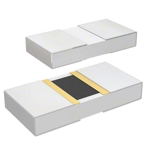
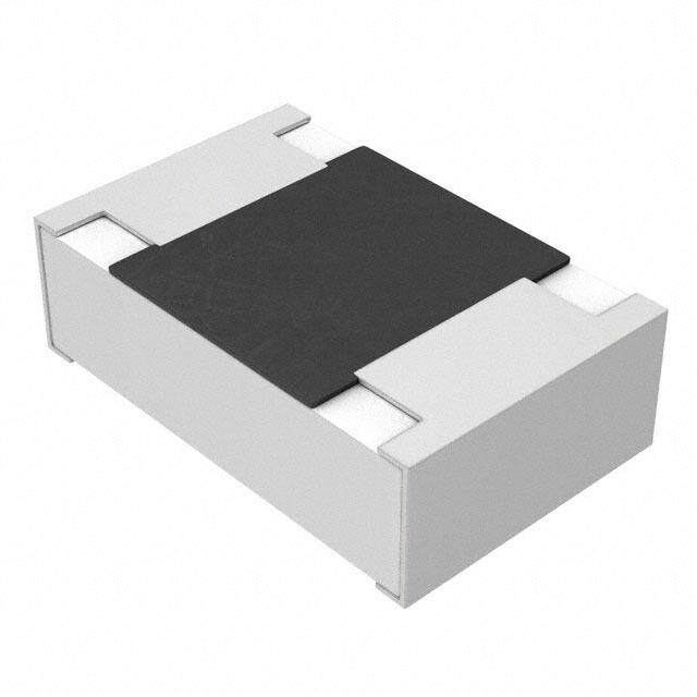
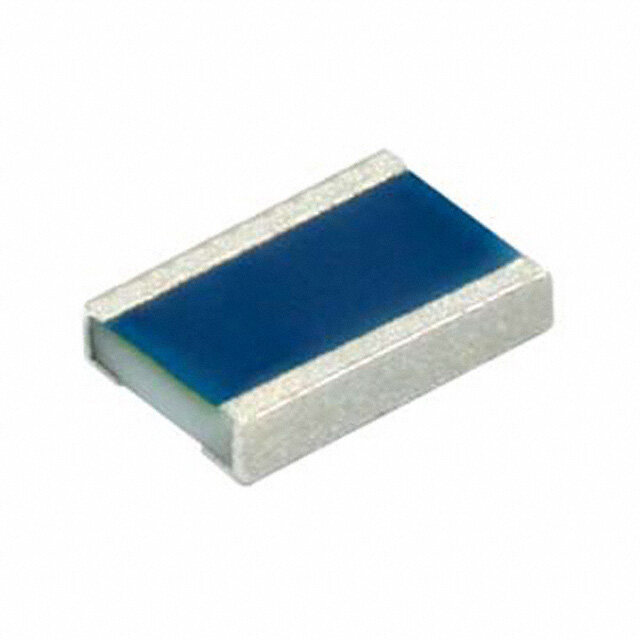
| 描述 | SCR SENS 400V 4A TO252-3SCR 4A 50uA 400V Sensing |
| 产品分类 | SCR - 单个分离式半导体 |
| GateTriggerCurrent-Igt | 50 uA |
| GateTriggerVoltage-Vgt | 0.8 V |
| 品牌 | Littelfuse |
| 产品手册 | |
| 产品图片 |
|
| rohs | 符合RoHS无铅 / 符合限制有害物质指令(RoHS)规范要求 |
| 产品系列 | 晶体闸流管,SCR,Littelfuse S4004DS1RP- |
| 数据手册 | |
| 产品型号 | S4004DS1RP |
| SCR类型 | 灵敏栅极 |
| 不重复通态电流 | 30 A |
| 产品种类 | TVS SCR's |
| 供应商器件封装 | TO-252,(D-Pak) |
| 保持电流Ih最大值 | 4 mA |
| 关闭状态漏泄电流(在VDRMIDRM下) | 0.002 mA |
| 其它名称 | F5664TR |
| 包装 | 带卷 (TR) |
| 商标 | Littelfuse |
| 安装类型 | 表面贴装 |
| 安装风格 | SMD/SMT |
| 封装 | Reel |
| 封装/外壳 | TO-252-3,DPak(2 引线+接片),SC-63 |
| 封装/箱体 | TO-252 |
| 工作温度 | -40°C ~ 110°C |
| 工厂包装数量 | 2500 |
| 开启状态RMS电流-ItRMS | 4 A |
| 最大工作温度 | + 110 C |
| 最大栅极峰值反向电压 | 6 V |
| 最小工作温度 | - 40 C |
| 栅极触发电压-Vgt | 0.8 V |
| 栅极触发电流-Igt | 50 uA |
| 标准包装 | 2,500 |
| 正向电压下降 | 1.6 V |
| 电压-断态 | 400V |
| 电压-栅极触发(Vgt)(最大值) | 800mV |
| 电压-通态(Vtm)(最大值) | 1.6V |
| 电流-不重复浪涌50、60Hz(Itsm) | 25A,30A |
| 电流-保持(Ih)(最大值) | 4mA |
| 电流-断态(最大值) | 2µA |
| 电流-栅极触发(Igt)(最大值) | 50µA |
| 电流-通态(It(AV))(最大值) | 2.5A |
| 电流-通态(It(RMS))(最大值) | 4A |
| 系列 | Sxx04xSx |
| 额定重复关闭状态电压VDRM | 400 V |


PDF Datasheet 数据手册内容提取
Thyristors 4 Amp Sensitive SCRs Sxx04xSx Series RoHS Description Excellent unidirectional switches for phase control applications such as heating and motor speed controls. Sensitive gate SCRs are easily triggered with microAmps of current as furnished by sense coils, proximity switches, and microprocessors. Features & Benefits • RoHS compliant • Voltage capability up to 600 V • Glass – passivated junctions • Surge capability up to 30 A Main Features Applications Typical applications are capacitive discharge systems for Symbol Value Unit strobe lights, nailers, staplers and gas engine ignition. Also I 4 A controls for power tools, home/brown goods and white T(RMS) goods appliances. V /V 400 or 600 V DRM RRM I 50 or 200 μA GT Schematic Symbol Additional Information A K Datasheet Resources Samples G Absolute Maximum Ratings Symbol Parameter Test Conditions Value Unit I RMS on-state current T = 95°C 4 A T(RMS) C I Average on-state current T = 95°C 2.5 A T(AV) C single half cycle; f = 50Hz; 25 T (initial) = 25°C I Peak non-repetitive surge current J A TSM single half cycle; f = 60Hz; 30 T (initial) = 25°C J I2t I2t Value for fusing t = 8.3 ms 3.7 A2s p di/dt Critical rate of rise of on-state current f = 60Hz ; T = 110°C 50 A/μs J I Peak gate current T = 110°C 1 A GM J P Average gate power dissipation T = 110°C 0.1 W G(AV) J T Storage temperature range -40 to 150 °C stg T Operating junction temperature range -40 to 110 °C J © 2018 Littelfuse, Inc. Specifications are subject to change without notice. Revised: 01/16/18
Thyristors 4 Amp Sensitive SCRs Electrical Characteristics — (T = 25°C, unless otherwise specified) J Value Symbol Test Conditions Unit Sxx04xS1 Sxx04xS2 I MAX. 50 200 µA GT V = 6V; R = 100 Ω V D L MAX. 0.8 V GT dv/dt V = V ; R = 1kΩ TYP. 8 V/μs D DRM GK V V = V ; R = 3.3 kΩ; T = 110°C MIN. 0.2 V GD D DRM L J V I = 10µA MIN. 6 V GRM GR I I = 20mA (initial); R = 1kohm MAX. 4 6 mA H T GK t (1) MAX. 50 μs q t I = 2 x I ; PW = 15µs; I = 8A TYP. 3 4 μs gt G GT T Notes : xx = voltage, x = package (1) I=2A; t=50µs; dv/dt=5V/µs; di/dt=-10A/µs T p Static Characteristics Symbol Test Conditions Value Unit V Sxx04xSy I = 8A; t = 380 µs MAX. 1.6 V TM T p T = 25°C 2 I / I V / V - R = 1kohm J MAX. μA DRM RRM DRM RRM GK T = 110°C 100 J Note : xx or z = voltage, x = package, y = sensitivity Thermal Resistances Symbol Parameter Value Unit Sxx04VSy 3.8 R Junction to case (AC) °C/W θ(J-C) Sxx04DSy 3.0 R Junction to ambient Sxx04VSy 85 °C/W θ(J-A) Notes: xx = voltage, y = sensitivity © 2018 Littelfuse, Inc. Specifications are subject to change without notice. Revised: 01/16/18
Thyristors 4 Amp Sensitive SCRs Figure 1: Normalized DC Gate Trigger Current Figure 2: Normalized DC Gate Trigger Voltage vs. Junction Temperature vs. Junction Temperature 4.0 2.0 of I/ I(T = 25°C)GT GTJ23..00 V/ V(T = 25°C)GT GTJ11..05 atio o of R 1.0 ati0.5 R 0.0 0.0 -40 -15 10 35 60 85 110 -40 -15 10 35 60 85 110 Junction Temperature (TJ) -- (°C) Junction Temperature (TJ) -- (°C) Figure 3: Normalized DC Holding Current Figure 4: Normalized DC Latching Current vs. Junction Temperature vs. Junction Temperature 3.0 3.0 2.5 2.5 C) Ratio of I/ I(T= 25°H HJ 112...050 atio of I/ I(T = 25°C)L LJ112...050 R 0.5 0.5 0.0 0.0 -40 -15 10 35 60 85 110 -40 -15 10 35 60 85 110 Junction Temperature (T) -- (°C) Junction Temperature (T) -- (°C) J J Figure 5: On-State Current vs. On-State Figure 6: Power Dissipation (Typical) Voltage (Typical) vs. RMS On-State Current 25 5.5 s nstantaneous On-state Current (i) – AmpT1120505 TJ = 25°C SSxxxx0044VDSSyy Average On-State Power Dissipation [P] - (Watts)D(AV) 0112233445..........5050505050 SSxxxx0044VDSSyy I 0 0.0 0.7 0.8 0.9 1.0 1.1 1.2 1.3 1.4 1.5 1.6 0.0 0.5 1.0 1.5 2.0 2.5 3.0 3.5 4.0 Instantaneous On-state Voltage (v) – Volts RMS On-State Current [IT(RMS)] - (Amps) Note: xx or z = voltage, y = sensitivity © 2018 Littelfuse, Inc. Specifications are subject to change without notice. Revised: 01/16/18
Thyristors 4 Amp Sensitive SCRs Figure 7: Maximum Allowable Case Temperature Figure 8: Maximum Allowable Case Temperature vs. RMS On-State Current vs. Average On-State Current 115 115 110 110 Maximum Allowable Case Temperature (T) - °CC11008899500505 SSxxxx0044VDSSyy Maximum Allowable Case Temperature (T) - °CC11088990050505 SSxxxx0044VDSSyy CURRENT WAVEFORM: Sinusoidal CURRENT WAVEFORM: Sinusoidal 75 LOAD: Resistive or Inductive 75 LOAD: Resistive or Inductive CONDUCTION ANGLE: 180° CONDUCTION ANGLE: 180° 70 70 0.0 0.5 1.0 1.5 2.0 2.5 3.0 3.5 4.0 4.5 0.0 0.5 1.0 1.5 2.0 2.5 3.0 RMS On-State Current [I ] - Amps Average On-State Current [I ] - Amps T(RMS) T(AVE) Figure 9: Maximum Allowable Ambient Temperature Figure 10: Maximum Allowable Ambient Temperature vs. RMS On-State Current vs. Average On-State Current mperature 110200 CLCFORUOEARNEDRD A:EU RNIRCeT TsR WIiOsAtATNivVIN eAE GNFoOrG RILnMEd:u: 1cS8ti0inv°uesoidal ent 110200 CLCFORUOEARNEDRD A:EU RINRCeT TsR WiIsAOtATNivIVN eAE GNoFOrG IRLnMEd:u :1 cS8tii0nv°uesoidal wable Ambient Te(T) -°CA 6800 Sxx04VSy m Allowable Ambiperature (T) -°CA6800 Sxx04VSy m Allo 40 aximuTem40 u M m 20 20 xi a M 0 0 0.0 0.2 0.4 0.6 0.8 1.0 1.2 1.4 0.0 0.2 0.4 0.6 0.8 RMS On-State Current [IT(RMS)] - Amps Average On-State Current [IT(AVE)] - Amps Figure 11: Peak Repetitive Capacitor Discharge Current Figure 12: Peak Repetitive Sinusoidal Pulse Current 180 180 s mp 160 ps 160 A m e Current (I) -TM 111042000 112 HHzz urrent (I ) - ATM 111024000 1 Hz arg 80 60 Hz e C 80 12 Hz h g Peak Disc 4600 ITRM k Dischar 4600 ITM 60 Hz a 20 tW Pe 20 tW 0 0 1 10 100 1 10 100 Pulse Current Duration (tW) - μs Pulse Current Duration (tW) - μs Note: xx = voltage, y = sensitivity © 2018 Littelfuse, Inc. Specifications are subject to change without notice. Revised: 01/16/18
Thyristors 4 Amp Sensitive SCRs Figure 13-1: Typical DC Gate Trigger Current with R Figure 13-2: Typical DC Gate Trigger Current with R GK GK vs. Junction Temperature for S6004xS2 vs. Junction Temperature for S6004xS1 100 R =10Ω GK 10 R =100Ω GK A) m GT ( 1 RGK=470Ω nt I Curre 0.1 RGK=1KΩ er g g Tri 0.01 No RGK 0.001 -40- 15 10 35 60 85 110 Junction Temperature (T J) --(°C) Figure 14-1: Typical DC Holding Current with R Figure 14-2 Typical DC Holding Current with R GK GK vs. Junction Temperature for S6004xS2 vs. Junction Temperature for S6004xS1 Figure 15-1: Typical Static dv/dt with R vs. Junction Figure 15-2 Typical Static dv/dt with R vs. Junction GK GK Temperature for S6004xS2 Temperature for S6004xS1 © 2018 Littelfuse, Inc. Specifications are subject to change without notice. Revised: 01/16/18
Thyristors 4 Amp Sensitive SCRs Figure 16-1: Typical turn off time with R Figure 16-2: Typical turn off time with R GK GK vs. Junction Temperature for S6004xS2 vs. Junction Temperature for S6004xS1 Figure 17: Surge Peak On-State Current vs. Number of Cycles 100.0 SUPPLY FREQUENCY: 60 Hz Sinusoidal Sxx04VSy LOAD: Resistive Sxx04DSy ve)mps RMS On-State Current: [IT(RMS)]: Maximum Rated Peak Surge (Non-repetitiOn-state Current (I) – ATSM101..00 VN12..ao l Gf Otrtuoeaeaevtlmslete o:eadprwt l eco vSiornaaapndgltuet umrsecrou.iefialr yemgh deana soyCc t urab erbserteeeu l nrorTnetse eptimnd edt apetuoterrev irnsdaatg lte.uu aanrndetidyl - jsiumtnamctetei o dnia tely 0.1 1 10 100 1000 Surge Current Duration -- Full Cycles Note: xx or z - voltage, y = sensitivity Figure 18: Simple Test Circuit for Gate Trigger Voltage and Current Reset Note: V1 — 0 V to 10 V dc meter Normally-closed V — 0 V to 1 V dc meter Pushbutton IG —T 0 mA to 1 mA dc milliammeter G R1 — 1 k potentiometer To measure gate trigger voltage and current, raise gate 100 voltage (V ) until meter reading V1 drops from 6 V to 1 V. GT Gate trigger voltage is the reading on V just prior to V1 + GT D.U.T. dropping. Gate trigger current I Can be computed from 6VDC– IGT IN4001 the relationship GT I R1 V1 (11% k) G VGT 100 I = I - _ V__GT_ Amps G T G 1000 where I is reading (in amperes) on meter just prior to V1 G dropping Note: I may turn out to be a negative quantity (trigger GT current flows out from gate lead). If negative current occurs, I value is not a valid reading. Remove 1 k resistor GT and use I as the more correct I value. This will occur on G GT 12 µA gate products. © 2018 Littelfuse, Inc. Specifications are subject to change without notice. Revised: 01/16/18
Thyristors 4 Amp Sensitive SCRs Soldering Parameters Reflow Condition Pb – Free assembly t P T P - Temperature Min (T ) 150°C s(min) e RRaammpp--uupp Pre Heat -- TTeimmep e(mraitnu rteo Mmaaxx )( T(ts()max)) 2600 0–° C180 secs rutare TS(mTaxL) tL s p m RRaammpp--ddoown Average ramp up rate (Liquidus Temp) PPrreehheeaatt 5°C/second max e (TL) to peak T TS(min) t T to T - Ramp-up Rate 5°C/second max S S(max) L - Temperature (T) (Liquidus) 217°C Reflow L 25 - Temperature (t) 60 – 150 seconds time to peak temperature L Time Peak Temperature (T) 260+0/-5 °C P Time within 5°C of actual peak 20 – 40 seconds Temperature (t) p Ramp-down Rate 5°C/second max Time 25°C to peak Temperature (T) 8 minutes Max. P Do not exceed 280°C Physical Specifications Environmental Specifications Test Specifications and Conditions Terminal Finish 100% Matte Tin-plated MIL-STD-750, M-1040, Cond A Applied AC Blocking Peak AC voltage @ 125°C for 1008 hours , Body Material UraLti nregc 9o4gVn-i0zed epoxy meeting flammability RGK = 1kohms MIL-STD-750, M-1051, Temperature Cycling 100 cycles; -40°C to +150°C; Lead Material Copper Alloy 15-min dwell-time EIA / JEDEC, JESD22-A101 Temperature/ 1008 hours; 320V - DC: 85°C; Humidity 85% rel humidity Design Considerations MIL-STD-750, M-1031, High Temp Storage 1008 hours; 150°C Careful selection of the correct component for the application’s operating parameters and environment will Low-Temp Storage 1008 hours; -40°C go a long way toward extending the operating life of the Resistance to Thyristor. Good design practice should limit the maximum MIL-STD-750 Method 2031 Solder Heat continuous current through the main terminals to 75% of the component rating. Other ways to ensure long life for Solderability ANSI/J-STD-002, category 3, Test A a power discrete semiconductor are proper heat sinking Lead Bend MIL-STD-750, M-2036 Cond E and selection of voltage ratings for worst case conditions. Overheating, overvoltage (including dv/dt), and surge currents are the main killers of semiconductors. Correct mounting, soldering, and forming of the leads also help protect against component damage. © 2018 Littelfuse, Inc. Specifications are subject to change without notice. Revised: 01/16/18
Thyristors 4 Amp Sensitive SCRs Dimensions — TO-251AA (V/I-Package) — V/I-PAK Through Hole T MEASURING POINT AREA: 0.040 IN2 Inches Millimeters C Dimension Min Typ Max Min Typ Max Anode E H 5.28 D J .208 A 0.037 0.040 0.043 0.94 1.01 1.09 B 0.235 0.242 0.245 5.97 6.15 6.22 A C 0.350 0.361 0.375 8.89 9.18 9.53 5.34 .210 D 0.205 0.208 0.213 5.21 5.29 5.41 B E 0.255 0.262 0.265 6.48 6.66 6.73 P R F 0.027 0.031 0.033 0.69 0.80 0.84 S Q G 0.087 0.090 0.093 2.21 2.28 2.36 K H 0.085 0.092 0.095 2.16 2.34 2.41 C I 0.176 0.180 0.184 4.47 4.57 4.67 J 0.018 0.020 0.023 0.46 0.51 0.58 K 0.035 0.037 0.039 0.90 0.95 1.00 Cathode F L L 0.018 0.020 0.023 0.46 0.52 0.58 Anode G GATE P 0.042 0.047 0.052 1.06 1.20 1.32 I Q 0.034 0.039 0.044 0.86 1.00 1.11 R 0.034 0.039 0.044 0.86 1.00 1.11 S 0.074 0.079 0.084 1.86 2.00 2.11 Dimensions — TO-252AA (D-Package) — D-PAK Surface Mount Anode DE TC MEASURING POINT .52.0288 .62.6741 Dimension Inches Millimeters Min Typ Max Min Typ Max A 5.34 6.71 A 0.037 0.040 0.043 0.94 1.01 1.09 .210 .264 B B 0.235 0.243 0.245 5.97 6.16 6.22 C 0.106 0.108 0.113 2.69 2.74 2.87 1.60 C QP .063 D 0.205 0.208 0.213 5.21 5.29 5.41 1.80 GATE .071 E 0.255 0.262 0.265 6.48 6.65 6.73 Cathode F AREA: 0.040 IN2 Anode G .1138 .41.8610 F 0.027 0.031 0.033 0.69 0.80 0.84 I G 0.087 0.090 0.093 2.21 2.28 2.36 O L H 0.085 0.092 0.095 2.16 2.33 2.41 K J H I 0.176 0.179 0.184 4.47 4.55 4.67 M J 0.018 0.020 0.023 0.46 0.51 0.58 N K 0.035 0.037 0.039 0.90 0.95 1.00 L 0.018 0.020 0.023 0.46 0.51 0.58 M 0.000 0.000 0.004 0.00 0.00 0.10 N 0.021 0.026 0.027 0.53 0.67 0.69 O 0° 0° 5° 0° 0° 5° P 0.042 0.047 0.052 1.06 1.20 1.32 Q 0.034 0.039 0.044 0.86 1.00 1.11 © 2018 Littelfuse, Inc. Specifications are subject to change without notice. Revised: 01/16/18
Thyristors 4 Amp Sensitive SCRs Product Selector Voltage Part Number Gate Sensitivity Type Package 400V 600V 800V 1000V Sxx04DS1 X X 50μA Sensitive SCR TO-252 Sxx04DS2 X X 200μA Sensitive SCR TO-252 Sxx04VS1 X X 50μA Sensitive SCR TO-251 Sxx04VS2 X X 200μA Sensitive SCR TO-251 Note: xx = Voltage Packing Options Part Number Marking Weight Packing Mode Base Quantity Sxx04DSyTP Sxx04DSy 0.3g Tube 750 (75 per tube) Sxx04DSyRP Sxx04DSy 0.3g Embossed Carrier 2500 Sxx04VSyTP Sxx04VSy 0.4g Tube 750 (75 per tube) Note: xx = voltage, y = sensitivity TO-252 Embossed Carrier Reel Pack (RP) Specs Part Marking System 0(.41.507) Gate 0(1..055)9 DIA Cathode TTOO--225521AAAA-- ((VD PPaacckkaaggee)) L6004V4 L6004V4 (016.6.03) (01.35.234)* XXXXXX XXDC XXXXXX XXDC XXXXXX XXDC XXXXXX YMLDD YMLDD * Cover tape 0.315 Anode ® ® (8.0) Date Code Marking Y:Year Code 12.99 M: Month Code 0.512 (13.0) (330.0) L: Location Code Arbor Hole Dimensions DD: Calendar Code Diameter are in inches (and millimeters). Part Numbering System 0.64 (16.3) S 6004 V S1 Direction of Feed DEVICE TYPE S: SCR SENSITIVITY & TYPE VOLTAGE RATING 4: 400V S1: 50µA 6: 600V S2: 200µA CURRENT RATING PACKAGE TYPE 04: 4A V: TO-251 (V/I-Pak) D: TO-252 (D-Pak) © 2018 Littelfuse, Inc. Specifications are subject to change without notice. Revised: 01/16/18
Mouser Electronics Authorized Distributor Click to View Pricing, Inventory, Delivery & Lifecycle Information: L ittelfuse: T106B11 T107D2 S2004VS2TP S2004DS2TP S4004VS1 S2004DS1TP T106B1 S6004DS1RP S4004VS1TP S6004VS1TP S2004VS1TP S2004VS2 S4004DS1TP T106B1TP T106M1TP T106B41 T106D11 T106D21 T106D41 T106M2 T107D12 T107D21 T106D4 T106D2 S2004VS1 T107D1 S2004DS1RP S2004DS2RP S6004VS1 S4004DS1RP T107M1 S6004DS2RP S4004DS2RP S6004DS1TP S6004VS2TP S4004VS2 S6004DS2TP T107B1 T106D1 T106M1 S4004VS2TP S4004DS2TP S6004VS2