 Datasheet下载
- 型号: S29GL01GS11TFIV10
- 制造商: SPANSION
- 库位|库存: xxxx|xxxx
- 要求:
| 数量阶梯 | 香港交货 | 国内含税 |
| +xxxx | $xxxx | ¥xxxx |
查看当月历史价格
查看今年历史价格
S29GL01GS11TFIV10产品简介:
ICGOO电子元器件商城为您提供S29GL01GS11TFIV10由SPANSION设计生产,在icgoo商城现货销售,并且可以通过原厂、代理商等渠道进行代购。 S29GL01GS11TFIV10价格参考¥73.70-¥96.64。SPANSIONS29GL01GS11TFIV10封装/规格:存储器, FLASH - NOR Memory IC 1Gb (64M x 16) Parallel 110ns 56-TSOP。您可以下载S29GL01GS11TFIV10参考资料、Datasheet数据手册功能说明书,资料中有S29GL01GS11TFIV10 详细功能的应用电路图电压和使用方法及教程。
Cypress Semiconductor Corp的S29GL01GS11TFIV10是一款1Gb(128M x 8/64M x 16)的串行NOR Flash存储器,属于其Gladiator系列,广泛应用于对高可靠性、高性能和宽温工作范围有要求的工业和通信领域。

该器件主要应用场景包括:工业自动化控制系统,如PLC(可编程逻辑控制器)、HMI(人机界面)设备,用于存储固件、配置参数和实时数据;网络与通信设备,如路由器、交换机和基站,支持快速启动和代码执行;汽车电子系统,适用于车载信息娱乐系统和高级驾驶辅助系统(ADAS),具备出色的抗干扰能力和-40°C至+85°C的工业级温度范围;医疗设备中用于存储关键操作程序和校准数据,确保运行稳定与安全;此外,还适用于航空电子、军事和航空航天等高可靠性要求的环境。

S29GL01GS11TFIV10支持多种电压接口(1.7–1.9V核心电压,3.0–3.6V I/O电压),兼容CECC、JEDEC标准,具备高耐用性(典型擦写次数达10万次)和长达20年的数据保持能力。其封装形式为64-ball FBGA,体积小,适合空间受限的高密度电路板设计。通过支持同步和异步两种读取模式,提升了系统灵活性和访问效率。

综上,该型号适用于需要大容量、高稳定性、长期供货保障的嵌入式系统,是工业、通信、汽车及高端消费类电子中的理想非易失性存储解决方案。
| 参数 | 数值 |
| 品牌 | Spansion |
| 产品目录 | 半导体 |
| 描述 | 闪存 1G 3V 110ns Parallel NOR 闪存 |
| 产品分类 | 集成电路 - IC |
| 产品手册 | |
| 产品图片 |
|
| rohs | 符合RoHS |
| 产品系列 | 内存,闪存,Spansion S29GL01GS11TFIV10 |
| 产品型号 | S29GL01GS11TFIV10 |
| 产品种类 | 闪存 |
| 商标 | Spansion |
| 存储容量 | 1 Gbit |
| 存储类型 | NOR |
| 安装风格 | SMD/SMT |
| 定时类型 | Asynchronous |
| 封装 | Tray |
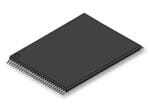
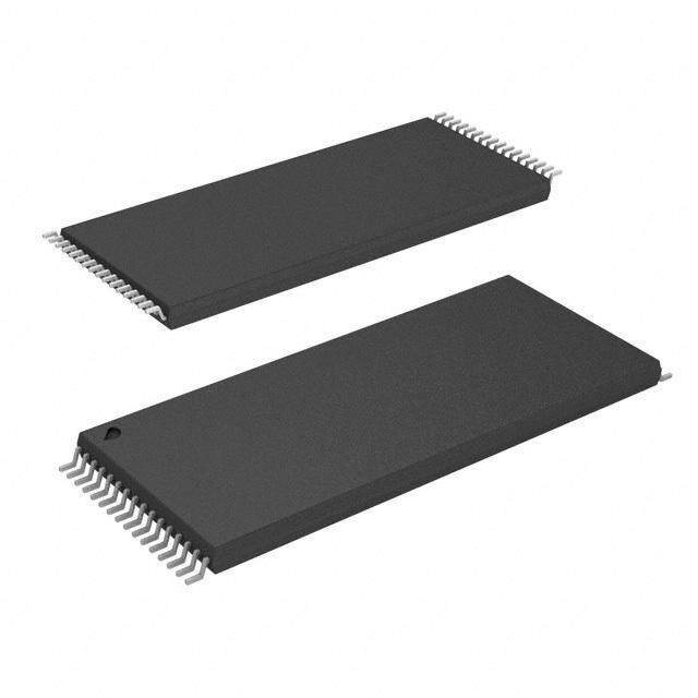
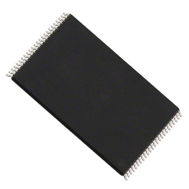
| 封装/箱体 | TSOP-56 |
| 工作温度 | - 40 C to + 85 C |
| 工作温度范围 | - 40 C to + 85 C |
| 工厂包装数量 | 91 |
| 接口类型 | Parallel |
| 数据总线宽度 | 16 bit |
| 最大工作电流 | 100 mA |
| 电源电压-最大 | 3.6 V |
| 电源电压-最小 | 2.7 V |
| 系列 | S29GL01GS |
| 组织 | 64 M x 16 |
| 结构 | Eclipse |
| 访问时间 | 15 ns |
| 速度 | 110 ns |


- 商务部:美国ITC正式对集成电路等产品启动337调查
- 曝三星4nm工艺存在良率问题 高通将骁龙8 Gen1或转产台积电
- 太阳诱电将投资9.5亿元在常州建新厂生产MLCC 预计2023年完工
- 英特尔发布欧洲新工厂建设计划 深化IDM 2.0 战略
- 台积电先进制程称霸业界 有大客户加持明年业绩稳了
- 达到5530亿美元!SIA预计今年全球半导体销售额将创下新高
- 英特尔拟将自动驾驶子公司Mobileye上市 估值或超500亿美元
- 三星加码芯片和SET,合并消费电子和移动部门,撤换高东真等 CEO
- 三星电子宣布重大人事变动 还合并消费电子和移动部门
- 海关总署:前11个月进口集成电路产品价值2.52万亿元 增长14.8%


PDF Datasheet 数据手册内容提取
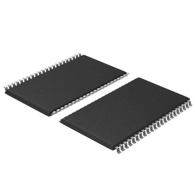
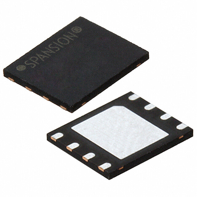
S29GL01GS/S29GL512S S29GL256S/S29GL128S 1-Gbit (128 Mbyte)/512-Mbit (64 Mbyte)/ 256-Mbit (32 Mbyte)/128-Mbit (16 Mbyte), 3.0 V, GL-S Flash Memory General Description The Cypress® S29GL01G/512/256/128S are MirrorBit® Eclipse flash products fabricated on 65 nm process technology. These devices offer a fast page access time as fast as 15ns with a corresponding random access time as fast as 90ns. They feature a Write Buffer that allows a maximum of 256 words/512 bytes to be programmed in one operation, resulting in faster effective programming time than standard programming algorithms. This makes these devices ideal for today’s embedded applications that require higher density, better performance and lower power consumption. Distinctive Characteristics CMOS 3.0 Volt Core with Versatile I/O Status Register, Data Polling, and Ready/Busy pin methods 65 nm MirrorBit Eclipse Technology to determine device status Single supply (V ) for read / program / erase (2.7 V to Advanced Sector Protection (ASP) CC 3.6V) –Volatile and non-volatile protection methods for each Versatile I/O Feature sector –Wide I/O voltage range (V ): 1.65 V to V Separate 1024-byte One Time Program (OTP) array with two IO CC lockable regions ×16 data bus Common Flash Interface (CFI) parameter table Asynchronous 32-byte Page read Temperature Range / Grade 512-byte Programming Buffer –Industrial (-40 °C to +85 °C) –Programming in Page multiples, up to a maximum of 512bytes –Industrial Plus(-40 °C to +105 °C) –Automotive, AEC-Q100 Grade 3 (-40 °C to +85 °C) Single word and multiple program on same word options –Automotive, AEC-Q100 Grade 2 (-40 °C to +105 °C) Automatic Error Checking and Correction (ECC) – internal hardware ECC with single bit error correction 100,000 Program / Erase Cycles Sector Erase 20 Years Data Retention –Uniform 128-kbyte sectors Packaging Options Suspend and Resume commands for Program and Erase –56-pin TSOP operations –64-ball LAA Fortified BGA, 13 mm × 11 mm –64-ball LAE Fortified BGA, 9 mm × 9 mm –56-ball VBU Fortified BGA, 9 mm × 7 mm CypressSemiconductorCorporation • 198 Champion Court • SanJose, CA 95134-1709 • 408-943-2600 Document Number: 001-98285 Rev. *R Revised June 21, 2018
S29GL01GS/S29GL512S S29GL256S/S29GL128S Performance Summary Maximum Read Access Times Random Access Page Access Time CE# Access Time OE# Access Time Density Voltage Range Time (t ) (t ) (t ) (t ) ACC PACC CE OE Full V = V 90 15 90 25 CC IO 128 Mb VersatileIO V 100 25 100 35 IO Full V = V 90 15 90 25 CC IO 256 Mb VersatileIO V 100 25 100 35 IO Full V = V 100 15 100 25 CC IO 512 Mb VersatileIO V 110 25 110 35 IO Full V = V 100 15 100 25 CC IO 1 Gb VersatileIO V 110 25 110 35 IO Typical Program and Erase Rates Buffer Programming 1.5 MB/s (512 bytes) Sector Erase (128 kbytes) 477 kB/s Maximum Current Consumption Active Read at 5 MHz, 30 pF 60 mA Program 100 mA Erase 100 mA Standby 100 µA Document Number: 001-98285 Rev. *R Page 3 of 108
S29GL01GS/S29GL512S S29GL256S/S29GL128S Contents General Description............................................................. 2 9.4 Read............................................................................. 67 9.5 Write............................................................................. 68 Distinctive Characteristics.................................................. 2 10. Electrical Specifications............................................. 69 Performance Summary........................................................ 3 10.1 Absolute Maximum Ratings.......................................... 69 1. Product Overview........................................................ 4 10.2 Latchup Characteristics................................................ 69 10.3 Thermal Resistance...................................................... 69 2. Address Space Maps................................................... 6 10.4 Operating Ranges......................................................... 69 2.1 Flash Memory Array....................................................... 7 10.5 DC Characteristics........................................................ 72 2.2 Device ID and CFI (ID-CFI) ASO................................... 8 10.6 Capacitance Characteristics......................................... 74 2.3 Device ID and Common Flash Interface (ID-CFI) ASO Map — Automotive Only....................................... 9 11. Timing Specifications................................................. 75 2.4 Status Register ASO.................................................... 10 11.1 Key to Switching Waveforms........................................ 75 2.5 Data Polling Status ASO.............................................. 10 11.2 AC Test Conditions....................................................... 75 2.6 Secure Silicon Region ASO......................................... 10 11.3 Power-On Reset (POR) and Warm Reset.................... 76 2.7 Sector Protection Control............................................. 11 11.4 AC Characteristics........................................................ 78 2.8 ECC Status ASO.......................................................... 11 12. Physical Interface....................................................... 90 3. Data Protection.......................................................... 13 12.1 56-pin TSOP................................................................. 90 3.1 Device Protection Methods.......................................... 13 12.2 64-Ball FBGA................................................................ 92 3.2 Command Protection................................................... 13 12.3 56-Ball FBGA................................................................ 95 3.3 Secure Silicon Region (OTP)....................................... 13 13. Special Handling Instructions 3.4 Sector Protection Methods........................................... 14 for FBGA Package...................................................... 96 4. Read Operations........................................................ 19 14. Ordering Information.................................................. 97 4.1 Asynchronous Read..................................................... 19 4.2 Page Mode Read......................................................... 19 15. Other Resources....................................................... 102 15.1 Cypress Flash Memory Roadmap.............................. 102 5. Embedded Operations............................................... 20 15.2 Links to Software........................................................ 102 5.1 Embedded Algorithm Controller (EAC)........................ 20 15.3 Links to Application Notes........................................... 102 5.2 Program and Erase Summary..................................... 21 5.3 Automatic ECC............................................................ 22 16. Revision History........................................................ 103 5.4 Command Set.............................................................. 23 5.5 Status Monitoring......................................................... 34 5.6 Error Types and Clearing Procedures......................... 40 5.7 Embedded Algorithm Performance Table.................... 43 6. Data Integrity.............................................................. 54 6.1 Erase Endurance......................................................... 54 6.2 Data Retention............................................................. 54 7. Software Interface Reference................................... 55 7.1 Command Summary.................................................... 55 7.2 Device ID and Common Flash Interface (ID-CFI) ASO Map..................................................................... 58 7.3 Device ID and Common Flash Interface (ID-CFI) ASO Map..................................................................... 63 8. Signal Descriptions................................................... 64 8.1 Address and Data Configuration.................................. 64 8.2 Input/Output Summary................................................. 64 8.3 Versatile I/O Feature.................................................... 65 8.4 Ready/Busy# (RY/BY#)............................................... 65 8.5 Hardware Reset........................................................... 65 9. Signal Protocols......................................................... 66 9.1 Interface States............................................................ 66 9.2 Power-Off with Hardware Data Protection................... 66 9.3 Power Conservation Modes......................................... 67 Document Number: 001-98285 Rev. *R Page 3 of 108
S29GL01GS/S29GL512S S29GL256S/S29GL128S 1. Product Overview The GL-S family consists of 128-Mbit to 1Gbit, 3.0 V core, Versatile I/O, non-volatile, flash memory devices. These devices have a 16-bit (word) wide data bus and use only word boundary addresses. All read accesses provide 16 bits of data on each bus transfer cycle. All writes take 16 bits of data from each bus transfer cycle. Figure 1.1 Block Diagram RY/BY# DQ15–DQ0 VCC Sector Switches VSS V IO Erase Voltage Input/Output Generator Buffers RESET# WE# State WP# Control Command Register PGM Voltage Generator Chip Enable Data CE# Output Enable STB Latch Logic OE# Y-Decoder Y-Gating STB VCC Detector Timer h c at L s X-Decoder Cell Matrix s e dr d A AMax**–A0 :Note: ** AMAX GL01GS = A25, AMAX GL512S = A24, AMAX GL256S = A23, AMAX GL128S = A22 The GL-S family combines the best features of eXecute In Place (XIP) and Data Storage flash memories. This family has the fast random access of XIP flash along with the high density and fast program speed of Data Storage flash. Read access to any random location takes 90 ns to 120 ns depending on device density and I/O power supply voltage. Each random (initial) access reads an entire 32-byte aligned group of data called a Page. Other words within the same Page may be read by changing only the low order 4 bits of word address. Each access within the same Page takes 15 ns to 30 ns. This is called Page Mode read. Changing any of the higher word address bits will select a different Page and begin a new initial access. All read accesses are asynchronous. Document Number: 001-98285 Rev. *R Page 4 of 108
S29GL01GS/S29GL512S S29GL256S/S29GL128S Table 1.1 S29GL-S Address Map Type Count Addresses Address within Page 16 A3–A0 Address within Write Buffer 256 A7–A0 Page 4096 A15–A4 Write-Buffer-Line 256 A15–A8 1024 (1 Gb) 512 (512 Mb) Sector A –A16 256 (256 Mb) MAX 128 (128 Mb) The device control logic is subdivided into two parallel operating sections, the Host Interface Controller (HIC) and the Embedded Algorithm Controller (EAC). HIC monitors signal levels on the device inputs and drives outputs as needed to complete read and write data transfers with the host system. HIC delivers data from the currently entered address map on read transfers; places write transfer address and data information into the EAC command memory; notifies the EAC of power transition, hardware reset, and write transfers. The EAC looks in the command memory, after a write transfer, for legal command sequences and performs the related Embedded Algorithms. Changing the non-volatile data in the memory array requires a complex sequence of operations that are called Embedded Algorithms (EA). The algorithms are managed entirely by the device internal EAC. The main algorithms perform programming and erase of the main array data. The host system writes command codes to the flash device address space. The EAC receives the commands, performs all the necessary steps to complete the command, and provides status information during the progress of an EA. The erased state of each memory bit is a logic 1. Programming changes a logic 1 (High) to a logic 0 (Low). Only an Erase operation is able to change a 0 to a 1. An erase operation must be performed on an entire 128-kbyte aligned and length group of data call a Sector. When shipped from Cypress all Sectors are erased. Programming is done via a 512-byte Write Buffer. It is possible to write from 1 to 256 words, anywhere within the Write Buffer before starting a programming operation. Within the flash memory array, each 512-byte aligned group of 512 bytes is called a Line. A programming operation transfers volatile data from the Write Buffer to a non-volatile memory array Line. The operation is called Write Buffer Programming. As the device transfers each 32-byte aligned page of data that was loaded into the Write buffer to the 512-byte Flash array line, internal logic programs an ECC Code for the Page into a portion of the memory array not visible to the host system software. The internal logic checks the ECC information during the initial access of every array read operation. If needed, the ECC information corrects a one bit error during the initial access time. The Write Buffer is filled with 1’s after reset or the completion of any operation using the Write Buffer. Any locations not written to a 0 by a Write to Buffer command are by default still filled with 1’s. Any 1’s in the Write Buffer do not affect data in the memory array during a programming operation. As each Page of data that was loaded into the Write Buffer is transferred to a memory array Line. Sectors may be individually protected from program and erase operations by the Advanced Sector Protection (ASP) feature set. ASP provides several, hardware and software controlled, volatile and non-volatile, methods to select which sectors are protected from program and erase operations. Document Number: 001-98285 Rev. *R Page 5 of 108
S29GL01GS/S29GL512S S29GL256S/S29GL128S Software Interface 2. Address Space Maps There are several separate address spaces that may appear within the address range of the flash memory device. One address space is visible (entered) at any given time. Flash Memory Array: the main non-volatile memory array used for storage of data that may be randomly accessed by asynchronous read operations. ID/CFI: a memory array used for Cypress factory programmed device characteristics information. This area contains the Device Identification (ID) and Common Flash Interface (CFI) information tables. Secure Silicon Region (SSR): a One Time Programmable (OTP) non-volatile memory array used for Cypress factory programmed permanent data, and customer programmable permanent data. Lock Register: an OTP non-volatile word used to configure the ASP features and lock the SSR. Persistent Protection Bits (PPB): a non-volatile flash memory array with one bit for each Sector. When programmed, each bit protects the related Sector from erasure and programming. PPB Lock: a volatile register bit used to enable or disable programming and erasure of the PPB bits. Password: an OTP non-volatile array used to store a 64-bit password used to enable changing the state of the PPB Lock Bit when using Password Mode sector protection. Dynamic Protection Bits (DYB): a volatile array with one bit for each Sector. When set, each bit protects the related Sector from erasure and programming. Status Register: a volatile register used to display Embedded Algorithm status. Data Polling Status: a volatile register used as an alternate, legacy software compatible, way to display Embedded Algorithm status. ECC Status: provides the status of any error detection or correction action taken when reading the selected Page. The main Flash Memory Array is the primary and default address space but, it may be overlaid by one other address space, at any one time. Each alternate address space is called an Address Space Overlay (ASO). Each ASO replaces (overlays) the entire flash device address range. Any address range not defined by a particular ASO address map, is reserved for future use. All read accesses outside of an ASO address map returns non-valid (undefined) data. The locations will display actively driven data but the meaning of whatever 1’s or 0’s appear are not defined. There are four device operating modes that determine what appears in the flash device address space at any given time: Read Mode Data Polling Mode Status Register (SR) Mode Address Space Overlay (ASO) Mode In Read Mode the entire Flash Memory Array may be directly read by the host system memory controller. The memory device Embedded Algorithm Controller (EAC), puts the device in Read mode during Power-on, after a Hardware Reset, after a Command Reset, or after an Embedded Algorithm (EA) is suspended. Read accesses and command writes are accepted in read mode. A subset of commands are accepted in read mode when an EA is suspended. While in any mode, the Status Register read command may be issued to cause the Status Register ASO to appear at every word address in the device address space. In this Status Register ASO Mode, the device interface waits for a read access and, any write access is ignored. The next read access to the device accesses the content of the status register, exits the Status Register ASO, and returns to the previous (calling) mode in which the Status Register read command was received. In EA mode the EAC is performing an Embedded Algorithm, such as programming or erasing a non-volatile memory array. While in EA mode, none of the main Flash Memory Array is readable because the entire flash device address space is replaced by the Data Polling Status ASO. Data Polling Status will appear at every word location in the device address space. Document Number: 001-98285 Rev. *R Page 6 of 108
S29GL01GS/S29GL512S S29GL256S/S29GL128S While in EA mode, only a Program / Erase suspend command or the Status Register Read command will be accepted. All other commands are ignored. Thus, no other ASO may be entered from the EA mode. When an Embedded Algorithm is suspended, the Data Polling ASO is visible until the device has suspended the EA. When the EA is suspended the Data Polling ASO is exited and Flash Array data is available. The Data Polling ASO is reentered when the suspended EA is resumed, until the EA is again suspended or finished. When an Embedded Algorithm is completed, the Data Polling ASO is exited and the device goes to the previous (calling) mode (from which the Embedded Algorithm was started). In ASO mode, one of the remaining overlay address spaces is entered (overlaid on the main Flash Array address map). Only one ASO may be entered at any one time. Commands to the device affect the currently entered ASO. Only certain commands are valid for each ASO. These are listed in the Table7.1 onpage55, in each ASO related section of the table. The following ASOs have non-volatile data that may be programmed to change 1’s to 0’s: Secure Silicon Region Lock Register Persistent Protection Bits (PPB) Password Only the PPB ASO has non-volatile data that may be erased to change 0’s to 1’s When a program or erase command is issued while one of the non-volatile ASOs is entered, the EA operates on the ASO. The ASO is not readable while the EA is active. When the EA is completed the ASO remains entered and is again readable. Suspend and Resume commands are ignored during an EA operating on any of these ASOs. 2.1 Flash Memory Array The S29GL-S family has uniform sector architecture with a sector size of 128 kB. Table2.1 to Table2.4 shows the sector architecture of the four devices. Table 2.1 S29GL01GS Sector and Memory Address Map Address Range Sector Size (kbyte) Sector Count Sector Range Notes (16-Bit) SA00 0000000h–000FFFFh Sector Starting Address 128 1024 : : – SA1023 3FF0000h–3FFFFFFh Sector Ending Address Table 2.2 S29GL512S Sector and Memory Address Map Address Range Sector Size (kbyte) Sector Count Sector Range Notes (16-Bit) SA00 0000000h–000FFFFh Sector Starting Address 128 512 : : – SA511 1FF0000h–1FFFFFFh Sector Ending Address Table 2.3 S29GL256S Sector and Memory Address Map Address Range Sector Size (kbyte) Sector Count Sector Range Notes (16-Bit) SA00 0000000h–000FFFFh Sector Starting Address 128 256 : : – SA255 0FF0000h–0FFFFFFh Sector Ending Address Document Number: 001-98285 Rev. *R Page 7 of 108
S29GL01GS/S29GL512S S29GL256S/S29GL128S Table 2.4 S29GL128S Sector and Memory Address Map Address Range Sector Size (kbyte) Sector Count Sector Range Notes (16-Bit) SA00 0000000h–000FFFFh Sector Starting Address 128 128 : : – SA127 07F0000h–07FFFFFh Sector Ending Address Note: These tables have been condensed to show sector related information for an entire device on a single page Sectors and their address ranges that are not explicitly listed (such as SA001-SA510) have sectors starting and ending addresses that form the same pattern as all other sectors of that size. For example, all 128 kB sectors have the pattern XXX0000h–XXXFFFFh. 2.2 Device ID and CFI (ID-CFI) ASO There are two traditional methods for systems to identify the type of flash memory installed in the system. One has traditionally been called Autoselect and is now referred to as Device Identification (ID). The other method is called Common Flash Interface (CFI). For ID, a command is used to enable an address space overlay where up to 16 word locations can be read to get JEDEC manufacturer identification (ID), device ID, and some configuration and protection status information from the flash memory. The system can use the manufacturer and device IDs to select the appropriate driver software to use with the flash device. CFI also uses a command to enable an address space overlay where an extendable table of standard information about how the flash memory is organized and operates can be read. With this method the driver software does not have to be written with the specifics of each possible memory device in mind. Instead the driver software is written in a more general way to handle many different devices but adjusts the driver behavior based on the information in the CFI table. Traditionally these two address spaces have used separate commands and were separate overlays. However, the mapping of these two address spaces are non-overlapping and so can be combined in to a single address space and appear together in a single overlay. Either of the traditional commands used to access (enter) the Autoselect (ID) or CFI overlay will cause the now combined ID-CFI address map to appear. The ID-CFI address map appears within, and overlays the Flash Array data of, the sector selected by the address used in the ID-CFI enter command. While the ID-CFI ASO is entered the content of all other sectors is undefined. The ID-CFI address map starts at location 0 of the selected sector. Locations above the maximum defined address of the ID-CFI ASO to the maximum address of the selected sector have undefined data. The ID-CFI enter commands use the same address and data values used on previous generation memories to access the JEDEC Manufacturer ID (Autoselect) and Common Flash Interface (CFI) information, respectively. See Figure11.16 onpage87 for ASO Entry timing requirements. Table 2.5 ID-CFI Address Map Overview Word Address Description Read / Write Device ID (SA) + 0000h to 000Fh Read Only (traditional Autoselect values) (SA) + 0010h to 0079h CFI data structure Read Only (SA) + 0080h to FFFFh Undefined Read Only For the complete address map see Table7.2 onpage58. Document Number: 001-98285 Rev. *R Page 8 of 108
S29GL01GS/S29GL512S S29GL256S/S29GL128S 2.3 Device ID and Common Flash Interface (ID-CFI) ASO Map — Automotive Only Example of Hex Read Out of Example Word Address Data Field # of bytes Data Format Actual Data Data Size of Electronic (SA) + 0080h 1 Hex 19 0013h Marking Revision of Electronic (SA) + 0081h 1 Hex 1 0001h Marking 004Ch, 0044h, 0038h, 0037h, (SA) + 0082h Fab Lot # 7 Ascii LD87270 0032h, 0037h, 0030h (SA) + 0089h Wafer # 1 Hex 23 0017h (SA) + 008Ah Die X Coordinate 1 Hex 10 000Ah (SA) + 008Bh Die Y Coordinate 1 Hex 15 000Fh 0042h, 0052h, 0033h, 0033h, (SA) + 008Ch Class Lot # 7 Ascii BR33150 0031h, 0035h, 0030h (SA) + 0093h Reserved for Future 13 n/a n/a undefined Fab Lot # + Wafer # + Die X Coordinate + Die Y Coordinate gives a unique ID for each device. 2.3.1 Device ID The Joint Electron Device Engineering Council (JEDEC) standard JEP106T defines the manufacturer ID for a compliant memory. Common industry usage defined a method and format for reading the manufacturer ID and a device specific ID from a memory device. The manufacturer and device ID information is primarily intended for programming equipment to automatically match a device with the corresponding programming algorithm. Cypress has added additional fields within this 32-byte address space. The original industry format was structured to work with any memory data bus width e. g. ×8, ×16, ×32. The ID code values are traditionally byte wide but are located at bus width address boundaries such that incrementing the device address inputs will read successive byte, word, or double word locations with the ID codes always located in the least significant byte location of the data bus. Because the device data bus is word wide each code byte is located in the lower half of each word location. The original industry format made the high order byte always 0. Cypress has modified the format to use both bytes in some words of the address space. For the detail description of the Device ID address map see Table7.2 onpage58. 2.3.2 Common Flash Memory Interface The JEDEC Common Flash Interface (CFI) specification (JESD68.01) defines a standardized data structure that may be read from a flash memory device, which allows vendor-specified software algorithms to be used for entire families of devices. The data structure contains information for system configuration such as various electrical and timing parameters, and special functions supported by the device. Software support can then be device-independent, Device ID-independent, and forward-and-backward-compatible for entire Flash device families. The system can read CFI information at the addresses within the selected sector as shown in Device ID and Common Flash Interface (ID-CFI) ASO Map onpage58. Like the Device ID information, CFI information is structured to work with any memory data bus width e. g. ×8, ×16, ×32. The code values are always byte wide but are located at data bus width address boundaries such that incrementing the device address reads successive byte, word, or double word locations with the codes always located in the least significant byte location of the data bus. Because the data bus is word wide each code byte is located in the lower half of each word location and the high order byte is always 0. For further information, please refer to the Cypress CFI Specification, Version 1.4 (or later), and the JEDEC publications JEP137-A and JESD68.01. Please contact JEDEC (http://www.jedec.org) for their standards and the Cypress CFI Specification may be found at the Cypress Website (http://www.cypress.com/cypressappnotes) at the time of this document’s publication), or contact the local Cypress sales office listed in the website. Document Number: 001-98285 Rev. *R Page 9 of 108
S29GL01GS/S29GL512S S29GL256S/S29GL128S 2.4 Status Register ASO The Status Register ASO contains a single word of registered volatile status for Embedded Algorithms. When the Status Register read command is issued, the current status is captured (by the rising edge of WE#) into the register and the ASO is entered. The Status Register content appears on all word locations. The first read access exits the Status Register ASO (with the rising edge of CE# or OE#) and returns to the address space map in use when the Status Register read command was issued. Write commands will not exit the Status Register ASO state. 2.5 Data Polling Status ASO The Data Polling Status ASO contains a single word of volatile memory indicating the progress of an EA. The Data Polling Status ASO is entered immediately following the last write cycle of any command sequence that initiates an EA. Commands that initiate an EA are: Word Program Program Buffer to Flash Chip Erase Sector Erase Erase Resume / Program Resume Program Resume Enhanced Method Blank Check Lock Register Program Password Program PPB Program All PPB Erase Engineering Note: The reset and write buffer abort reset commands require very short time to execute so data polling is not supported for these commands.The Data Polling Status word appears at all word locations in the device address space. When an EA is completed the Data Polling Status ASO is exited and the device address space returns to the address map mode where the EA was started. 2.6 Secure Silicon Region ASO The Secure Silicon Region (SSR) provides an extra flash memory area that can be programmed once and permanently protected from further changes i. e. it is a One Time Program (OTP) area. The SSR is 1024 bytes in length. It consists of 512 bytes for Factory Locked Secure Silicon Region and 512 bytes for Customer Locked Secure Silicon Region. The sector address supplied during the Secure Silicon Entry command selects the Flash Memory Array sector that is overlaid by the Secure Silicon Region address map. See Figure11.16 onpage87 for ASO Entry timing requirements. The SSR is overlaid starting at location 0 in the selected sector. Use of the sector 0 address is recommended for future compatibility. While the SSR ASO is entered the content of all other sectors is undefined. Locations above the maximum defined address of the SSR ASO to the maximum address of the selected sector have undefined data. Table 2.6 Secure Silicon Region Word Address Range Content Size (SA) + 0000h to 00FFh Factory Locked Secure Silicon Region 512 bytes (SA) + 0100h to 01FFh Customer Locked Secure Silicon Region 512 bytes (SA) + 0200h to FFFFh Undefined 127 kbytes Document Number: 001-98285 Rev. *R Page 10 of 108
S29GL01GS/S29GL512S S29GL256S/S29GL128S 2.7 Sector Protection Control 2.7.1 Lock Register ASO The Lock register ASO contains a single word of OTP memory. When the ASO is entered the Lock Register appears at all word locations in the device address space. See Figure11.16 onpage87 for ASO Entry timing requirements. However, it is recommended to read or program the Lock Register only at location 0 of the device address space for future compatibility. 2.7.2 Persistent Protection Bits (PPB) ASO The PPB ASO contains one bit of a Flash Memory Array for each Sector in the device. When the PPB ASO is entered, the PPB bit for a sector appears in the Least Significant Bit (LSB) of each address in the sector. See Figure11.16 onpage87 for ASO Entry timing requirements. Reading any address in a sector displays data where the LSB indicates the non-volatile protection status for that sector. However, it is recommended to read or program the PPB only at address 0 of the sector for future compatibility. If the bit is 0 the sector is protected against programming and erase operations. If the bit is 1 the sector is not protected by the PPB. The sector may be protected by other features of ASP. 2.7.3 PPB LOCK ASO The PPB Lock ASO contains a single bit of volatile memory. The bit controls whether the bits in the PPB ASO may be programmed or erased. If the bit is 0 the PPB ASO is protected against programming and erase operations. If the bit is 1 the PPB ASO is not protected. When the PPB Lock ASO is entered the PPB Lock bit appears in the Least Significant Bit (LSB) of each address in the device address space. See Figure11.16 onpage87 for ASO Entry timing requirements. However, it is recommended to read or program the PPB Lock only at address 0 of the device for future compatibility. 2.7.4 Password ASO The Password ASO contains four words of OTP memory. When the ASO is entered the Password appears starting at address 0 in the device address space. See Figure11.16 onpage87 for ASO Entry timing requirements. All locations above the forth word are undefined. 2.7.5 Dynamic Protection Bits (DYB) ASO The DYB ASO contains one bit of a volatile memory array for each Sector in the device. When the DYB ASO is entered, the DYB bit for a sector appears in the Least Significant Bit (LSB) of each address in the sector. See Figure11.16 onpage87 for ASO Entry timing requirements. Reading any address in a sector displays data where the LSB indicates the non-volatile protection status for that sector. However, it is recommended to read, set, or clear the DYB only at address 0 of the sector for future compatibility. If the bit is 0 the sector is protected against programming and erase operations. If the bit is 1 the sector is not protected by the DYB. The sector may be protected by other features of ASP. 2.8 ECC Status ASO The system can access the ECC Status ASO by issuing the ECC Status entry command sequence during Read Mode. The ECC Status ASO provides the status of a Single Bit Error correction when reading the selected page. Automatic ECC onpage22 describes the ECC function in more detail. See Figure11.16 onpage87 for ASO Entry timing requirements. The ECC Status ASO allows the following activities: Read ECC Status for the selected page. ASO Exit. 2.8.1 ECC Status The contents of the ECC Status ASO indicates, for the selected ECC page, whether ECC protection has corrected an error in the eight-bit error correction code or the 16 Words of data in the ECC page. The address specified in the ECC Status Read Command, provided in Table7.1 onpage55 selects the ECC Page. Document Number: 001-98285 Rev. *R Page 11 of 108
S29GL01GS/S29GL512S S29GL256S/S29GL128S Table 2.7 ECC Status Word – Upper Byte Bit 15 14 13 12 11 10 9 8 Name RFU RFU RFU RFU RFU RFU RFU RFU Value X X X X X X X X Table 2.8 ECC Status Word – Lower Byte Bit 7 6 5 4 3 2 1 0 Single Bit Error corrected in the 8-bit Single Bit Error corrected in Name RFU RFU RFU RFU RFU RFU error correction code 16words of data 0 = No Error Corrected 0 = No Error Corrected Value X X X X X X 1 = Single Bit Error Corrected 1 = Single Bit Error Corrected Document Number: 001-98285 Rev. *R Page 12 of 108
S29GL01GS/S29GL512S S29GL256S/S29GL128S 3. Data Protection The device offers several features to prevent malicious or accidental modification of any sector via hardware means. 3.1 Device Protection Methods 3.1.1 Power-Up Write Inhibit RESET#, CE#, WE#, and, OE# are ignored during Power-On Reset (POR). During POR, the device can not be selected, will not accept commands on the rising edge of WE#, and does not drive outputs. The Host Interface Controller (HIC) and Embedded Algorithm Controller (EAC) are reset to their standby states, ready for reading array data, during POR. CE# or OE# must go to V IH before the end of POR (t ). VCS At the end of POR the device conditions are: all internal configuration information is loaded, the device is in read mode, the Status Register is at default value, all bits in the DYB ASO are set to un-protect all sectors, the Write Buffer is loaded with all 1’s, the EAC is in the standby state. 3.1.2 Low V Write Inhibit CC When V is less than V , the HIC does not accept any write cycles and the EAC resets. This protects data during V power-up CC LKO CC and power-down. The system must provide the proper signals to the control pins to prevent unintentional writes when V is greater CC than V . LKO 3.2 Command Protection Embedded Algorithms are initiated by writing command sequences into the EAC command memory. The command memory array is not readable by the host system and has no ASO. Each host interface write is a command or part of a command sequence to the device. The EAC examines the address and data in each write transfer to determine if the write is part of a legal command sequence. When a legal command sequence is complete the EAC will initiate the appropriate EA. Writing incorrect address or data values, or writing them in an improper sequence, will generally result in the EAC returning to its Standby state. However, such an improper command sequence may place the device in an unknown state, in which case the system must write the reset command, or possibly provide a hardware reset by driving the RESET# signal Low, to return the EAC to its Standby state, ready for random read. The address provided in each write may contain a bit pattern used to help identify the write as a command to the device. The upper portion of the address may also select the sector address on which the command operation is to be performed. The Sector Address (SA) includes A through A16 flash address bits (system byte address signals a through a17). A command bit pattern is located MAX max in A10 to A0 flash address bits (system byte address signals a11 through a1). The data in each write may be: a bit pattern used to help identify the write as a command, a code that identifies the command operation to be performed, or supply information needed to perform the operation. See Table7.1 onpage55 for a listing of all commands accepted by the device. 3.3 Secure Silicon Region (OTP) The Secure Silicon Region (SSR) provides an extra flash memory area that can be programmed once and permanently protected from further changes i. e. it is a One Time Program (OTP) area. The SSR is 1024bytes in length. It consists of 512bytes for Factory Locked Secure Silicon Region and 512bytes for Customer Locked Secure Silicon Region. Document Number: 001-98285 Rev. *R Page 13 of 108
S29GL01GS/S29GL512S S29GL256S/S29GL128S 3.4 Sector Protection Methods 3.4.1 Write Protect Signal If WP# = V , the lowest or highest address sector is protected from program or erase operations independent of any other ASP IL configuration. Whether it is the lowest or highest sector depends on the device ordering option (model) selected. If WP# = V , the IH lowest or highest address sector is not protected by the WP# signal but it may be protected by other aspects of ASP configuration. WP# has an internal pull-up; when unconnected, WP# is at V . IH 3.4.2 ASP Advanced Sector Protection (ASP) is a set of independent hardware and software methods used to disable or enable programming or erase operations, individually, in any or all sectors. This section describes the various methods of protecting data stored in the memory array. An overview of these methods is shown in Figure3.1. Figure 3.1 Advanced Sector Protection Overview Lock Register (One Time Programmable) Password Method Persistent Method (DQ2) (DQ1) 64-bit Password (One Time Protect) 1. Bit is volatile, and defaults to “1” on reset (to “0” if in Password Mode). PPB Lock Bit1,2,3 2. Programming to “0” locks all PPBs to their current state. 0 = PPBs Locked 1 = PPBs Unlocked 3. Once programmed to “0”, requires hardware reset to unlock or application of the password. Persistent Dynamic Protection Bit Protection Bit Memory Array (PPB)5,6 (DYB)7,8,9 Sector 0 PPB 0 DYB 0 Sector 1 PPB 1 DYB 1 Sector 2 PPB 2 DYB 2 Sector N-2 PPB N-2 DYB N-2 Sector N-1 PPB N-1 DYB N-1 Sector N4 PPB N DYB N 4. N = Highest Address Sector. 5. 0 = Sector Protected, 7. 0 = Sector Protected, 1 = Sector Unprotected. 1 = Sector Unprotected. 6. PPBs programmed individually, 8. Protect effective only if corresponding PPB but cleared collectively is “1” (unprotected). 9. Volatile Bits: defaults to user choice upon power-up (see ordering options). Every main flash array sector has a non-volatile (PPB) and a volatile (DYB) protection bit associated with it. When either bit is 0, the sector is protected from program and erase operations. The PPB bits are protected from program and erase when the PPB Lock bit is 0. There are two methods for managing the state of the PPB Lock bit, Persistent Protection and Password Protection. Document Number: 001-98285 Rev. *R Page 14 of 108
S29GL01GS/S29GL512S S29GL256S/S29GL128S The Persistent Protection method sets the PPB Lock to 1 during POR or Hardware Reset so that the PPB bits are unprotected by a device reset. There is a command to clear the PPB Lock bit to 0 to protect the PPB bits. There is no command in the Persistent Protection method to set the PPB Lock bit therefore the PPB Lock bit will remain at 0 until the next power-off or hardware reset. The Persistent Protection method allows boot code the option of changing sector protection by programming or erasing the PPB, then protecting the PPB from further change for the remainder of normal system operation by clearing the PPB Lock bit. This is sometimes called Boot-code controlled sector protection. The Password method clears the PPB Lock bit to 0 during POR or Hardware Reset to protect the PPB. A 64-bit password may be permanently programmed and hidden for the password method. A command can be used to provide a password for comparison with the hidden password. If the password matches the PPB Lock bit is set to 1 to unprotect the PPB. A command can be used to clear the PPB Lock bit to 0. The selection of the PPB Lock management method is made by programming OTP bits in the Lock Register so as to permanently select the method used. The Lock Register also contains OTP bits, for protecting the SSR. The PPB bits are erased so that all main flash array sectors are unprotected when shipped from Cypress. The Secured Silicon Region can be factory protected or left unprotected depending on the ordering option (model) ordered. 3.4.3 PPB Lock The Persistent Protection Bit Lock is a volatile bit for protecting all PPB bits. When cleared to 0, it locks all PPBs and when set to 1, it allows the PPBs to be changed. There is only one PPB Lock Bit per device. The PPB Lock command is used to clear the bit to 0. The PPB Lock Bit must be cleared to 0 only after all the PPBs are configured to the desired settings. In Persistent Protection mode, the PPB Lock is set to 1 during POR or a hardware reset. When cleared, no software command sequence can set the PPB Lock, only another hardware reset or power-up can set the PPB Lock bit. In the Password Protection mode, the PPB Lock is cleared to 0 during POR or a hardware reset. The PPB Lock can only set to 1 by the Password Unlock command sequence. The PPB Lock can be cleared by the PPB Lock Bit Clear command. 3.4.4 Persistent Protection Bits (PPB) The Persistent Protection Bits (PPB) are located in a separate nonvolatile flash array. One of the PPB bits is assigned to each sector. When a PPB is 0 its related sector is protected from program and erase operations. The PPB are programmed individually but must be erased as a group, similar to the way individual words may be programmed in the main array but an entire sector must be erased at the same time. Preprogramming and verification prior to erasure are handled by the EAC. Programming a PPB bit requires the typical word programming time. During a PPB bit programming operation or PPB bit erasing, Data polling Status DQ6 Toggle Bit I will toggle until the operation is complete. Erasing all the PPBs requires typical sector erase time. If the PPB Lock is 0, the PPB Program or erase commands do not execute and time-out without programming or erasing the PPB. The protection state of a PPB for a given sector can be verified by executing a PPB Status Read command when entered in the PPB ASO. 3.4.5 Dynamic Protection Bits (DYB) Dynamic Protection Bits are volatile and unique for each sector and can be individually modified. DYBs only control protection for sectors that have their PPBs erased. By issuing the DYB Set or Clear command sequences, the DYB are set to 0 or cleared to 1, thus placing each sector in the protected or unprotected state respectively, if the PPB for the Sector is 1. This feature allows software to easily protect sectors against inadvertent changes, yet does not prevent the easy removal of protection when changes are needed. The DYB can be set to 0 or cleared to 1 as often as needed. Document Number: 001-98285 Rev. *R Page 15 of 108
S29GL01GS/S29GL512S S29GL256S/S29GL128S 3.4.6 Sector Protection States Summary Each sector can be in one of the following protection states: Unlocked – The sector is unprotected and protection can be changed by a simple command. The protection state defaults to unprotected after a power cycle or hardware reset. Dynamically Locked – A sector is protected and protection can be changed by a simple command. The protection state is not saved across a power cycle or hardware reset. Persistently Locked – A sector is protected and protection can only be changed if the PPB Lock Bit is set to 1. The protection state is non-volatile and saved across a power cycle or hardware reset. Changing the protection state requires programming or erase of the PPB bits. Table 3.1 Sector Protection States Protection Bit Values Sector State PPB Lock PPB DYB 1 1 1 Unprotected - PPB and DYB are changeable 1 1 0 Protected - PPB and DYB are changeable 1 0 1 Protected - PPB and DYB are changeable 1 0 0 Protected - PPB and DYB are changeable 0 1 1 Unprotected - PPB not changeable, DYB is changeable 0 1 0 Protected - PPB not changeable, DYB is changeable 0 0 1 Protected - PPB not changeable, DYB is changeable 0 0 0 Protected - PPB not changeable, DYB is changeable 3.4.7 Lock Register The Lock Register holds the non-volatile OTP bits for controlling protection of the SSR, and determining the PPB Lock bit management method (protection mode). Table 3.2 Lock Register Bit Default Value Name 15-9 1 Reserved 8 0 Reserved 7 X Reserved 6 1 SSR Region 1 (Customer) Lock Bit 5 1 Reserved 4 1 Reserved 3 1 Reserved 2 1 Password Protection Mode Lock Bit 1 1 Persistent Protection Mode Lock Bit 0 0 SSR Region 0 (Factory) Lock Bit The Secure Silicon Region (SSR) protection bits must be used with caution, as once locked, there is no procedure available for unlocking the protected portion of the Secure Silicon Region and none of the bits in the protected Secure Silicon Region memory space can be modified in any way. Once the Secure Silicon Region area is protected, any further attempts to program in the area will fail with status indicating the area being programmed is protected. The Region 0 Indicator Bit is located in the Lock Register at bit location 0 and Region 1 in bit location 6. Document Number: 001-98285 Rev. *R Page 16 of 108
S29GL01GS/S29GL512S S29GL256S/S29GL128S As shipped from the factory, all devices default to the Persistent Protection method, with all sectors unprotected, when power is applied. The device programmer or host system can then choose which sector protection method to use. Programming either of the following two, one-time programmable, non-volatile bits, locks the part permanently in that mode: Persistent Protection Mode Lock Bit (DQ1) Password Protection Mode Lock Bit (DQ2) If both lock bits are selected to be programmed at the same time, the operation will abort. Once the Password Mode Lock Bit is programmed, the Persistent Mode Lock Bit is permanently disabled and no changes to the protection scheme are allowed. Similarly, if the Persistent Mode Lock Bit is programmed, the Password Mode is permanently disabled. If the password mode is to be chosen, the password must be programmed prior to setting the corresponding lock register bit. Setting the Password Protection Mode Lock Bit is programmed, a power cycle, hardware reset, or PPB Lock Bit Set command is required to set the PPB Lock bit to 0 to protect the PPB array. The programming time of the Lock Register is the same as the typical word programming time. During a Lock Register programming EA, Data polling Status DQ6 Toggle Bit I will toggle until the programming has completed. The system can also determine the status of the lock register programming by reading the Status Register. See Status Register onpage34 for information on these status bits. The user is not required to program DQ2 or DQ1, and DQ6 or DQ0 bits at the same time. This allows the user to lock the SSR before or after choosing the device protection scheme. When programming the Lock Bits, the Reserved Bits must be 1 (masked). 3.4.8 Persistent Protection Mode The Persistent Protection method sets the PPB Lock to 1 during POR or Hardware Reset so that the PPB bits are unprotected by a device reset. There is a command to clear the PPB Lock bit to 0 to protect the PPB. There is no command in the Persistent Protection method to set the PPB Lock bit to 1 therefore the PPB Lock bit will remain at 0 until the next power-off or hardware reset. 3.4.9 Password Protection Mode 3.4.9.1 PPB Password Protection Mode PPB Password Protection Mode allows an even higher level of security than the Persistent Sector Protection Mode, by requiring a 64-bit password for setting the PPB Lock. In addition to this password requirement, after power up and reset, the PPB Lock is cleared to 0 to ensure protection at power-up. Successful execution of the Password Unlock command by entering the entire password sets the PPB Lock to 1, allowing for sector PPB modifications. Password Protection Notes: The Password Program Command is only capable of programming 0’s. The password is all 1’s when shipped from Cypress. It is located in its own memory space and is accessible through the use of the Password Program and Password Read commands. All 64-bit password combinations are valid as a password. Once the Password is programmed and verified, the Password Mode Locking Bit must be set in order to prevent reading or modification of the password. The Password Mode Lock Bit, once programmed, prevents reading the 64-bit password on the data bus and further password programming. All further program and read commands to the password region are disabled (data is read as 1's) and these commands are ignored. There is no means to verify what the password is after the Password Protection Mode Lock Bit is programmed. Password verification is only allowed before selecting the Password Protection mode. The Password Mode Lock Bit is not erasable. The exact password must be entered in order for the unlocking function to occur. The addresses can be loaded in any order but all 4 words are required for a successful match to occur. Document Number: 001-98285 Rev. *R Page 17 of 108
S29GL01GS/S29GL512S S29GL256S/S29GL128S The Sector Addresses and Word Line Addresses are compared while the password address/data are loaded. If the Sector Address don't match than the error will be reported at the end of that write cycle. The status register will return to the ready state with the Program Status Bit set to 1, Program Status Register Bit set to 1, and Write Buffer Abort Status Bit set to 1 indicating a failed programming operation. It is a failure to change the state of the PPB Lock bit because it is still protected by the lack of a valid password. The data polling status will remain active, with DQ7 set to the complement of the DQ7 bit in the last word of the password unlock command, and DQ6 toggling. RY/BY# will remain low. The specific address and data are compared after the Program Buffer To Flash command has been given. If they don't match to the internal set value than the status register will return to the ready state with the Program Status Bit set to 1 and Program Status Register Bit set to 1 indicating a failed programming operation. It is a failure to change the state of the PPB Lock bit because it is still protected by the lack of a valid password. The data polling status will remain active, with DQ7 set to the complement of the DQ7 bit in the last word of the password unlock command, and DQ6 toggling. RY/BY# will remain low. The device requires approximately 100 µs for setting the PPB Lock after the valid 64-bit password is given to the device. The Password Unlock command cannot be accepted any faster than once every 100 µs ± 20 µs. This makes it take an unreasonably long time (58 million years) for a hacker to run through all the 64-bit combinations in an attempt to correctly match a password. The EA status checking methods may be used to determine when the EAC is ready to accept a new password command. If the password is lost after setting the Password Mode Lock Bit, there is no way to clear the PPB Lock. Document Number: 001-98285 Rev. *R Page 18 of 108
S29GL01GS/S29GL512S S29GL256S/S29GL128S 4. Read Operations 4.1 Asynchronous Read Each read access may be made to any location in the memory (random access). Each random access is self-timed with the same latency from CE# or address to valid data (t or t ). ACC CE 4.2 Page Mode Read Each random read accesses an entire 32-byte Page in parallel. Subsequent reads within the same Page have faster read access speed. The Page is selected by the higher address bits (A –A4), while the specific word of that page is selected by the least MAX significant address bits A3–A0. The higher address bits are kept constant and only A3–A0 changed to select a different word in the same Page. This is an asynchronous access with data appearing on DQ15-DQ0 when CE# remains Low, OE# remains Low, and the asynchronous Page access time (t ) is satisfied. If CE# goes High and returns Low for a subsequent access, a random read PACC access is performed and time is required (t or t ). ACC CE Document Number: 001-98285 Rev. *R Page 19 of 108
S29GL01GS/S29GL512S S29GL256S/S29GL128S 5. Embedded Operations 5.1 Embedded Algorithm Controller (EAC) The EAC takes commands from the host system for programming and erasing the flash memory array and performs all the complex operations needed to change the non-volatile memory state. This frees the host system from any need to manage the program and erase processes. There are four EAC operation categories: Standby (Read Mode) Address Space Switching Embedded Algorithms (EA) Advanced Sector Protection (ASP) Management 5.1.1 EAC Standby In the standby mode current consumption is greatly reduced. The EAC enters its standby mode when no command is being processed and no Embedded Algorithm is in progress. If the device is deselected (CE# = High) during an Embedded Algorithm, the device still draws active current until the operation is completed (I ). I in DC CC3 CC4 Characteristics onpage72 represents the standby current specification when both the Host Interface and EAC are in their Standby state. 5.1.2 Address Space Switching Writing specific address and data sequences (command sequences) switch the memory device address space from the main flash array to one of the Address Space Overlays (ASO). Embedded Algorithms operate on the information visible in the currently active (entered) ASO. The system continues to have access to the ASO until the system issues an ASO Exit command, performs a Hardware RESET, or until power is removed from the device. An ASO Exit Command switches from an ASO back to the main flash array address space. The commands accepted when a particular ASO is entered are listed between the ASO enter and exit commands in the command definitions table. See Command Summary onpage55 for address and data requirements for all command sequences. 5.1.3 Embedded Algorithms (EA) Changing the non-volatile data in the memory array requires a complex sequence of operations that are called Embedded Algorithms (EA). The algorithms are managed entirely by the device internal Embedded Algorithm Controller (EAC). The main algorithms perform programming and erasing of the main array data and the ASO’s. The host system writes command codes to the flash device address space. The EAC receives the commands, performs all the necessary steps to complete the command, and provides status information during the progress of an EA. Document Number: 001-98285 Rev. *R Page 20 of 108
S29GL01GS/S29GL512S S29GL256S/S29GL128S 5.2 Program and Erase Summary Flash data bits are erased in parallel in a large group called a sector. The Erase operation places each data bit in the sector in the logical 1 state (High). Flash data bits may be individually programmed from the erased 1 state to the programmed logical 0 (low) state. A data bit of 0 cannot be programmed back to a 1. A succeeding read shows that the data is still 0. Only erase operations can convert a 0 to a 1. Programming the same word location more than once with different 0 bits will result in the logical AND of the previous data and the new data being programmed. The duration of program and erase operations is shown in Embedded Algorithm Performance Table onpage43. Program and erase operations may be suspended. An erase operation may be suspended to allow either programming or reading of another sector (not in the erase sector). No other erase operation can be started during an erase suspend. A program operation may be suspended to allow reading of another location (not in the Line being programmed). No other program or erase operation may be started during a suspended program operation - program or erase commands will be ignored during a suspended program operation. After an intervening program operation or read access is complete the suspended erase or program operation may be resumed. The resume can happen at any time after the suspend assuming the device is not in the process of executing another command. Program and Erase operations may be interrupted as often as necessary but in order for a program or erase operation to progress to completion there must be some periods of time between resume and the next suspend commands greater than or equal to t or t in Embedded Algorithm Performance Table onpage43. PRS ERS When an Embedded Algorithm (EA) is complete, the EAC returns to the operation state and address space from which the EA was started (Erase Suspend or EAC Standby). The system can determine the status of a program or erase operation by reading the Status Register or using Data Polling Status. Refer to Status Register onpage34 for information on these status bits. Refer to Data Polling Status onpage35 for more information. Any commands written to the device during the Embedded Program Algorithm are ignored except the Program Suspend, and Status Read command. Any commands written to the device during the Embedded Erase Algorithm are ignored except Erase Suspend and Status Read command. A hardware reset immediately terminates any in progress program / erase operation and returns to read mode after t time. The RPH terminated operation should be reinitiated once the device has returned to the idle state, to ensure data integrity. For performance and reliability reasons reading and programming is internally done on full 32-byte Pages. I in DC Characteristics onpage72 represents the active current specification for a write (Embedded Algorithm) operation. CC3 5.2.1 Program Granularity The S29GL-S supports two methods of programming, Word or Write Buffer Programming. Each Page can be programmed by either method. Pages programmed by different methods may be mixed within a Line for the Industrial Temperature version (–40 °C to +85°C). For the In-Cabin version (–40 °C to +105 °C) the device will only support one programming operation on each 32-byte page between erase operations and Single Word Programming command is not supported. Word programming examines the data word supplied by the command and programs 0’s in the addressed memory array word to match the 0’s in the command data word. Write Buffer Programming examines the write buffer and programs 0’s in the addressed memory array Pages to match the 0’s in the write buffer. The write buffer does not need to be completely filled with data. It is allowed to program as little as a single bit, several bits, a single word, a few words, a Page, multiple Pages, or the entire buffer as one programming operation. Use of the write buffer method reduces host system overhead in writing program commands and reduces memory device internal overhead in programming operations to make Write Buffer Programming more efficient and thus faster than programming individual words with the Word Programming command. Document Number: 001-98285 Rev. *R Page 21 of 108
S29GL01GS/S29GL512S S29GL256S/S29GL128S 5.2.2 Incremental Programming The same word location may be programmed more than once, by either the Word or Write Buffer Programming methods, to incrementally change 1’s to 0’s. Note that if additional programming is performed on a page its ECC coverage is disabled. 5.3 Automatic ECC 5.3.1 ECC Overview The Automatic ECC feature works transparently with normal program, erase, and read operations. As the device transfers each Page of data from the Write Buffer is to the memory array, internal ECC logic programs ECC Code for the Page into a portion of the memory array that is not visible to the host system. The device evaluates the Page data and the ECC Code during each initial Page access. If needed, the internal ECC logic corrects a one bit error during the initial access. Programming more than once to a particular Page will disable the ECC function for that Page. The ECC function will remain disabled for that Page until the next time the host system erases the Sector containing that Page. The host system may read data stored in that Page following multiple programming operations; however, ECC is disabled and an error in that Page will not be detected or corrected. 5.3.2 Program and Erase Summary For performance and reliability reasons, GL-S devices perform reading and programming on full 32-byte Pages in parallel. The GL-S device provides ECC on each Page by adding an ECC Code to each Page when it is first programmed. The ECC Code is automatic and transparent to the host system. 5.3.3 ECC Implementation Each 32-byte Page in the main flash array and OTP regions features an associated ECC Code. The ECC Code, in combination with ECC logic, is able to detect and correct any single bit error found in a Page during a read access. The first Write Buffer program operation applied to a Page programs the ECC Code for that Page. Subsequent programming operations that occur more than once on a particular Page disable the ECC function for that Page. This allows bit or word programming; however, note that multiple programming operations to the same Page will disable the ECC function on the Page where incremental programming occurs. An erase of the Sector containing a Page with ECC disabled will re-enable the ECC function for that Page. The ECC function is automatic and transparent to the user. The transparency of the Automatic ECC function enhances data integrity for typical programming operations that write data once to each Page. The ECC function also facilitates software compatibility to previous generations of GL Family products by allowing single word programming and bit walking where the same Page or word is programmed more than once. When a Page has Automatic ECC disabled, the ECC function will not detect or correct an error on a data read from that Page. 5.3.4 Word Programming Word programming programs a single word anywhere in the main Flash Memory Array. Programming multiple words in the same 32-byte page disables Automatic ECC protection on that Page. A sector erase of the sector containing that Page will re-enable Automatic ECC following word programming on that Page. 5.3.5 Write Buffer Programming Each Write Buffer Program operation allows for programming of 1 bit up to 512 bytes. A 32-byte Page is the smallest program granularity that features Automatic ECC protection. Programming the same Page more than once will disable the Automatic ECC on that Page. Cypress recommends that a Write Buffer programming operation program multiple Pages in an operation and write each Page only once. This keeps the Automatic ECC protection enabled on each Page. For the very best performance, program in full Lines of 512 bytes aligned on 512-byte boundaries. Document Number: 001-98285 Rev. *R Page 22 of 108
S29GL01GS/S29GL512S S29GL256S/S29GL128S 5.4 Command Set 5.4.1 Program Methods 5.4.1.1 Word Programming Word programming is used to program a single word anywhere in the main Flash Memory Array. The Word Programming command is a four-write-cycle sequence. The program command sequence is initiated by writing two unlock write cycles, followed by the program set up command. The program address and data are written next, which in turn initiate the Embedded Word Program algorithm. The system is not required to provide further controls or timing. The device automatically generates the program pulses and verifies the programmed cell margin internally. When the Embedded Word Program algorithm is complete, the EAC then returns to its standby mode. The system can determine the status of the program operation by using Data Polling Status, reading the Status Register, or monitoring the RY/BY# output. See Status Register onpage34 for information on these status bits. See Data Polling Status onpage35 for information on these status bits. See Figure5.1 onpage23 for a diagram of the programming operation. Any commands other than Program Suspend written to the device during the Embedded Program algorithm are ignored. Note that a hardware reset (RESET# = V ) immediately terminates the programming operation and returns the device to read mode after t IL RPH time. To ensure data integrity, the Program command sequence should be reinitiated once the device has completed the hardware reset operation. A modified version of the Word Programming command, without unlock write cycles, is used for programming when entered into the Lock Register, Password, and PPB ASOs. The same command is used to change volatile bits when entered in to the PPB Lock, and DYB ASOs. See Table7.1 onpage55 for program command sequences. Figure 5.1 Word Program Operation START Write Program Command Sequence Data Poll from System Embedded Program algorithm in progress Verify Word? No Yes No Last Addresss? Increment Address Yes Programming Completed Document Number: 001-98285 Rev. *R Page 23 of 108
S29GL01GS/S29GL512S S29GL256S/S29GL128S 5.4.1.2 Write Buffer Programming A write buffer is used to program data within a 512-byte address range aligned on a 512-byte boundary (Line). Thus, a full Write Buffer Programming operation must be aligned on a Line boundary. Programming operations of less than a full 512 bytes may start on any word boundary but may not cross a Line boundary. At the start of a Write Buffer programming operation all bit locations in the buffer are all 1’s (FFFFh words) thus any locations not loaded will retain the existing data. See Product Overview onpage4 for information on address map. Write Buffer Programming allows up to 512 bytes to be programmed in one operation. It is possible to program from 1 bit up to 512 bytes in each Write Buffer Programming operation. It is recommended that a multiple of Pages be written and each Page written only once. For the very best performance, programming should be done in full Lines of 512 bytes aligned on 512-byte boundaries. Write Buffer Programming is supported only in the main flash array or the SSR ASO. The Write Buffer Programming operation is initiated by first writing two unlock cycles. This is followed by a third write cycle of the Write to Buffer command with the Sector Address (SA), in which programming is to occur. Next, the system writes the number of word locations minus 1. This tells the device how many write buffer addresses are loaded with data and therefore when to expect the Program Buffer to flash confirm command. The Sector Address must match in the Write to Buffer command and the Write Word Count command. The Sector to be programmed must be unlocked (unprotected). The system then writes the starting address / data combination. This starting address is the first address / data pair to be programmed, and selects the write-buffer-Line address. The Sector address must match the Write to Buffer Sector Address or the operation will abort and return to the initiating state. All subsequent address / data pairs must be in sequential order. All write buffer addresses must be within the same Line. If the system attempts to load data outside this range, the operation will abort and return to the initiating state. The counter decrements for each data load operation. Note that while counting down the data writes, every write is considered to be data being loaded into the write buffer. No commands are possible during the write buffer loading period. The only way to stop loading the write buffer is to write with an address that is outside the Line of the programming operation. This invalid address will immediately abort the Write to Buffer command. Once the specified number of write buffer locations has been loaded, the system must then write the Program Buffer to Flash command at the Sector Address. The device then goes busy. The Embedded Program algorithm automatically programs and verifies the data for the correct data pattern. The system is not required to provide any controls or timings during these operations. If an incorrect number of write buffer locations have been loaded the operation will abort and return to the initiating state. The abort occurs when anything other than the Program Buffer to Flash is written when that command is expected at the end of the word count. The write-buffer embedded programming operation can be suspended using the Program Suspend command. When the Embedded Program algorithm is complete, the EAC then returns to the EAC standby or Erase Suspend standby state where the programming operation was started. The system can determine the status of the program operation by using Data Polling Status, reading the Status Register, or monitoring the RY/BY# output. See Status Register onpage34 for information on these status bits. See Data Polling Status onpage35 for information on these status bits. See Figure5.2 onpage25 for a diagram of the programming operation. The Write Buffer Programming Sequence will be Aborted under the following conditions: Load a Word Count value greater than the buffer size (255). Write an address that is outside the Line provided in the Write to Buffer command. The Program Buffer to Flash command is not issued after the Write Word Count number of data words is loaded. When any of the conditions that cause an abort of write buffer command occur the abort will happen immediately after the offending condition, and will indicate a Program Fail in the Status Register at bit location 4 (PSB = 1) due to Write Buffer Abort bit location 3 (WBASB = 1). The next successful program operation will clear the failure status or a Clear Status Register may be issued to clear the PSB status bit. The Write Buffer Programming Sequence can be stopped by the following: Hardware Reset or Power cycle. However, these using either of these methods may leave the area being programmed in an intermediate state with invalid or unstable data values. In this case the same area will need to be reprogrammed with the same data or erased to ensure data values are properly programmed or erased. Document Number: 001-98285 Rev. *R Page 24 of 108
S29GL01GS/S29GL512S S29GL256S/S29GL128S Figure 5.2 Write Buffer Programming Operation with Data Polling Status Write “Write to Buffer” command Sector Address Write “Word Count” to program - 1 (WC) Sector Address Write Starting Address/Data Yes WC = 0? Write to a different No Sector Address ABORT Write to Yes Buffer Operation? Write to Buffer ABORTED. Must write “Write-to-Buffer No ABORT RESET” command sequence to (Note 4) Write next Address/Data pair return to READ mode. WC = WC - 1 Write Program Buffer to Flash Confirm, Sector Address Read DQ7-DQ0 with Addr = LAST LOADED ADDRESS Yes DQ7 = Data? No No No DQ1 = 1? DQ5 = 1? Yes Yes Read DQ7-DQ0 with Addr = LAST LOADED ADDRESS Yes DQ7 = Data? No FAIL or ABORT (Note 2) PASS Notes: 1. DQ7 should be rechecked even if DQ5 = 1 because DQ7 may change simultaneously with DQ5. 2. If this flowchart location was reached because DQ5 = 1, then the device FAILED. If this flowchart location was reached because DQ1 = 1, then the Write Buffer operation was ABORTED. In either case the proper RESET command must be written to the device to return the device to READ mode. Write-Buffer-Programming- Abort-Rest if DQ1 = 1, either Software RESET or Write-Buffer-Programming-Abort-Reset if DQ5 = 1. 3. See Table7.1 onpage55 for the command sequence as required for Write Buffer Programming. 4. When Sector Address is specified, any address in the selected sector is acceptable. However, when loading Write-Buffer address locations with data, all addresses MUST fall within the selected Write-Buffer Page. Document Number: 001-98285 Rev. *R Page 25 of 108
S29GL01GS/S29GL512S S29GL256S/S29GL128S Figure 5.3 Write Buffer Programming Operation with Status Register Write “Write to Buffer” command Sector Address Write “Word Count” to program - 1 (WC) Sector Address Write Starting Address/Data Yes WC = 0? Write to a different No Sector Address ABORT Write to Yes Buffer Operation? Write to Buffer ABORTED. Must write “Write-to-Buffer No ABORT RESET” command sequence to (Note 2) Write next Address/Data pair return to READ mode. WC = WC - 1 Write Program Buffer to Flash Confirm, Sector Address Read Status Register DRB Yes SR[7] = 0? No PSB Yes SR[4] = 0? No Program Fail Program Successful Yes WBASB SR[3] = 1? No SLSB Yes SR[1] = 0? No Program aborted during Sector Locked Error Program Fail Write to Buffer command Notes: 1. See Table7.1 onpage55 for the command sequence as required for Write Buffer Programming. 2. When Sector Address is specified, any address in the selected sector is acceptable. However, when loading Write-Buffer address locations with data, all addresses MUST fall within the selected Write-Buffer Page. Document Number: 001-98285 Rev. *R Page 26 of 108
S29GL01GS/S29GL512S S29GL256S/S29GL128S Table 5.1 Write Buffer Programming Command Sequence Sequence Address Data Comment Issue Unlock Command 1 555/AAA AA Issue Unlock Command 2 2AA/555 55 Issue Write to Buffer Command at Sector SA 0025h Address Issue Number of Locations at Sector Address SA WC WC = number of words to program - 1 Example: WC of 0 = 1 words to pgm WC of 1 = 2 words to pgm Starting Selects Write-Buffer-Page and loads first Address/Data Load Starting Address / Data pair PD Address Pair. All addresses MUST be within the selected write-buffer- Load next Address / Data pair WBL PD page boundaries, and have to be loaded in sequential order. All addresses MUST be within the selected write-buffer- Load LAST Address/Data pair WBL PD page boundaries, and have to be loaded in sequential order. Issue Write Buffer Program Confirm at Sector This command MUST follow the last write buffer location SA 0029h Address loaded, or the operation will ABORT. Device goes busy. Legend: SA = Sector Address (Non-Sector Address bits are don't care. Any address within the Sector is sufficient.) WBL = Write Buffer Location (MUST be within the boundaries of the Write-Buffer-Line specified by the Starting Address.) WC =Word Count PD = Program Data 5.4.2 Program Suspend / Program Resume Commands The Program Suspend command allows the system to interrupt an embedded programming operation so that data can read from any non-suspended Line. When the Program Suspend command is written during a programming process, the device halts the programming operation within t (program suspend latency) and updates the status bits. Addresses are don't-cares when writing PSL the Program Suspend command. There are two commands available for program suspend. The legacy combined Erase / Program suspend command (B0h command code) and the separate Program Suspend command (51h command code). There are also two commands for Program resume. The legacy combined Erase / Program resume command (30h command code) and the separate Program Resume command (50h command code). It is recommended to use the separate program suspend and resume commands for programming and use the legacy combined command only for erase suspend and resume. After the programming operation has been suspended, the system can read array data from any non-suspended Line. The Program Suspend command may also be issued during a programming operation while an erase is suspended. In this case, data may be read from any addresses not in Erase Suspend or Program Suspend. After the Program Resume command is written, the device reverts to programming and the status bits are updated. The system can determine the status of the program operation by reading the Status Register or using Data Polling. Refer to Status Register onpage34 for information on these status bits. Refer to Data Polling Status onpage35 for more information. Accesses and commands that are valid during Program Suspend are: Read to any other non-erase-suspended sector Read to any other non-program-suspended Line Status Read command Exit ASO or Command Set Exit Program Resume command Document Number: 001-98285 Rev. *R Page 27 of 108
S29GL01GS/S29GL512S S29GL256S/S29GL128S The system must write the Program Resume command to exit the Program Suspend mode and continue the programming operation. Further writes of the Program Resume command are ignored. Another Program Suspend command can be written after the device has resumed programming. Program operations can be interrupted as often as necessary but in order for a program operation to progress to completion there must be some periods of time between resume and the next suspend command greater than or equal to t in Embedded PRS Algorithm Controller (EAC) onpage20. Program suspend and resume is not supported while entered in an ASO. While in program suspend entry into ASO is not supported. 5.4.3 Blank Check The Blank Check command will confirm if the selected main flash array sector is erased. The Blank Check command does not allow for reads to the array during the Blank Check. Reads to the array while this command is executing will return unknown data. To initiate a Blank Check on a Sector, write 33h to address 555h in the Sector, while the EAC is in the standby state The Blank Check command may not be written while the device is actively programming or erasing or suspended. Use the Status Register read to confirm if the device is still busy and when complete if the sector is blank or not. Bit 7 of the Status Register will show if the device is performing a Blank Check (similar to an erase operation). Bit 5 of the Status Register will be cleared to 0 if the sector is erased and set to 1 if not erased. As soon as any bit is found to not be erased, the device will halt the operation and report the results. Once the Blank Check is completed, the EAC will return to the Standby State. 5.4.4 Erase Methods 5.4.4.1 Chip Erase The chip erase function erases the entire main Flash Memory Array. The device does not require the system to preprogram prior to erase. The Embedded Erase algorithm automatically programs and verifies the entire memory for an all 0 data pattern prior to electrical erase. After a successful chip erase, all locations within the device contain FFFFh. The system is not required to provide any controls or timings during these operations. The chip erase command sequence is initiated by writing two unlock cycles, followed by a set up command. Two additional unlock write cycles are then followed by the chip erase command, which in turn invokes the Embedded Erase algorithm. When WE# goes high, at the end of the 6th cycle, the RY/BY# goes low. When the Embedded Erase algorithm is complete, the EAC returns to the standby state. Note that while the Embedded Erase operation is in progress, the system can not read data from the device. The system can determine the status of the erase operation by reading RY/BY#, the Status Register or using Data Polling. Refer to Status Register onpage34 for information on these status bits. Refer to Data Polling Status onpage35 for more information. Once the chip erase operation has begun, only a Status Read, Hardware RESET or Power cycle are valid. All other commands are ignored. However, a Hardware Reset or Power Cycle immediately terminates the erase operation and returns to read mode after t time. If a chip erase operation is terminated, the chip erase command sequence must be reinitiated once the device has RPH returned to the idle state to ensure data integrity. See Table5.4 onpage43, Asynchronous Write Operations onpage82 and Alternate CE# Controlled Write Operations onpage88 for parameters and timing diagrams. Sectors protected by the ASP DYB and PPB lock bits will not be erased. See ASP onpage14. If a sector is protected during chip erase, chip erase will skip the protected sector and continue with next sector erase. The status register erase status bit and sector lock bit are not set to 1 by a failed erase on a protected sector. Document Number: 001-98285 Rev. *R Page 28 of 108
S29GL01GS/S29GL512S S29GL256S/S29GL128S 5.4.4.2 Sector Erase The sector erase function erases one sector in the memory array. The device does not require the system to preprogram prior to erase. The Embedded Erase algorithm automatically programs and verifies the entire sector for an all 0 data pattern prior to electrical erase. After a successful sector erase, all locations within the erased sector contain FFFFh. The system is not required to provide any controls or timings during these operations. The sector erase command sequence is initiated by writing two unlock cycles, followed by a set up command. Two additional unlock write cycles are then followed by the address of the sector to be erased, and the sector erase command. When WE# goes high, at the end of the 6th cycle, the RY/BY# goes low. The system can determine the status of the erase operation by reading the Status Register or using Data Polling. Refer to Status Register onpage34 for information on these status bits. Refer to Data Polling Status onpage35 for more information. Once the sector erase operation has begun, the Status Register Read and Erase Suspend commands are valid. All other commands are ignored. However, note that a hardware reset immediately terminates the erase operation and returns to read mode after t time. If a sector erase operation is terminated, the sector erase command sequence must be reinitiated once the device RPH has reset operation to ensure data integrity. See Embedded Algorithm Controller (EAC) onpage20 for parameters and timing diagrams. Sectors protected by the ASP DYB and PPB lock bits will not be erased. See ASP onpage14. Figure 5.4 Sector Erase Operation Write Unlock Cycles: Unlock Cycle 1 Address 555h, Data AAh Unlock Cycle 2 Address 2AAh, Data 55h Write Sector Erase Cycles: Address 555h, Data 80h Command Cycle 1 Address 555h, Data AAh Command Cycle 2 Address 2AAh, Data 55h Command Cycle 3 Sector Address, Data 30h Specify first sector for erasure Perform Write Operation Status Algorithm Status may be obtained by Status Register Polling or Data Polling methods. Yes Done? No No Erase Error? Error condition (Exceeded Timing Limits) Yes PASS. Device returns FAIL. Write reset command to reading array. to return to reading array. Document Number: 001-98285 Rev. *R Page 29 of 108
S29GL01GS/S29GL512S S29GL256S/S29GL128S 5.4.5 Erase Suspend / Erase Resume The Erase Suspend command allows the system to interrupt a sector erase operation and then read data from, or program data to, the main flash array. This command is valid only during sector erase or program operation. The Erase Suspend command is ignored if written during the chip erase operation. When the Erase Suspend command is written during the sector erase operation, the device requires a maximum of t (erase ESL suspend latency) to suspend the erase operation and update the status bits. After the erase operation has been suspended, the part enters the erase-suspend mode. The system can read data from or program data to the main flash array. Reading at any address within erase-suspended sectors produces undetermined data. The system can determine if a sector is actively erasing or is erase-suspended by reading the Status Register or using Data Polling. Refer to Status Register onpage34 for information on these status bits. Refer to Data Polling Status onpage35 for more information. After an erase-suspended program operation is complete, the EAC returns to the erase-suspend state. The system can determine the status of the program operation by reading the Status Register, just as in the standard program operation. If a program failure occurs during erase suspend the Clear or Reset commands will return the device to the erase suspended state. Erase will need to be resumed and completed before again trying to program the memory array. Accesses and commands that are valid during Erase Suspend are: Read to any other non-suspended sector Program to any other non-suspended sector Status Register Read Status Register Clear Enter DYB ASO DYB Set DYB Clear DYB Status Read Exit ASO or Command Set Exit Erase Resume command To resume the sector erase operation, the system must write the Erase Resume command. The device will revert to erasing and the status bits will be updated. Further writes of the Resume command are ignored. Another Erase Suspend command can be written after the chip has resumed erasing. Erase suspend and resume is not supported while entered in an ASO. While in erase suspend entry into ASO is not supported. Document Number: 001-98285 Rev. *R Page 30 of 108
S29GL01GS/S29GL512S S29GL256S/S29GL128S 5.4.6 ASO Entry and Exit 5.4.6.1 ID-CFI ASO The system can access the ID-CFI ASO by issuing the ID-CFI Entry command sequence during Read Mode. This entry command uses the Sector Address (SA) in the command to determine which sector will be overlaid and which sector's protection state is reported in word location 2h. See the detail description Table7.2 onpage58. The ID-CFI ASO allows the following activities: Read ID-CFI ASO, using the same SA as used in the entry command. Read Sector Protection State at Sector Address (SA) + 2h. Location 2h provides volatile information on the current state of sector protection for the sector addressed. Bit 0 of the word at location 2h shows the logical NAND of the PPB and DYB bits related to the addressed sector such that if the sector is protected by either the PPB=0 or the DYB=0 bit for that sector the state shown is protected. (1= Sector protected, 0= Sector unprotected). This protection state is shown only for the SA selected when entering ID-CFI ASO. Reading other SA provides undefined data. To read a different SA protection state ASO exit command must be used and then enter ID-CFI ASO again with the new SA. ASO Exit. The following is a C source code example of using the CFI Entry and Exit functions. Refer to the Cypress Low Level Driver User's Guide (available on www.cypress.com) for general information on Cypress flash memory software development guidelines. /* Example: CFI Entry command */ *( (UINT16 *)base_addr + 0x55 ) = 0x0098; /* write CFI entry command */ /* Example: CFI Exit command */ *( (UINT16 *)base_addr + 0x000 ) = 0x00F0; /* write cfi exit command */ 5.4.6.2 Status Register ASO The Status Register ASO contains a single word of registered volatile status for Embedded Algorithms. When the Status Register read command is issued, the current status is captured (by the rising edge of WE#) into the register and the ASO is entered. The Status Register content appears on all word locations. The first read access exits the Status Register ASO (with the rising edge of CE# or OE#) and returns to the address space map in use when the Status Register read command was issued. Write commands will not exit the Status Register ASO state. 5.4.6.3 Secure Silicon Region ASO The system can access the Secure Silicon Region by issuing the Secure Silicon Region Entry command sequence during Read Mode. This entry command uses the Sector Address (SA) in the command to determine which sector will be overlaid. The Secure Silicon Region ASO allows the following activities: Read Secure Silicon Regions. Programming the customer Secure Silicon Region is allowed using the Word or Write Buffer Programming commands. ASO Exit using legacy Secure Silicon Exit command for backward software compatibility. ASO Exit using the common exit command for all ASO - alternative for a consistent exit method. Document Number: 001-98285 Rev. *R Page 31 of 108
S29GL01GS/S29GL512S S29GL256S/S29GL128S 5.4.6.4 Lock Register ASO The system can access the Lock Register by issuing the Lock Register entry command sequence during Read Mode. This entry command does not use a sector address from the entry command. The Lock Register appears at word location 0 in the device address space. All other locations in the device address space are undefined. The Lock Register ASO allows the following activities: Read Lock Register, using device address location 0. Program the customer Lock Register using a modified Word Programming command. ASO Exit using legacy Command Set Exit command for backward software compatibility. ASO Exit using the common exit command for all ASO - alternative for a consistent exit method. 5.4.6.5 Password ASO The system can access the Password ASO by issuing the Password entry command sequence during Read Mode. This entry command does not use a sector address from the entry command. The Password appears at word locations 0 to 3 in the device address space. All other locations in the device address space are undefined. The Password ASO allows the following activities: Read Password, using device address location 0 to 3. Program the Password using a modified Word Programming command. Unlock the PPB Lock bit with the Password Unlock command. ASO Exit using legacy Command Set Exit command for backward software compatibility. ASO Exit using the common exit command for all ASO - alternative for a consistent exit method. 5.4.6.6 PPB ASO The system can access the PPB ASO by issuing the PPB entry command sequence during Read Mode. This entry command does not use a sector address from the entry command. The PPB bit for a sector appears in bit 0 of all word locations in the sector. The PPB ASO allows the following activities: Read PPB protection status of a sector in bit 0 of any word in the sector. Program the PPB bit using a modified Word Programming command. Erase all PPB bits with the PPB erase command. ASO Exit using legacy Command Set Exit command for backward software compatibility. ASO Exit using the common exit command for all ASO - alternative for a consistent exit method. 5.4.6.7 PPB Lock ASO The system can access the PPB Lock ASO by issuing the PPB Lock entry command sequence during Read Mode. This entry command does not use a sector address from the entry command. The global PPB Lock bit appears in bit 0 of all word locations in the device. The PPB Lock ASO allows the following activities: Read PPB Lock protection status in bit 0 of any word in the device address space. Set the PPB Lock bit using a modified Word Programming command. ASO Exit using legacy Command Set Exit command for backward software compatibility. ASO Exit using the common exit command for all ASO - alternative for a consistent exit method. Document Number: 001-98285 Rev. *R Page 32 of 108
S29GL01GS/S29GL512S S29GL256S/S29GL128S 5.4.6.8 DYB ASO The system can access the DYB ASO by issuing the DYB entry command sequence during Read Mode. This entry command does not use a sector address from the entry command. The DYB bit for a sector appears in bit 0 of all word locations in the sector. The DYB ASO allows the following activities: Read DYB protection status of a sector in bit 0 of any word in the sector. Set the DYB bit using a modified Word Programming command. Clear the DYB bit using a modified Word Programming command. ASO Exit using legacy Command Set Exit command for backward software compatibility. ASO Exit using the common exit command for all ASO - alternative for a consistent exit method. 5.4.6.9 Software (Command) Reset / ASO exit Software reset is part of the command set (See Table7.1 onpage55) that also returns the EAC to standby state and must be used for the following conditions: Exit ID/CFI mode Clear timeout bit (DQ5) for data polling when timeout occurs Software Reset does not affect EA mode. Reset commands are ignored once programming or erasure has begun, until the operation is complete. Software Reset does not affect outputs; it serves primarily to return to Read Mode from an ASO mode or from a failed program or erase operation. Software Reset may cause a return to Read Mode from undefined states that might result from invalid command sequences. However, a Hardware Reset may be required to return to normal operation from some undefined states. There is no software reset latency requirement. The reset command is executed during the t period. WPH 5.4.6.10 ECC Status ASO The system can access the ECC Status ASO by issuing the ECC Status entry command sequence during Read Mode. The contents of the ECC Status ASO indicates, for the selected ECC page, whether ECC protection has corrected an error in the eight-bit error correction code or the 16 Words of data in the ECC page. The ECC Status ASO allows the following activities: Read ECC Status for the selected page. Document Number: 001-98285 Rev. *R Page 33 of 108
S29GL01GS/S29GL512S S29GL256S/S29GL128S 5.5 Status Monitoring There are three methods for monitoring EA status. Previous generations of the S29GL flash family used the methods called Data Polling and Ready/Busy# (RY/BY#) Signal. These methods are still supported by the S29GL-S family. One additional method is reading the Status Register. 5.5.1 Status Register The status of program and erase operations is provided by a single 16-bit status register. The status is receiver by writing the Status Register Read command followed by a read access. When the Status Register read command is issued, the current status is captured (by the rising edge of WE#) into the register and the ASO is entered. The contents of the status register is aliased (overlaid) on the full memory address space. Any valid read (CE# and OE# low) access while in the Status Register ASO will exit the ASO (with the rising edge of CE# or OE# for t /t time) and return to the address space map in use when the Status Register CEPH OEPH Read command was issued. The status register contains bits related to the results - success or failure - of the most recently completed Embedded Algorithms (EA): Erase Status (bit 5), Program Status (bit 4), Write Buffer Abort (bit 3), Sector Locked Status (bit 1), RFU (bit 0). and, bits related to the current state of any in process EA: Device Busy (bit 7), Erase Suspended (bit 6), Program Suspended (bit 2), The current state bits indicate whether an EA is in process, suspended, or completed. The upper 8 bits (bits 15:8) are reserved. These have undefined High or Low value that can change from one status read to another. These bits should be treated as don't care and ignored by any software reading status. The Soft Reset Command will clear to 0 bits [5, 4, 1, 0] of the status register if Status Register bit 3 =0. It will not affect the current state bits. The Clear Status Register Command will clear to 0 the results related bits of the status register but will not affect the current state bits. Table 5.2 Status Register Bit # 15:8 7 6 5 4 3 2 1 0 Bit Device Erase Erase Status Program Write Buffer Program Sector Lock Reserved Reserved Suspend Abort Status Suspend Description Ready Bit Bit Status Bit Status Bit Status Bit Bit Status Bit Bit Name DRB ESSB ESB PSB WBASB PSSB SLSB Reset Status X 1 0 0 0 0 0 0 0 Busy Status Invalid 0 Invalid Invalid Invalid Invalid Invalid Invalid Invalid 0 = Program 0 = No 0 = Sector 0 = No Erase not aborted 0 = Erase 0 = Program Program in not locked RSteaatudsy X 1 Suspienn sion s1u =cc Eersassfuel 1s =u cPcreosgsrfauml 1 =a Pborortgerda m 1s u=s Ppreongsriaomn opdeurraintigo n X 1 = Erase in during Write fail fail in 1 = Sector Suspension to Buffer suspension locked error command Notes: 1. Bits 15 thru 8, and 0 are reserved for future use and may display as 0 or 1. These bits should be ignored (masked) when checking status. 2. Bit 7 is 1 when there is no Embedded Algorithm in progress in the device. 3. Bits 6 thru 1 are valid only if Bit 7 is 1. 4. All bits are put in their reset status by cold reset or warm reset. Document Number: 001-98285 Rev. *R Page 34 of 108
S29GL01GS/S29GL512S S29GL256S/S29GL128S 5. Bits 5, 4, 3, and 1 are cleared to 0 by the Clear Status Register command or Reset command. 6. Upon issuing the Erase Suspend Command, the user must continue to read status until DRB becomes 1. 7. ESSB is cleared to 0 by the Erase Resume Command. 8. ESB reflects success or failure of the most recent erase operation. 9. PSB reflects success or failure of the most recent program operation. 10.During erase suspend, programming to the suspended sector, will cause program failure and set the Program status bit to 1. 11.Upon issuing the Program Suspend Command, the user must continue to read status until DRB becomes 1. 12.PSSB is cleared to 0 by the Program Resume Command. 13.SLSB indicates that a program or erase operation failed because the sector was locked. 14.SLSB reflects the status of the most recent program or erase operation. 5.5.2 Data Polling Status During an active Embedded Algorithm the EAC switches to the Data Polling ASO to display EA status to any read access. A single word of status information is aliased in all locations of the device address space. In the status word there are several bits to determine the status of an EA. These are referred to as DQ bits as they appear on the data bus during a read access while an EA is in progress. DQ bits 15 to 8, DQ4, and DQ0 are reserved and provide undefined data. Status monitoring software must mask the reserved bits and treat them as don't care. Table5.3 onpage39 and the following subsections describe the functions of the remaining bits. 5.5.2.1 DQ7: Data# Polling The Data# Polling bit, DQ7, indicates to the host system whether an Embedded Algorithm is in progress or has completed. Data# Polling is valid after the rising edge of the final WE# pulse in the program or erase command sequence. Note that the Data# Polling is valid only for the last word being programmed in the write-buffer-page during Write Buffer Programming. Reading Data# Polling status on any word other than the last word to be programmed in the write-buffer-page will return false status information. During the Embedded Program algorithm, the device outputs on DQ7 the complement of the data bit programmed to DQ7. This DQ7 status also applies to programming during Erase Suspend. When the Embedded Program algorithm is complete, the device outputs the data bit programmed to bit 7 of the last word programmed. In case of a Program Suspend, the device allows only reading array data. If a program address falls within a protected sector, Data# Polling on DQ7 is active for approximately 20 µs, then the device returns to reading array data. During the Embedded Erase or Blank Check algorithms, Data# Polling produces a 0 on DQ7. When the algorithm is complete, or if the device enters the Erase Suspend mode, Data# Polling produces a 1 on DQ7. This is analogous to the complement / true datum output described for the Embedded Program algorithm: the erase function changes all the bits in a sector to 1; prior to this, the device outputs the complement or '0'. The system must provide an address within the sector selected for erasure to read valid status information on DQ7. After an erase command sequence is written, if the sector selected for erasing is protected, Data# Polling on DQ7 is active for approximately 100 µs, then the device returns to reading array data. When the system detects DQ7 has changed from the complement to true data, it can read valid data at DQ15-DQ0 on the following read cycles. This is because DQ7 may change asynchronously with DQ6-DQ0 while Output Enable (OE#) is asserted Low. This is illustrated in Figure11.17 onpage87. Table5.3 onpage39 shows the outputs for Data# polling on DQ7. Figure5.2 onpage25 shows the Data# polling algorithm use in Write Buffer Programming. Valid DQ7 data polling status may only be read from: the address of the last word loaded into the Write Buffer for a Write Buffer programming operation; the location of a single word programming operation; or a location in a sector being erased or blank checked; or a location in any sector during chip erase. Document Number: 001-98285 Rev. *R Page 35 of 108
S29GL01GS/S29GL512S S29GL256S/S29GL128S Figure 5.5 Data# Polling Algorithm START Read DQ7-- DQ0 Yes DQ7 = Data? No No DQ5 = 1? Yes Read DQ7 -DQ0 Yes DQ7 = Data? No FAIL PASS Note: 1. DQ7 should be rechecked even if DQ5 = 1 because DQ7 may change simultaneously with DQ5. 5.5.2.2 DQ6: Toggle Bit I Toggle Bit I on DQ6 indicates whether an Embedded Program or Erase algorithm is in progress or complete, or whether the device has entered the Program Suspend or Erase Suspend mode. Toggle Bit I may be read at any address, and is valid after the rising edge of the final WE# pulse in the command sequence (prior to the program or erase operation). During an Embedded Program or Erase algorithm operation, successive read cycles to any address cause DQ6 to toggle. (The system may use either OE# or CE# to control the read cycles). When the operation is complete, DQ6 stops toggling. After an erase command sequence is written, if the sector selected for erasing is protected, DQ6 toggles for approximately 100 µs, then the EAC returns to standby (Read Mode). If the selected sector is not protected, the Embedded Erase algorithm erases the unprotected sector. The system can use DQ6 and DQ2 together to determine whether a sector is actively erasing or erase-suspended. When the device is actively erasing (that is, the Embedded Erase algorithm is in progress), DQ6 toggles. When the device enters the Program Suspend mode or Erase Suspend mode, DQ6 stops toggling. However, the system must also use DQ2 to determine which sectors are erasing, or erase-suspended. Alternatively, the system can use DQ7 (see DQ7: Data# Polling onpage35). DQ6 also toggles during the erase-suspend-program mode, and stops toggling once the Embedded Program algorithm is complete. Table5.3 onpage39 shows the outputs for Toggle Bit I on DQ6. Figure5.6 onpage37 shows the toggle bit algorithm in flowchart form, and the Reading Toggle Bits DQ6/DQ2 onpage37 explains the algorithm. Figure5.6 onpage37 shows the toggle bit timing diagrams. Figure5.2 onpage25 shows the differences between DQ2 and DQ6 in graphical form. See also DQ2: Toggle Bit II onpage37. 5.5.2.3 DQ3: Sector Erase Timer After writing a sector erase command sequence, the system may read DQ3 to determine whether or not erasure has begun. See Sector Erase onpage29 for more details. After the sector erase command is written, the system should read the status of DQ7 (Data# Polling) or DQ6 (Toggle Bit I) to ensure that the device has accepted the command sequence, and then read DQ3. If DQ3 is 1, the Embedded Erase algorithm has begun; all further commands (except Erase Suspend) are ignored until the erase operation is complete. Table5.3 onpage39 shows the status of DQ3 relative to the other status bits. Document Number: 001-98285 Rev. *R Page 36 of 108
S29GL01GS/S29GL512S S29GL256S/S29GL128S 5.5.2.4 DQ2: Toggle Bit II Toggle Bit II on DQ2, when used with DQ6, indicates whether a particular sector is actively erasing (that is, the Embedded Erase algorithm is in progress), or whether that sector is erase-suspended. Toggle Bit II is valid after the rising edge of the final WE# pulse in the command sequence. DQ2 toggles when the system reads at addresses within the sector selected for erasure. (The system may use either OE# or CE# to control the read cycles). But DQ2 cannot distinguish whether the sector is actively erasing or is erase-suspended. DQ6, by comparison, indicates whether the device is actively erasing, or is in Erase Suspend, but cannot distinguish if the sector is selected for erasure. Thus, both status bits are required for sector and mode information. Refer to Table5.3 onpage39 to compare outputs for DQ2 and DQ6. Figure5.5 onpage36 shows the toggle bit algorithm in flowchart form, and the Reading Toggle Bits DQ6/DQ2 onpage37 explains the algorithm. See also Figure5.6 onpage37 shows the toggle bit timing diagram. Figure5.2 onpage25 shows the differences between DQ2 and DQ6 in graphical form. 5.5.2.5 Reading Toggle Bits DQ6/DQ2 Refer to Figure5.5 onpage36 for the following discussion. Whenever the system initially begins reading toggle bit status, it must read DQ7-DQ0 at least twice in a row to determine whether a toggle bit is toggling. Typically, the system would note and store the value of the toggle bit after the first read. After the second read, the system would compare the new value of the toggle bit with the previous value. If the toggle bit is not toggling, the device has completed the program or erases operation. The system can read array data on DQ15-DQ0 on the following read cycle. However, if after the initial two read cycles, the system determines that the toggle bit is still toggling, the system also should note whether the value of DQ5 is High (see DQ5: Exceeded Timing Limits onpage38). If it is, the system should then determine again whether the toggle bit is toggling, since the toggle bit may have stopped toggling just as DQ5 went High. If the toggle bit is no longer toggling, the device has successfully completed the program or erase operation. If it is still toggling, the device did not complete the operation successfully, and the system must write the reset command to return to reading array data. The remaining scenario is that the system initially determines that the toggle bit is toggling and DQ5 has not gone High. The system may continue to monitor the toggle bit and DQ5 through successive read cycles, determining the status as described in the previous paragraph. Alternatively, it may choose to perform other system tasks. In this case, the system must start at the beginning of the algorithm when it returns to determine the status of the operation (top of Figure5.6 onpage37). Figure 5.6 Toggle Bit Program START Read DQ7-DQ0 Read DQ7-DQ0 (Note 1) Toggle B it No = Toggl e? Ye s No DQ5 = 1? Yes Read DQ7 -DQ0 Twice (Notes 1, 2) Toggle B it No = Toggle ? Yes Erase/Program Operation Not Erase/Program Complete Operation Complete Notes: 1. Read toggle bit twice to determine whether or not it is toggling. See text. 2. Recheck toggle bit because it may stop toggling as DQ5 changes to 1. See text. Document Number: 001-98285 Rev. *R Page 37 of 108
S29GL01GS/S29GL512S S29GL256S/S29GL128S 5.5.2.6 DQ5: Exceeded Timing Limits DQ5 indicates whether the program or erase time has exceeded a specified internal pulse count limit. Under these conditions DQ5 produces a 1. This is a failure condition that indicates the program or erase cycle was not successfully completed. The system must issue the reset command to return the device to reading array data. When a timeout occurs, the software must send a reset command to clear the timeout bit (DQ5) and to return the EAC to read array mode. In this case, it is possible that the flash will continue to communicate busy for up to 2 µs after the reset command is sent. Document Number: 001-98285 Rev. *R Page 38 of 108
S29GL01GS/S29GL512S S29GL256S/S29GL128S 5.5.2.7 DQ1: Write-to-Buffer Abort DQ1 indicates whether a Write-to-Buffer operation was aborted. Under these conditions DQ1 produces a 1. The system must issue the Write-to-Buffer-Abort-Reset command sequence to return the EAC to standby (Read Mode) and the Status Register failed bits are cleared. See Write Buffer Programming onpage24 for more details. Table 5.3 Data Polling Status DQ7 DQ5 DQ2 DQ1 Operation DQ6 DQ3 RY/BY# (Note2) (Note1) (Note2) (Note4) No Embedded Program Algorithm DQ7# Toggle 0 N/A 0 0 Toggle Standard Reading within Erasing Sector 0 Toggle 0 1 Toggle N/A 0 Mode No Reading Outside erasing Sector 0 Toggle 0 1 N/A 0 Toggle INVALID INVALID INVALID INVALID INVALID INVALID Program Reading within Program Suspended Sector (Not (Not (Not (Not (Not (Not 1 Suspend Allowed) Allowed) Allowed) Allowed) Allowed) Allowed) Mode (Note3) Reading within Non-Program Suspended Data Data Data Data Data Data 1 Sector No Reading within Erase Suspended Sector 1 0 N/A Toggle N/A 1 Toggle Erase Suspend Reading within Non-Erase Suspend Sector Data Data Data Data Data Data 1 Mode Programming within Non-Erase Suspended DQ7# Toggle 0 N/A N/A N/A 0 Sector No Write-to- BUSY State DQ7# Toggle 0 N/A 0 0 Toggle Buffer (Notes 4, Exceeded Timing Limits DQ7# Toggle 1 N/A N/A 0 0 5) ABORT State DQ7# Toggle 0 N/A N/A 1 0 Notes: 1. DQ5 switches to '1' when an Embedded Program or Embedded Erase operation has exceeded the maximum timing limits. See DQ5: Exceeded Timing Limits onpage38 for more information. 2. DQ7 and DQ2 require a valid address when reading status information. Refer to the appropriate subsection for further details. 3. Data are invalid for addresses in a Program Suspended Line. All addresses other than the program suspended line can be read for valid data. 4. DQ1 indicates the Write-to-Buffer ABORT status during Write-Buffer-Programming operations. 5. Applies only to program operations. Document Number: 001-98285 Rev. *R Page 39 of 108
S29GL01GS/S29GL512S S29GL256S/S29GL128S 5.6 Error Types and Clearing Procedures There are three types of errors reported by the embedded operation status methods. Depending on the error type, the status reported and procedure for clearing the error status is different. Following is the clearing of error status: If an ASO was entered before the error the device remains entered in the ASO awaiting ASO read or a command write. If an erase was suspended before the error the device returns to the erase suspended state awaiting flash array read or a command write. Otherwise, the device will be in standby state awaiting flash array read or a command write. 5.6.1 Embedded Operation Error If an error occurs during an embedded operation (program, erase, blank check, or password unlock) the device (EAC) remains busy. The RY/BY# output remains Low, data polling status continues to be overlaid on all address locations, and the status register shows ready with valid status bits. The device remains busy until the error status is detected by the host system status monitoring and the error status is cleared. During embedded algorithm error status the Data Polling status will show the following: DQ7 is the inversion of the DQ7 bit in the last word loaded into the write buffer or last word of the password in the case of the password unlock command. DQ7 = 0 for an erase or blank check failure DQ6 continues to toggle DQ5 = 1; Failure of the embedded operation DQ4 is RFU and should be treated as don’t care (masked) DQ3 = 1 to indicate embedded sector erase in progress DQ2 continues to toggle, independent of the address used to read status DQ1 = 0; Write buffer abort error DQ0 is RFU and should be treated as don’t care (masked) During embedded algorithm error status the Status Register will show the following: SR[7] = 1; Valid status displayed SR[6] = X; May or may not be erase suspended during the EA error SR[5] = 1 on erase or blank check error; else = 0 SR[4] = 1 on program or password unlock error; else = 0 SR[3] = 0; Write buffer abort SR[2] = 0; Program suspended SR[1] = 0; Protected sector SR[0] = X; RFU, treat as don’t care (masked) When the embedded algorithm error status is detected, it is necessary to clear the error status in order to return to normal operation, with RY/BY# High, ready for a new read or command write. The error status can be cleared by writing: Reset command Status Register Clear command Commands that are accepted during embedded algorithm error status are: Status Register Read Reset command Status Register Clear command Document Number: 001-98285 Rev. *R Page 40 of 108
S29GL01GS/S29GL512S S29GL256S/S29GL128S 5.6.2 Protection Error If an embedded algorithm attempts to change data within a protected area (program, or erase of a protected sector or OTP area) the device (EAC) goes busy for a period of 20 to 100 µs then returns to normal operation. During the busy period the RY/BY# output remains Low, data polling status continues to be overlaid on all address locations, and the status register shows not ready with invalid status bits (SR[7] = 0). During the protection error status busy period the data polling status will show the following: DQ7 is the inversion of the DQ7 bit in the last word loaded into the write buffer. DQ7 = 0 for an erase failure DQ6 continues to toggle, independent of the address used to read status DQ5 = 0; to indicate no failure of the embedded operation during the busy period DQ4 is RFU and should be treated as don’t care (masked) DQ3 = 1 to indicate embedded sector erase in progress DQ2 continues to toggle, independent of the address used to read status DQ1 = 0; Write buffer abort error DQ0 is RFU and should be treated as don’t care (masked) Commands that are accepted during the protection error status busy period are: Status Register Read When the busy period ends the device returns to normal operation, the data polling status is no longer overlaid, RY/BY# is High, and the status register shows ready with valid status bits. The device is ready for flash array read or write of a new command. After the protection error status busy period the Status Register will show the following: SR[7] = 1; Valid status displayed SR[6] = X; May or may not be erase suspended after the protection error busy period SR[5] = 1 on erase error, else = 0 SR[4] = 1 on program error, else = 0 SR[3] = 0; Program not aborted SR[2] = 0; No Program in suspension SR[1] = 1; Error due to attempting to change a protected location SR[0] = X; RFU, treat as don’t care (masked) Commands that are accepted after the protection error status busy period are: Any command Document Number: 001-98285 Rev. *R Page 41 of 108
S29GL01GS/S29GL512S S29GL256S/S29GL128S 5.6.3 Write Buffer Abort If an error occurs during a Write to Buffer command the device (EAC) remains busy. The RY/BY# output remains Low, data polling status continues to be overlaid on all address locations, and the status register shows ready with valid status bits. The device remains busy until the error status is detected by the host system status monitoring and the error status is cleared. During write to buffer abort (WBA) error status the Data Polling status will show the following: DQ7 is the inversion of the DQ7 bit in the last word loaded into the write buffer DQ6 continues to toggle, independent of the address used to read status DQ5 = 0; to indicate no failure of the programming operation. WBA is an error in the values input by the Write to Buffer command before the programming operation can begin DQ4 is RFU and should be treated as don’t care (masked) DQ3 is don't care after program operation as no erase is in progress. If the Write Buffer Program operation was started after an erase operation had been suspended then DQ3 = 1. If there was no erase operation in progress then DQ3 is a don't care and should be masked. DQ2 does not toggle after program operation as no erase is in progress. If the Write Buffer Program operation was started after an erase operation had been suspended then DQ2 will toggle in the sector where the erase operation was suspended and not in any other sector. If there was no erase operation in progress then DQ2 is a don't care and should be masked. DQ1 = 1: Write buffer abort error DQ0 is RFU and should be treated as don’t care (masked) During embedded algorithm error status the Status Register will show the following: SR[7] = 1; Valid status displayed SR[6] = X; May or may not be erase suspended during the WBA error status SR[5] = 0; Erase successful SR[4] = 1; Programming related error SR[3] = 1; Write buffer abort SR[2] = 0; No Program in suspension SR[1] = 0; Sector not locked during operation SR[0] = X; RFU, treat as don’t care (masked) When the WBA error status is detected, it is necessary to clear the error status in order to return to normal operation, with RY/BY# High, ready for a new read or command write. The error status can be cleared and device returned to normal operation by writing: Write Buffer Abort Reset command –Clears the status register and returns to normal operation Status Register Clear command Commands that are accepted during embedded algorithm error status are: Status Register Read Write Buffer Abort Reset command Status Register Clear command Document Number: 001-98285 Rev. *R Page 42 of 108
S29GL01GS/S29GL512S S29GL256S/S29GL128S 5.7 Embedded Algorithm Performance Table Table 5.4 Embedded Algorithm Characteristics (-40°C to +85°C) Parameter Typ (Note2) Max (Note3) Unit Comments Includes pre-programming Sector Erase Time 128 kbyte 275 1100 ms prior to erasure (Note5) Single Word Programming Time (Note1) 125 400 µs 2-byte (Note1) 125 750 32-byte (Note1) 160 750 64-byte (Note1) 175 750 Buffer Programming Time µs 128-byte (Note1) 198 750 256-byte (Note1) 239 750 512-byte 340 750 Effective Write Buffer Program 512-byte 1.33 – µs Operation per Word Sector Programming Time 128 kB (full Buffer 108 192 ms (Note6) Programming) Erase Suspend/Erase Resume (t ) – 40 µs ESL Program Suspend/Program Resume (t ) – 40 µs PSL Minimum of 60 ns but typical Erase Resume to next Erase Suspend (t ) 100 – µs periods are needed for Erase ERS to progress to completion. Minimum of 60 ns but typical periods are needed for Program Resume to next Program Suspend (t ) 100 – µs PRS Program to progress to completion. Blank Check 6.2 8.5 ms NOP (Number of Program-operations, per Line) – 256 Notes: 1. Not 100% tested. 2. Typical program and erase times assume the following conditions: 25 °C, 3.0 V VCC, 10,000 cycle, and a random data pattern. 3. Under worst case conditions of 90 °C, VCC = 2.70 V, 100,000 cycles, and a random data pattern. 4. Effective write buffer specification is based upon a 512-byte write buffer operation. 5. In the pre-programming step of the Embedded Erase algorithm, all words are programmed to 0000h before Sector and Chip erasure. 6. System-level overhead is the time required to execute the bus-cycle sequence for the program command. See Table7.1 onpage55 for further information on command definitions. Document Number: 001-98285 Rev. *R Page 43 of 108
S29GL01GS/S29GL512S S29GL256S/S29GL128S Table 5.5 Embedded Algorithm Characteristics (-40°C to +105°C) Parameter Typ (Note2) Max (Note3) Unit Comments Includes pre-programming Sector Erase Time 128 kbyte 275 1100 ms prior to erasure (Note5) Single Word Programming Time (Note1) 125 400 µs 2-byte (Note1) 150 1050 32-byte (Note1) 200 1050 64-byte (Note1) 220 1050 Buffer Programming Time µs 128-byte (Note1) 250 1050 256-byte (Note1) 320 1050 512-byte 420 1050 Effective Write Buffer Program 512-byte 1.64 – µs Operation per Word Sector Programming Time 128 kB (full Buffer 108 269 ms (Note6) Programming) Erase Suspend/Erase Resume (t ) – 50 µs ESL Program Suspend/Program Resume (t ) – 50 µs PSL Minimum of 60 ns but typical Erase Resume to next Erase Suspend (t ) 100 – µs periods are needed for Erase ERS to progress to completion. Minimum of 60 ns but typical periods are needed for Program Resume to next Program Suspend (t ) 100 – µs PRS Program to progress to completion. Blank Check 7.6 9.0 ms NOP (Number of Program-operations, per Line) – 1 per 16 word Notes: 1. Not 100% tested. 2. Typical program and erase times assume the following conditions: 25 °C, 3.0 V VCC, 10,000 cycle, and a random data pattern. 3. Under worst case conditions of 105 °C, VCC = 2.70 V, 100,000 cycles, and a random data pattern. 4. Effective write buffer specification is based upon a 512-byte write buffer operation. 5. In the pre-programming step of the Embedded Erase algorithm, all words are programmed to 0000h before Sector and Chip erasure. 6. System-level overhead is the time required to execute the bus-cycle sequence for the program command. See Table7.1 onpage55 for further information on command definitions. Document Number: 001-98285 Rev. *R Page 44 of 108
S29GL01GS/S29GL512S S29GL256S/S29GL128S 5.7.1 Command State Transitions Table 5.6 Read Command State Transition Command Software Status Status Current State and Read Reset / ASO Register Register Unlock 1 Blank Check CFI Entry Condition Exit Read Enter Clear Address RA xh x555h x555h x555h (SA)555h (SA)55h Data RD xF0h x70h x71h xAAh x33h x98h – – READSR READ Read Protect READ READ (READ) READ READUL1 BLCK CFI = False READSR – (return) – – – – – – Table 5.7 Read Unlock Command State Transition Status ID Command Word Write to Lock PPB DYB Current Register Unlock Erase (Auto- SSR Password PPB and Read Program Buffer Register Lock ASO State Read 2 Enter select) Entry ASO Entry Entry Condition Entry Enter Entry Entry Entry Enter Entry (SA)555 (SA)555 Address RA x555h x2AAh x555h (SA)xh x555h x555h x555h x555h x555h x555h h h Data RD x70h x55h xA0h x25h x80h x90h x88h x40h x60h xC0h x50h xE0h READUL1 – READU READSR READU – – – – – – – – – – L1 (READ) L2 Read Protect – – – – – – – = True – Read Protect READUL2 = False READU READSR – CFI PP L2 (READ) PPBL Read Protect PG1 WB ER SSR LR B DYB = False and PPB LR(8) = 0 Table 5.8 Erase State Command Transition Status Erase Command Software Status Chip Sector Current Register Suspend and Read Reset / Register Unlock 1 Unlock 2 Erase Erase State Read Enhanced Condition ASO Exit Clear Start Start Enter Method (2) Address RA xh x555h x555h x555h x2AAh x555h (SA)xh xh Data RD xF0h x70h x71h xAAh x55h x10h x30h xB0h READSR ER – ER – -– ERUL1 – – – – (READ) READSR ERUL1 – ERUL1 – – – ERUL2 – – – (READ) READSR ERUL2 – ERUL2 – – – – CER SER – (READ) ERSR CER (1) – CER – – – – – – – (CER) SR(7) = 0 – ERSR – SER (1) SER – – – – ESR (ES) SR(7) = 1 READ (SER) READ SR(7) = 0 – ERSR – BLCK (1) BLCK – – – – – SR(7) = 1 READ (BLCK) READ ERSR – (return) – – – – – – – – Notes: 1. State will automatically move to READ state at the completion of the operation. 2. Also known as Erase Suspend/Program Suspend Legacy Method. Document Number: 001-98285 Rev. *R Page 45 of 108
S29GL01GS/S29GL512S S29GL256S/S29GL128S Table 5.9 Erase Suspend State Command Transition Status Status Command and Software Reset Sector Erase Current State Read Register Read Register Unlock 1 Condition / ASO Exit Start Enter Clear Address RA xh x555h x555h x555h (SA)xh Data RD xF0h x70h x71h xAAh x30h ESR (1) – ESR – ERSR (ESR) – – – SR(7) = 0 – ES ES ES ESSR (ES) ES ESUL1 SR(7) = 1 SER ESSR – (return) – – – – – Note: 1. State will automatically move to ES state by tESL. Table 5.10 Erase Suspend Unlock State Command Transition Write- Erase Status Write to- Command Software Word Resume DYB Current Register Unlock to Buffer- NOT a valid “Write-to-Buffer- and Read Reset / Progra Enhance ASO State Read 1 Buffer Abort Abort Reset” Command Condition ASO Exit m Entry d Method Entry Enter Enter Reset (1) Start NOT NOT Address RA xh x555h x2AAh x555h (SA)xh x555h xh x555h xh xh x555h x2AAh NOT NOT Data RD xF0h x70h x55h xA0h x25h xF0h x30h xE0h xh xh xF0h x55h – – – ESSR ESUL1 SR(3) = 1 ESUL1 – ESUL2 – – – – – – – (ES) ESPG ESPG DQ(1) = 1 – – Read ES – – – Protect = ESSR ES_W ESDYB ESUL2 False ESUL2 (ES) – ESPG1 B SER – – SR(3) = 1 – ES – ESPG ESPG DQ(1) = 1 Note: 1. Also known as Erase Resume/Program Resume Legacy Method. Table 5.11 Erase Suspend - DYB State Command Transition Software Status Status Command Password Current Command Command DYB Set/ Read Reset / ASO Register Register Set Exit Word State and Condition Set Exit Clear Entry Exit Read Enter Clear Entry Count Address RA xh x555h x555h xh xh xh xh Data RD xF0h x70h x71h x90h x00h xA0h x03h ESSR ESDYBSE ESDYB – ESDYB ES ESDYB ESDYBEXT – – (ESDYB) T ESDYBSET – ESDYBSET – – – – – – – ESDYBEXT – ESDYBEXT – – – – ES – ES Document Number: 001-98285 Rev. *R Page 46 of 108
S29GL01GS/S29GL512S S29GL256S/S29GL128S Table 5.12 Erase Suspend - Program Command State Transition Erase Command Software Status Status Current Suspend ProgramSuspend and Read Reset / Register Register Unlock 1 Write Data State Enhanced Enhanced Method Condition ASO Exit Read Enter Clear Method (1) Address RA xh x555h x555h x555h xh xh xh Data RD xF0h x70h x71h xAAh xB0h x51h xh WC > 256 or ESPG SA SA ES_WB ES_WB – – – – – – WC 256 ES_WB_D and SA = SA WC < 0 or Write Buffer ESPG Write Buffer ES_WB_D ES_WB_D – – – – – – WC > 0 and Write Buffer = ES_WB_D Write Buffer ESPG1 – ESPG1 – – – – – – ESPG SR(7) = 0 – ESPGSR – – ESPSR ESPG ESPG ESPSR (ESPG) ESPG SR(7) = 1 ES (ESPG) ES ESUL1 (ESPG) ESPGSR – (return) – – – – – – (return) Note: 1. Also known as Erase Suspend/Program Suspend Legacy Method. Table 5.13 Erase Suspend - Program Suspend Command State Transition Erase Program Command Software Status Status Resume Resume Current State and Read Reset / ASO Register Register Unlock 1 Unlock 2 Enhanced Enhanced Condition Exit Read Enter Clear Method (2) Method Address RA xh x555h x555h x555h x2AAh xh xh Data RD xF0h x70h x71h xAAh x55h x30h x50h ESPGSR ESPSR (1) – ESPSR – – – – – – (ESPSR) ESPSSR ESPS – ESPS ESPS ESPS ESPSUL1 – ESPG ESPG (ESSP) ESPSSR – (return) – – – – – – – ESPSSR ESPSUL1 – ESPSUL1 – – – ESPSUL2 – – (ESPS) ESPSSR ESPSUL2 – ESPSUL2 – – – – ESPG ESPG (ESPS) Notes: 1. State will automatically move to ESPS state by tPSL. 2. Also known as Erase Resume/Program Resume Legacy Method. Table 5.14 Program State Command Transition Program Erase Program Software Status Status Current Command Buffer to Suspend Suspend Write Read Reset / ASO Register Register Unlock 1 State and Condition flash Enhanced Enhanced Data Exit Read Enter Clear (confirm) Method (2) Method Address RA xh x555h x555h x555h (SA)xh xh xh xh Data RD xF0h x70h x71h xAAh x29h xB0h x51h xh Document Number: 001-98285 Rev. *R Page 47 of 108
S29GL01GS/S29GL512S S29GL256S/S29GL128S Table 5.14 Program State Command Transition Program Erase Program Software Status Status Current Command Buffer to Suspend Suspend Write Read Reset / ASO Register Register Unlock 1 State and Condition flash Enhanced Enhanced Data Exit Read Enter Clear (confirm) Method (2) Method WC > 256 or PG SA SA WB WB – – – – -– – – WC 256 WB_D and SA = SA Write Buffer PG Write Buffer WB_D WC = 0 WB_D – – – – – – – PBF WC > 0 and Write Buffer= WB_D Write Buffer PBF – – – – – – PG – – PG PG1 – PG1 – – – – – – – PG SR(7) = 0 – – – PSR (PG) PSR (PG) PG (1) SR(7) = 1 PG PGSR (PG) – PG SR(7) = 1 and READ READ WBUL1 – – SR(1) = 0 Notes: 1. State will automatically move to READ state at the completion of the operation. 2. Also known as Erase Suspend/Program Suspend Legacy Method. Table 5.15 Program Unlock State Command Transition Command Software Status Current State and Read Reset / ASO Register Unlock 2 NOT a valid “Write-to-Buffer-Abort Reset” Command Condition Exit Read Enter Address RA xh x555h x2AAh NOT x555h xh NOT x2AAh xh Data RD xF0h x70h x55h xh NOT xF0h xh NOT x55h – – – WBUL1 SR(3) = 1 WBUL1 – – WBUL2 – – PG PG DQ(1) = 1 - – – WBUL2 SR(3) = 1 WBUL2 READ – – – – PG PG DQ(1) = 1 PGSR – (return) – – – – – – – Table 5.16 Program Suspend State Command Transition Current State Command and Status Register Status Register Erase Resume Enhanced Program Resume Read Condition Read Enter Clear Method (2) Enhanced Method Address RA x555h x555h xh xh Data RD x70h x71h x30h x50h PSR (1) – PSR PGSR (PSR) – – – PS – PS PSSR (PS) PS PG PG PSSR – (return) – – – – Notes: 1. State will automatically move to PS state by tPSL. 2. Also known as Erase Resume/Program Resume Legacy Method. Document Number: 001-98285 Rev. *R Page 48 of 108
S29GL01GS/S29GL512S S29GL256S/S29GL128S Table 5.17 Lock Register State Command Transition Command Software Status Status Command Command PPB Lock Bit Password Current State and Read Reset / ASO Register Register Set Exit Set Exit Set Entry Word Count Condition Exit Read Enter Clear Entry Address RA xh x555h x555h xh xh xh Xh Data RD xF0h x70h x71h x90h x00h xA0h x03h LR – LR READ LRSR (LR) LR LREXT – LRPG1 – LRPG1 – LRPG1 – – – – – – – LRPG – LRPG – LRSR (LRPG) – – – – – LRSR – (return) – – – – – – – LREXT – LREXT – – – – READ – READ Table 5.18 CFI State Command Transition Command and Software Reset / ASO Status Register Read Current State Read Status Register Clear Condition Exit Enter Address RA xh x555h x555h Data RD xF0h x70h x71h CFI – CFI READ CFISR (CFI) CFI CFISR – (return) – – – Table 5.19 Secure Silicon Sector State Command Transition Command and Software Reset / Status Register Status Register Current State Read Unlock 1 Condition ASO Exit Read Enter Clear Address RA xh x555h x555h x555h Data RD xF0h x70h x71h xAAh SSR – SSR READ SSRSR (SSR) SSR SSRUL1 Table 5.20 Secure Silicon Sector Unlock State Command Transition Status Command Software Word Write to Comman Current Register NOT a valid “Write-to-Buffer-Abort Reset” and Read Reset / Unlock 2 Program Buffer d Set Exit State Read Command Condition ASO Exit Entry Enter Entry Enter NOT NOT Address RA xh x555h x2AAh x555h (SA)xh x555h xh xh x555h x2AAh NOT Data RD xF0h x70h x55h xA0h x25h x90h xh xh NOT x55h xF0h – – – SSRUL1 DQ(1) = 1 SSRUL1 READ SSRSR SSRUL2 – – – – – (SSR) SSRPG SSRPG SR(3) = 1 – – – SSRUL2 DQ(1) = 1 SSRUL2 SSR – – SSRPG1 SSR_WB SSREXT – – SSRPG SSRPG SR(3) = 1 Document Number: 001-98285 Rev. *R Page 49 of 108
S29GL01GS/S29GL512S S29GL256S/S29GL128S Table 5.21 Secure Silicon Sector Program State Command Transition Command and Software Reset / Status Register Status Register Command Set Current State Read Unlock 1 Condition ASO Exit Read Enter Clear Exit Address RA xh x555h x555h x555h xh Data RD xF0h x70h x71h xAAh x00h SSRPG1 – SSRPG1 – – SSRPG1 – – WC > 256 or SA SA SSR_WB SSR_WB – – – – – WC 256 and SA = SA WC < 0 or Write Buffer Write Buffer SSR_WB_D SSR_WB_D – – – – – WC > 0 and Write Buffer = Write Buffer SR(7) = 0 – – SR(7) = 1 – SSRPG SR(7) = 1 and SSRPG READ SSRSR SSR – DQ(1) = 0 (SSRPG) DQ(1) = 1 – – SSRUL1 SR(3) = 1 SSRSR – (return) – – – – – SSREXT – SSREXT – SSRSR (SSR) – – READ Table 5.22 Password Protection Command State Transition Status Password Password Current Command Software Status Command Password Register ASO ASO Command Program State and Read Reset / Register Set Exit Word Read Unlock Unlock Set Exit Entry Condition ASO Exit Clear Entry Count Enter Enter Start Address RA xh x555h x555h 0h 0h xh xh xh Xh Data RD xF0h x70h x71h x25h x29h x90h x00h xA0h x03h PP – PP READ PPSR (PP) PP PPWB25 – PPEXT – PPPG1 – PPWB25 – PPWB25 – – – – – – – – PPD WC > 0 PPD – PPD – – – – – – – – WC 0 - PPPG PPPG1 – PPPG1 – – – – – – – – – PPPG – PPPG – PPSR – – – – – – – (PPPG) PPSR – (return) – – – – – – – – – PPEXT – PPEXT – – – – – – READ – – Document Number: 001-98285 Rev. *R Page 50 of 108
S29GL01GS/S29GL512S S29GL256S/S29GL128S Table 5.23 Non-Volatile Protection Command State Transition Command Software Status Status Command All PPB Current Command Program DYB Set All PPB and Read Reset / Register Register Set Exit Erase State Set Exit Entry Start Erase Start Condition ASO Exit Read Enter Clear Entry Enter Address RA xh x555h x555h xh xh xh (SA)xh Xh 0h Data RD xF0h x70h x71h x90h x00h xA0h x00h x80h x30h PPB – PPB READ PPBSR PPB PPBEXT – PPBPG1 – PPBPG1 – (PPB) PPBPG1 – PPBPG1 READ – – – PPBPG – PPB – PPBER PPBPG SR(7) = 0 PPBPG – PPBSR – – – – – – – SR(7) = 1 READ (PPBPG) READ PPBER SR(7) = 0 PPBER – PPBSR – – – – – – – SR(7) = 1 READ (PPBER) READ PPBSR – (return) – – – – – – – – – PPBEXT – PPBEXT – – – – READ - - – – Table 5.24 PPB Lock Bit Command State Transition Command and Software Reset Status Register Status Register Command Set Command Set Current State Read Program Entry Condition / ASO Exit Read Enter Clear Exit Entry Exit Address RA xh x555h x555h xh xh xh Data RD xF0h x70h x71h x90h x00h xA0h PPBLB – PPBLB READ PPBLBSR PPBLB PPBLBEXT – PPBLBSET (PPBLB) PPBLBSR – (return) – – – – – – – PPBLBSET LR(2) = 0 and PPBLBSET – – – – PPBLB – LR(5) = 0 PPBLBEXT – PPBLBEXT – – – – READ – Table 5.25 Volatile Sector Protection Command State Transition Command Software Status Status Command Current Command Program DYB Set DYB Clear and Read Reset / ASO Register Register Set Exit State Set Exit Entry Start Start Condition Exit Read Enter Clear Entry Address RA xh x555h x555h xh xh xh (SA)xh (SA)xh Data RD xF0h x70h x71h x90h x00h xA0h x00h x01h DYB – DYB READ DYBSR DYB DTBEXT – DYBSET – – (DYB) DYBSR – (return) – – – – – – – – DYBSET – DYBSET – – – – – – DYB DYB DYBEXT – DYBEXT – – – – READ – – – Document Number: 001-98285 Rev. *R Page 51 of 108
S29GL01GS/S29GL512S S29GL256S/S29GL128S Table 5.26 State Transition Definitions Current State Command Transition Definition BLCK Table5.8 Blank Check CER Table5.8 Chip Erase Start CFI Table5.18 ID (Autoselect) CFISR Table5.18 ID (Autoselect) - Status Register Read DYB Table5.25 DYB ASO DYBEXT Table5.25 DYB ASO - Command Exit DYBSET Table5.25 DYB ASO - Set DYBSR Table5.25 DYB ASO - Status Register Read ER Table5.8 Erase Enter ERSR Table5.8 Erase - Status Register Read ERUL1 Table5.8 Erase - Unlock Cycle 1 ERUL2 Table5.8 Erase - Unlock Cycle 2 ES Table5.9 Erase Suspended ESDYB Table5.11 Erase Suspended - DYB ASO ESDYBEXT Table5.11 Erase Suspended - DYB Command Exit ESDYBSET Table5.11 Erase Suspended - DYB Set/Clear ESPG Table5.12 Erase Suspended - Program ESPGSR Table5.12 Erase Suspended - Program - Status Register Read ESPG1 Table5.12 Erase Suspended - Word Program ESPS Table5.13 Erase Suspended - Program Suspended ESPSR Table5.13 Erase Suspended - Program Suspend ESPSSR Table5.13 Erase Suspended - Program Suspend - Status Register Read ESPSUL1 Table5.13 Erase Suspended - Program Suspend - Unlock 1 ESPSUL2 Table5.13 Erase Suspended - Program Suspend - Unlock 2 ESR Table5.9 Erase Suspend Request ESSR Table5.9 Erase Suspended - Status Register Read ESUL1 Table5.10 Erase Suspended - Unlock Cycle 1 ESUL2 Table5.10 Erase Suspended - Unlock Cycle 2 ES_WB Table5.12 Erase Suspended - Write to Buffer ES_WB_D Table5.12 Erase Suspended - Write to Buffer Data LR Table5.17 Lock Register LREXT Table5.17 Lock Register - Command Exit LRPG Table5.17 Lock Register - Program LRPG1 Table5.17 Lock Register - Program Start LRSR Table5.17 Lock Register - Status Register Read PBF Table5.14 Page Buffer Full PG Table5.14 Program PGSR Table5.15 Program - Status Register Read PG1 Table5.14 Word Program Document Number: 001-98285 Rev. *R Page 52 of 108
S29GL01GS/S29GL512S S29GL256S/S29GL128S Table 5.26 State Transition Definitions (Continued) Current State Command Transition Definition PP Table5.22 Password ASO PPB Table5.23 PPB PPBER Table5.23 PPB - Erase PPBEXT Table5.23 PPB - Command Exit PPBLB Table5.24 PPB Lock Bit PPBLBEXT Table5.24 PPB Lock Bit - Command Exit PPBLBSET Table5.24 PPB Lock Bit - Set PPBLBSR Table5.24 PPB Lock Bit - Status Register Read PPBPG Table5.23 PPB - Program PPBPG1 Table5.23 PPB - Program Request PPBSR Table5.23 PPB - Status Register Read PPD Table5.22 Password ASO - Data PPEXT Table5.22 Password ASO - Command Exit PPPG Table5.22 Password ASO - Program PPPG1 Table5.22 Password ASO - Program Request PPSR Table5.22 Password ASO - Status Register Read PS Table5.16 Program Suspended PSR Table5.16 Program Suspend Request PSSR Table5.16 Program Suspended - Status Register Read PPWB25 Table5.22 Password ASO - Unlock READ Table5.6 Read Array READSR Table5.6 Read Status Register READUL1 Table5.7 Read - Unlock Cycle 1 READUL2 Table5.7 Read - Unlock Cycle 2 SER Table5.8 Sector Erase Start SSR Table5.19 Secure Silicon SSREXT Table5.21 Secure Silicon - Command Exit SSRPG Table5.21 Secure Silicon - Program SSRPG1 Table5.21 Secure Silicon - Word Program SSRSR Table5.21 Secure Silicon - Status Register Read SSRUL1 Table5.20 Secure Silicon - Unlock Cycle 1 SSRUL2 Table5.20 Secure Silicon - Unlock Cycle 2 SSR_WB Table5.21 Secure Silicon - Write to Buffer SSR_WB_D Table5.21 Secure Silicon - Write to Buffer - Write Data WB Table5.14 Write to Buffer WBUL1 Table5.15 Write Buffer - Unlock Cycle 1 WBUL2 Table5.15 Write Buffer - Unlock Cycle 2 WB_D Table5.14 Write to Buffer Write Data Document Number: 001-98285 Rev. *R Page 53 of 108
S29GL01GS/S29GL512S S29GL256S/S29GL128S 6. Data Integrity 6.1 Erase Endurance Table 6.1 Erase Endurance Parameter Minimum Unit Program/Erase cycles per main Flash array sectors 100K P/E cycle Program/Erase cycles per PPB array or non-volatile register array 100K P/E cycle Note: 1. Each write command to a non-volatile register causes a P/E cycle on the entire non-volatile register array. OTP bits and registers internally reside in a separate array that is not P/E cycled. 6.2 Data Retention Table 6.2 Data Retention Parameter Test Conditions Minimum Time Unit 10K Program/Erase Cycles 20 Years Data Retention Time 100K Program/Erase Cycles 2 Years Contact Cypress Sales or an FAE representative for additional information on the data integrity. An application note is available at http://www.cypress.com/appnotes. Document Number: 001-98285 Rev. *R Page 54 of 108
S29GL01GS/S29GL512S S29GL256S/S29GL128S 7. Software Interface Reference 7.1 Command Summary Table 7.1 Command Definitions Bus Cycles (Notes 2–5) Command Sequence es (Note1) ycl First Second Third Fourth Fifth Sixth Seventh C Addr Data Addr Data Addr Data Addr Data Addr Data Addr Data Addr Data Read (Note6) 1 RA RD Reset/ASO Exit (Notes 7, 16) 1 XXX F0 Status Register Read 2 555 70 XXX RD Status Register Clear 1 555 71 Word Program 4 555 AA 2AA 55 555 A0 PA PD Write to Buffer 6 555 AA 2AA 55 SA 25 SA WC WBL PD WBL PD Program Buffer to Flash 1 SA 29 (confirm) Write-to-Buffer-Abort Reset 3 555 AA 2AA 55 555 F0 (Note11) Chip Erase 6 555 AA 2AA 55 555 80 555 AA 2AA 55 555 10 Sector Erase 6 555 AA 2AA 55 555 80 555 AA 2AA 55 SA 30 Erase Suspend/Program Suspend Legacy Method (Note9) 1 XXX B0 Erase Suspend Enhanced Method Erase Resume/Program Resume Legacy Method (Note10) 1 XXX 30 Erase Resume Enhanced Method Program Suspend Enhanced 1 XXX 51 Method Program Resume Enhanced 1 XXX 50 Method (SA) Blank Check 1 33 555 O ID (Autoselect) Entry 3 555 AA 2AA 55 (SA) 90 S 555 A elect) CFI Enter (Note8) 1 (S5A5) 98 s uto ID-CFI Read 1 RA RD A FI ( Reset/ASO Exit C 1 XXX F0 D- (Notes 7, 16) I Secure Silicon Region Command Definitions (SA) SSR Entry 3 555 AA 2AA 55 88 O 555 S A Read (Note6) 1 RA RD R) S Word Program 4 555 AA 2AA 55 555 A0 PA PD S n ( Write to Buffer 6 555 AA 2AA 55 SA 25 SA WC WBL PD WBL PD o gi Program Buffer to Flash e 1 SA 29 R (confirm) n Silico W(Nroittee-t1o1-B)uffer-Abort Reset 3 555 AA 2AA 55 555 F0 e ur SSR Exit (Note11) 4 555 AA 2AA 55 555 90 XX 0 c Se Reset/ASO Exit 1 XXX F0 (Notes 7, 16) Document Number: 001-98285 Rev. *R Page 55 of 108
S29GL01GS/S29GL512S S29GL256S/S29GL128S Table 7.1 Command Definitions (Continued) Bus Cycles (Notes 2–5) Command Sequence es (Note1) ycl First Second Third Fourth Fifth Sixth Seventh C Addr Data Addr Data Addr Data Addr Data Addr Data Addr Data Addr Data Lock Register Command Set Definitions Lock Register Entry 3 555 AA 2AA 55 555 40 O S Program (Note15) 2 XXX A0 XXX PD A er Read (Note15) 1 0 RD st gi Command Set Exit e 2 XXX 90 XXX 0 R (Notes 12, 16) k Loc Reset/ASO Exit 1 XXX F0 (Notes 7, 16) Password Protection Command Set Definitions Password ASO Entry 3 555 AA 2AA 55 555 60 PWA Program (Note14) 2 XXX A0 PWDx x O PWD S Read (Note13) 4 0 PWD0 1 PWD1 2 PWD2 3 A 3 d swor Unlock 7 0 25 0 3 0 PWD0 1 PWD 1 2 PWD2 3 PW3D 0 29 s Pa Command Set Exit 2 XXX 90 XXX 0 (Notes 12, 16) Reset/ASO Exit 1 XXX F0 (Notes 7, 16) Non-Volatile Sector Protection Command Set Definitions n) PPB Entry 3 555 AA 2AA 55 555 C0 o cti PPB Program (Note17) 2 XXX A0 SA 0 e ot All PPB Erase (Note17) 2 XXX 80 0 30 Pr or PPB Read (Note17) 1 SA RD (0) ct e Command Set Exit S 2 XXX 90 XXX 0 e (Notes 12, 16) atil ol V n- Reset/ASO Exit No (Notes 7, 16) 1 XXX F0 B ( P P Global Non-Volatile Sector Protection Freeze Command Set Definitions PPB Lock Entry 3 555 AA 2AA 55 555 50 PPB Lock Bit Cleared 2 XXX A0 XXX 0 Bit ock P(NPoBte L1o7c)k Status Read 1 XXX RD (0) L PB Command Set Exit 2 XXX 90 XXX 0 P (Notes 12, 16) Reset/ASO Exit (Note16) 1 XXX F0 Document Number: 001-98285 Rev. *R Page 56 of 108
S29GL01GS/S29GL512S S29GL256S/S29GL128S Table 7.1 Command Definitions (Continued) Bus Cycles (Notes 2–5) Command Sequence es (Note1) ycl First Second Third Fourth Fifth Sixth Seventh C Addr Data Addr Data Addr Data Addr Data Addr Data Addr Data Addr Data Volatile Sector Protection Command Set Definitions O DYB ASO Entry 3 555 AA 2AA 55 555 E0 S A DYB Set (Note17) 2 XXX A0 SA 0 n) o DYB Clear (Note17) 2 XXX A0 SA 1 cti ote DYB Status Read (Note17) 1 SA RD (0) Pr Command Set Exit ctor (Notes 12, 16) 2 XXX 90 XXX 0 e S e atil ol Reset/ASO Exit (Note16) 1 XXX F0 V B ( Y D Command Set Definitions ECC ECC ASO Entry 3 555 AA 2AA 55 555 75 O AS ECC Status Read 1 RA RD ECC C(Noomtems a1n2d, 1S6e)t Exit 1 XXX F0 Legend: X = Don't care. RA = Address of the memory to be read. RD = Data read from location RA during read operation. PA = Address of the memory location to be programmed. PD = Data to be programmed at location PA. SA = Address of the sector selected. Address bits AMAX–A16 uniquely select any sector. WBL = Write Buffer Location. The address must be within the same Line. WC = Word Count is the number of write buffer locations to load minus 1. PWAx = Password address for word0 = 00h, word1 = 01h, word2 = 02h, and word3 = 03h. PWDx = Password data word0, word1, word2, and word3. Notes: 1. See Table9.1 onpage66 for description of bus operations. 2. All values are in hexadecimal. 3. Except for the following, all bus cycles are write cycle: read cycle during Read, ID/CFI Read (Manufacturing ID / Device ID), Indicator Bits, Secure Silicon Region Read, SSR Lock Read, and 2nd cycle of Status Register Read . 4. Data bits DQ15–DQ8 are don't care in command sequences, except for RD, PD, WC and PWD. 5. Address bits AMAX–A11 are don't cares for unlock and command cycles, unless SA or PA required. (AMAX is the Highest Address pin.). 6. No unlock or command cycles required when reading array data. 7. The Reset command is required to return to reading array data when device is in the ID-CFI (autoselect) mode, or if DQ5 goes High (while the device is providing status data). 8. Command is valid when device is ready to read array data or when device is in ID-CFI (autoselect) mode. 9. The system can read and program/program suspend in non-erasing sectors, or enter the ID-CFI ASO, when in the Erase Suspend mode. The Erase Suspend command is valid only during a sector erase operation. 10.The Erase Resume/Program Resume command is valid only during the Erase Suspend/Program Suspend modes. 11.Issue this command sequence to return to READ mode after detecting device is in a Write-to-Buffer-Abort state. IMPORTANT: the full command sequence is required if resetting out of ABORT. 12.The Exit command returns the device to reading the array. 13.The password portion can be entered or read in any order as long as the entire 64-bit password is entered or read. 14.For PWDx, only one portion of the password can be programmed per each A0 command. Portions of the password must be programmed in sequential order (PWD0–PWD3). 15.All Lock Register bits are one-time programmable. The program state = 0 and the erase state = 1. Also, both the Persistent Protection Mode Lock Bit and the Password Protection Mode Lock Bit cannot be programmed at the same time or the Lock Register Bits Program operation aborts and returns the device to read mode. Lock Register bits that are reserved for future use are undefined and may be 0’s or 1's. 16.If any of the Entry commands was issued, an Exit command must be issued to reset the device into read mode. 17.Protected State = 00h, Unprotected State = 01h. The sector address for DYB set, DYB clear, or PPB Program command may be any location within the sector - the lower order bits of the sector address are don't care. Document Number: 001-98285 Rev. *R Page 57 of 108
S29GL01GS/S29GL512S S29GL256S/S29GL128S 7.2 Device ID and Common Flash Interface (ID-CFI) ASO Map The Device ID portion of the ASO (word locations 0h to 0Fh) provides manufacturer ID, device ID, Sector Protection State, and basic feature set information for the device. ID-CFI Location 02h displays sector protection status for the sector selected by the sector address (SA) used in the ID-CFI enter command. To read the protection status of more than one sector it is necessary to exit the ID ASO and enter the ID ASO using the new SA. The access time to read location 02h is always t and a read of this location requires CE# to go High before the read and ACC return Low to initiate the read (asynchronous read access). Page mode read between location 02h and other ID locations is not supported. Page mode read between ID locations other than 02h is supported. For additional information see ID-CFI ASO onpage31. Table 7.2 ID (Autoselect) Address Map Description Address Read Data Manufacture ID (SA) + 0000h 0001h Device ID (SA) + 0001h 227Eh Sector Protection State (1= Sector protected, 0 = Sector unprotected). This protection Protection state is shown only for the SA selected when entering ID-CFI ASO. Reading other SA (SA) + 0002h Verification provides undefined data. To read a different SA protection state ASO exit command must be used and then enter ID-CFI ASO again with the new SA. DQ15-DQ08 = 1 (Reserved) DQ7 - Factory Locked Secure Silicon Region 1 = Locked, 0 = Not Locked DQ6 - Customer Locked Secure Silicon Region 1 = Locked Indicator Bits (SA) + 0003h 0 = Not Locked DQ5 = 1 (Reserved) DQ4 - WP# Protects 0 = lowest address Sector 1 = highest address Sector DQ3 - DQ0 = 1 (Reserved) (SA) + 0004h Reserved (SA) + 0005h Reserved (SA) + 0006h Reserved (SA) + 0007h Reserved RFU (SA) + 0008h Reserved (SA) + 0009h Reserved (SA) + 000Ah Reserved (SA) + 000Bh Reserved Document Number: 001-98285 Rev. *R Page 58 of 108
S29GL01GS/S29GL512S S29GL256S/S29GL128S Table 7.2 ID (Autoselect) Address Map (Continued) Description Address Read Data Bit 0 - Status Register Support 1 = Status Register Supported 0 = Status Register not supported Bit 1 - DQ polling Support 1 = DQ bits polling supported 0 = DQ bits polling not supported Lower Software Bits (SA) + 000Ch Bit 3–2 - Command Set Support 11 = reserved 10 = reserved 01 = Reduced Command Set 00 = Classic Command set Bits 4–15 - Reserved = 0 Upper Software Bits (SA) + 000Dh Reserved 2228h = 1 Gb 2223h = 512 Mb Device ID (SA) + 000Eh 2222h = 256 Mb 2221h = 128 Mb Device ID (SA) + 000Fh 2201h Table 7.3 CFI Query Identification String Word Address Data Description (SA) + 0010h 0051h (SA) + 0011h 0052h Query Unique ASCII string “QRY” (SA) + 0012h 0059h (SA) + 0013h 0002h Primary OEM Command Set (SA) + 0014h 0000h (SA) + 0015h 0040h Address for Primary Extended Table (SA) + 0016h 0000h (SA) + 0017h 0000h Alternate OEM Command Set (SA) + 0018h 0000h (00h = none exists) (SA) + 0019h 0000h Address for Alternate OEM Extended Table (SA) + 001Ah 0000h (00h = none exists) Document Number: 001-98285 Rev. *R Page 59 of 108
S29GL01GS/S29GL512S S29GL256S/S29GL128S Table 7.4 CFI System Interface String Word Address Data Description (SA) + 001Bh 0027h V Min. (erase/program) (D7–D4: volts, D3–D0: 100 mV) CC (SA) + 001Ch 0036h V Max. (erase/program) (D7–D4: volts, D3–D0: 100 mV) CC (SA) + 001Dh 0000h V Min. voltage (00h = no V pin present) PP PP (SA) + 001Eh 0000h V Max. voltage (00h = no V pin present) PP PP (SA) + 001Fh 0008h Typical timeout per single word write 2N µs Typical timeout for max (SA) + 0020h 0009h multi-byte program, 2N µs (00h = not supported) (SA) + 0021h 0008h Typical timeout per individual block erase 2N ms 0012h (1 Gb) 0011h (512 Mb) (SA) + 0022h Typical timeout for full chip erase 2N ms (00h = not supported) 0010h (256 Mb) 000Fh (128 Mb) (SA) + 0023h 0001h Max. timeout for single word write 2N times typical (SA) + 0024h 0002h Max. timeout for buffer write 2N times typical (SA) + 0025h 0003h Max. timeout per individual block erase 2N times typical Max. timeout for full chip erase 2N times typical (SA) + 0026h 0003h (00h = not supported) Table 7.5 CFI Device Geometry Definition Word Address Data Description 001Bh (1 Gb) 001Ah (512 Mb) (SA) + 0027h Device Size = 2N byte; 0019h (256 Mb) 0018h (128 Mb) (SA) + 0028h 0001h Flash Device Interface Description 0 = ×8-only, 1 = ×16-only, 2 = ×8/×16 capable (SA) + 0029h 0000h (SA) + 002Ah 0009h Max. number of byte in multi-byte write = 2N (SA) + 002Bh 0000h (00 = not supported) Number of Erase Block Regions within device (SA) + 002Ch 0001h 1 = Uniform Device, 2 = Boot Device (SA) + 002Dh 00XXh Erase Block Region 1 Information (refer to JEDEC JESD68-01 or JEP137 specifications) (SA) + 002Eh 000Xh 00FFh, 0003h, 0000h, 0002h =1 Gb (SA) + 002Fh 0000h 00FFh, 0001h, 0000h, 0002h = 512 Mb 00FFh, 0000h, 0000h, 0002h = 256 Mb (SA) + 0030h 000Xh 007Fh, 0000h, 0000h, 0002h = 128 Mb (SA) + 0031h 0000h (SA) + 0032h 0000h Erase Block Region 2 Information (refer to CFI publication 100) (SA) + 0033h 0000h (SA) + 0034h 0000h Document Number: 001-98285 Rev. *R Page 60 of 108
S29GL01GS/S29GL512S S29GL256S/S29GL128S Table 7.5 CFI Device Geometry Definition (Continued) Word Address Data Description (SA) + 0035h 0000h (SA) + 0036h 0000h Erase Block Region 3 Information (refer to CFI publication 100) (SA) + 0037h 0000h (SA) + 0038h 0000h (SA) + 0039h 0000h (SA) + 003Ah 0000h Erase Block Region 4 Information (refer to CFI publication 100) (SA) + 003Bh 0000h (SA) + 003Ch 0000h (SA) + 003Dh FFFFh Reserved (SA) + 003Eh FFFFh Reserved (SA) + 003Fh FFFFh Reserved Table 7.6 CFI Primary Vendor-Specific Extended Query Word Address Data Description (SA) + 0040h 0050h (SA) + 0041h 0052h Query-unique ASCII string “PRI” (SA) + 0042h 0049h (SA) + 0043h 0031h Major version number, ASCII (SA) + 0044h 0035h Minor version number, ASCII Address Sensitive Unlock (Bits 1–0) 00b = Required 01b = Not Required Process Technology (Bits 5–2) 0000b = 0.23 µm Floating Gate 0001b = 0.17 µm Floating Gate 0010b = 0.23 µm MirrorBit (SA) + 0045h 001Ch 0011b = 0.13 µm Floating Gate 0100b = 0.11 µm MirrorBit 0101b = 0.09 µm MirrorBit 0110b = 0.09 µm Floating Gate 0111b = 0.065 µm MirrorBit Eclipse 1000b = 0.065 µm MirrorBit 1001b = 0.045 µm MirrorBit Erase Suspend 0 = Not Supported (SA) + 0046h 0002h 1 = Read Only 2 = Read and Write Sector Protect (SA) + 0047h 0001h 00 = Not Supported X = Number of sectors in smallest group Temporary Sector Unprotect (SA) + 0048h 0000h 00 = Not Supported 01 = Supported Document Number: 001-98285 Rev. *R Page 61 of 108
S29GL01GS/S29GL512S S29GL256S/S29GL128S Table 7.6 CFI Primary Vendor-Specific Extended Query (Continued) Word Address Data Description Sector Protect/Unprotect Scheme 04 = High Voltage Method (SA) + 0049h 0008h 05 = Software Command Locking Method 08 = Advanced Sector Protection Method Simultaneous Operation (SA) + 004Ah 0000h 00 = Not Supported X = Number of banks Burst Mode Type (SA) + 004Bh 0000h 00 = Not Supported 01 = Supported Page Mode Type 00 = Not Supported (SA) + 004Ch 0003h 01 = 4 Word Page 02 = 8 Word Page 03 = 16 Word Page ACC (Acceleration) Supply Minimum 00 = Not Supported (SA) + 004Dh 0000h D7–D4: Volt D3–D0: 100 mV ACC (Acceleration) Supply Maximum 00 = Not Supported (SA) + 004Eh 0000h D7–D4: Volt D3–D0: 100 mV WP# Protection 00h = Flash device without WP Protect (No Boot) 01h = Eight 8 kB Sectors at TOP and Bottom with WP (Dual Boot) 02h = Bottom Boot Device with WP Protect (Bottom Boot) 0004h (Bottom) (SA) + 004Fh 03h = Top Boot Device with WP Protect (Top Boot) 0005h (Top) 04h = Uniform, Bottom WP Protect (Uniform Bottom Boot) 05h = Uniform, Top WP Protect (Uniform Top Boot) 06h = WP Protect for all sectors 07h = Uniform, Top and Bottom WP Protect Program Suspend (SA) + 0050h 0001h 00 = Not Supported 01 = Supported Unlock Bypass (SA) +0051h 0000h 00 = Not Supported 01 = Supported (SA) + 0052h 0009h Secured Silicon Sector (Customer OTP Area) Size 2N (bytes) Software Features bit 0: status register polling (1 = supported, 0 = not supported) bit 1: DQ polling (1 = supported, 0 = not supported) bit 2: new program suspend/resume commands (1 = supported, 0 = not supported) (SA) + 0053h 008Fh bit 3: word programming (1 = supported, 0 = not supported) bit 4: bit-field programming (1 = supported, 0 = not supported) bit 5: autodetect programming (1 = supported, 0 = not supported) bit 6: RFU bit 7: multiple writes per Line (1 = supported, 0 = not supported) Document Number: 001-98285 Rev. *R Page 62 of 108
S29GL01GS/S29GL512S S29GL256S/S29GL128S Table 7.6 CFI Primary Vendor-Specific Extended Query (Continued) Word Address Data Description (SA) + 0054h 0005h Page Size = 2N bytes (SA) + 0055h 0006h Erase Suspend Timeout Maximum < 2N (µs) (SA) + 0056h 0006h Program Suspend Timeout Maximum < 2N (µs) (SA) + 0057h to FFFFh Reserved (SA) + 0077h Embedded Hardware Reset Timeout Maximum < 2N (µs) (SA) + 0078h 0006h Reset with Reset Pin Non-Embedded Hardware Reset Timeout Maximum < 2N (µs) (SA) + 0079h 0009h Power on Reset 7.3 Device ID and Common Flash Interface (ID-CFI) ASO Map Table 7.7 Device ID and Common Flash Interface (ID-CFI) ASO Map Example of Word Address Data Field # of bytes Data Format Actual Data Hex Read Out of Example Data (SA) + 0080h Size of Electronic Marking 1 Hex 19 0013h (SA) + 0081h Revision of Electronic Marking 1 Hex 1 0001h 004Ch, 0044h, 0038h, 0037h, (SA) + 0082h Fab Lot # 7 Ascii LD87270 0032h, 0037h, 0030h (SA) + 0089h Wafer # 1 Hex 23 0017h (SA) + 008Ah Die X Coordinate 1 Hex 10 000Ah (SA) + 008Bh Die Y Coordinate 1 Hex 15 000Fh 0042h, 0052h, 0033h, 0033h, 0031h, (SA) + 008Ch Class Lot# 7 Ascii BR33150 0035h, 0030h (SA) + 0093h Reserved for Future 13 n/a n/a undefined Fab Lot # + Wafer # + Die X Coordinate + Die Y Coordinate gives a unique ID for each device. Document Number: 001-98285 Rev. *R Page 63 of 108
S29GL01GS/S29GL512S S29GL256S/S29GL128S Hardware Interface 8. Signal Descriptions 8.1 Address and Data Configuration Address and data are connected in parallel (ADP) via separate signal inputs and I/Os. 8.2 Input/Output Summary Table 8.1 I/O Summary Symbol Type Description Hardware Reset. At V , causes the device to reset control logic to its standby state, RESET# Input IL ready for reading array data. Chip Enable. At V , selects the device for data transfer with the host memory CE# Input IL controller. Output Enable. At V , causes outputs to be actively driven. At V , causes outputs to OE# Input IL IH be high impedance (High-Z). Write Enable. At V , indicates data transfer from host to device. At V , indicates data WE# Input IL IH transfer is from device to host. Address inputs. A25–A0 for S29GL01GS A –A0 Input A24–A0 for S29GL512S MAX A23–A0 for S29GL256S A22–A0 for S29GL128S DQ15–DQ0 Input/Output Data inputs and outputs Write Protect. At V , disables program and erase functions in the lowest or highest IL WP# Input address 64-kword (128-kB) sector of the device. At V , the sector is not protected. IH WP# has an internal pull up; When unconnected WP# is at V . IH Ready/Busy. Indicates whether an Embedded Algorithm is in progress or complete. At V , the device is actively engaged in an Embedded Algorithm such as erasing or IL RY/BY# Output - open drain programming. At High-Z, the device is ready for read or a new command write - requires external pull-up resistor to detect the High-Z state. Multiple devices may have their RY/BY# outputs tied together to detect when all devices are ready. V Power Supply Core power supply CC V Power Supply Versatile IO power supply. IO V Power Supply Power supplies ground SS Not Connected internally. The pin/ball location may be used in Printed Circuit Board NC No Connect (PCB) as part of a routing channel. Reserved for Future Use. Not currently connected internally but the pin/ball location RFU No Connect should be left unconnected and unused by PCB routing channel for future compatibility. The pin/ball may be used by a signal in the future. Do Not Use. Reserved for use by Cypress. The pin/ball is connected internally. The DNU Reserved input has an internal pull down resistance to V . The pin/ball can be left open or tied SS to V on the PCB. SS Document Number: 001-98285 Rev. *R Page 64 of 108
S29GL01GS/S29GL512S S29GL256S/S29GL128S 8.3 Versatile I/O Feature The maximum output voltage level driven by, and input levels acceptable to, the device are determined by the V power supply. IO This supply allows the device to drive and receive signals to and from other devices on the same bus having interface signal levels different from the device core voltage. 8.4 Ready/Busy# (RY/BY#) RY/BY# is a dedicated, open drain output pin that indicates whether an Embedded Algorithm, Power-On Reset (POR), or Hardware Reset is in progress or complete. The RY/BY# status is valid after the rising edge of the final WE# pulse in a command sequence, when V is above V minimum during POR, or after the falling edge of RESET#. Since RY/BY# is an open drain output, several CC CC RY/BY# pins can be tied together in parallel with a pull up resistor to V . IO If the output is Low (Busy), the device is actively erasing, programming, or resetting. (This includes programming in the Erase Suspend mode). If the output is High (Ready), the device is ready to read data (including during the Erase Suspend mode), or is in the standby mode. Table5.3, Data Polling Status onpage39 shows the outputs for RY/BY# in each operation. If an Embedded algorithm has failed (Program / Erase failure as result of max pulses or Sector is locked), RY/BY# will stay Low (busy) until status register bits 4 and 5 are cleared and the reset command is issued. This includes Erase or Programming on a locked sector. 8.5 Hardware Reset The RESET# input provides a hardware method of resetting the device to standby state. When RESET# is driven Low for at least a period of t , the device immediately: RP terminates any operation in progress, exits any ASO, tristates all outputs, resets the Status Register, resets the EAC to standby state. CE# is ignored for the duration of the reset operation (t ). RPH To meet the Reset current specification (I ) CE# must be held High. CC5 To ensure data integrity any operation that was interrupted should be reinitiated once the device is ready to accept another command sequence. Document Number: 001-98285 Rev. *R Page 65 of 108
S29GL01GS/S29GL512S S29GL256S/S29GL128S 9. Signal Protocols The following sections describe the host system interface signal behavior and timing for the 29GL-S family flash devices. 9.1 Interface States Table9.1 describes the required value of each interface signal for each interface state. Table 9.1 Interface States Interface State V V RESET# CE# OE# WE# A -A0 DQ15-DQ0 CC IO MAX Power-Off with Hardware Data < V V X X X X X High-Z Protection LKO CC V min Power-On (Cold) Reset V min IO X X X X X High-Z CC V CC V min Hardware (Warm) Reset V min IO L X X X X High-Z CC V CC V min Interface Standby V min IO H H X X X High-Z CC V CC V min Automatic Sleep (Notes 1, 3) V min IO H L X X Valid Output Available CC V CC V min Read with Output Disable (Note2) V min IO H L H H Valid High-Z CC V CC Random Read V min V min H L L H Valid Output Valid CC IO A –A4 MAX V min Valid Page Read V min IO H L L H Output Valid CC V A3–A0 CC Modified V min Write V min IO H L H L Valid Input Valid CC V CC Legend: L = VIL H = VIH X = either VIL or VIH L/H = rising edge H/L = falling edge Valid = all bus signals have stable L or H level Modified = valid state different from a previous valid state Available = read data is internally stored with output driver controlled by OE# Notes: 1. WE# and OE# can not be at VIL at the same time. 2. Read with Output Disable is a read initiated with OE# High. 3. Automatic Sleep is a read/write operation where data has been driven on the bus for an extended period, without CE# going High and the device internal logic has gone into standby mode to conserve power. 9.2 Power-Off with Hardware Data Protection The memory is considered to be powered off when the core power supply (V ) drops below the lock-out voltage (V ). When V CC LKO CC is below V , the entire memory array is protected against a program or erase operation. This ensures that no spurious alteration LKO of the memory content can occur during power transition. During a power supply transition down to Power-Off, V should remain IO less than or equal to V . CC If V goes below V (Min) then returns above V (Min) to V minimum, the Power-On Reset interface state is entered and CC RST RST CC the EAC starts the Cold Reset Embedded Algorithm. Document Number: 001-98285 Rev. *R Page 66 of 108
S29GL01GS/S29GL512S S29GL256S/S29GL128S 9.3 Power Conservation Modes 9.3.1 Interface Standby Standby is the default, low power, state for the interface while the device is not selected by the host for data transfer (CE# = High). All inputs are ignored in this state and all outputs except RY/BY# are high impedance. RY/BY# is a direct output of the EAC, not controlled by the Host Interface. 9.3.2 Automatic Sleep The automatic sleep mode reduces device interface energy consumption to the sleep level (I ) following the completion of a CC6 random read access time. The device automatically enables this mode when addresses remain stable for t + 30 ns. While in ACC sleep mode, output data is latched and always available to the system. Output of the data depends on the level of the OE# signal but, the automatic sleep mode current is independent of the OE# signal level. Standard address access timings (t or t ) ACC PACC provide new data when addresses are changed. I in DC Characteristics onpage72 represents the automatic sleep mode current CC6 specification. Automatic sleep helps reduce current consumption especially when the host system clock is slowed for power reduction. During slow system clock periods, read and write cycles may extend many times their length versus when the system is operating at high speed. Even though CE# may be Low throughout these extended data transfer cycles, the memory device host interface will go to the Automatic Sleep current at t + 30 ns. The device will remain at the Automatic Sleep current for t . Then the device will ACC ASSB transition to the standby current level. This keeps the memory at the Automatic Sleep or standby power level for most of the long duration data transfer cycles, rather than consuming full read power all the time that the memory device is selected by the host system. However, the EAC operates independent of the automatic sleep mode of the host interface and will continue to draw current during an active Embedded Algorithm. Only when both the host interface and EAC are in their standby states is the standby level current achieved. 9.4 Read 9.4.1 Read With Output Disable When the CE# signal is asserted Low, the host system memory controller begins a read or write data transfer. Often there is a period at the beginning of a data transfer when CE# is Low, Address is valid, OE# is High, and WE# is High. During this state a read access is assumed and the Random Read process is started while the data outputs remain at high impedance. If the OE# signal goes Low, the interface transitions to the Random Read state, with data outputs actively driven. If the WE# signal is asserted Low, the interface transitions to the Write state. Note, OE# and WE# should never be Low at the same time to ensure no data bus contention between the host system and memory. 9.4.2 Random (Asynchronous) Read When the host system interface selects the memory device by driving CE# Low, the device interface leaves the Standby state. If WE# is High when CE# goes Low, a random read access is started. The data output depends on the address map mode and the address provided at the time the read access is started. The data appears on DQ15-DQ0 when CE# is Low, OE# is Low, WE# remains High, address remains stable, and the asynchronous access times are satisfied. Address access time (t ) is equal to the delay from stable addresses to valid output data. The chip ACC enable access time (t ) is the delay from stable CE# to valid data at the outputs. In order for the read data to be driven on to the CE data outputs the OE# signal must be Low at least the output enable time (t ) before valid data is available. OE At the completion of the random access time from CE# active (t ), address stable (t ), or OE# active (t ), whichever occurs CE ACC OE latest, the data outputs will provide valid read data from the currently active address map mode. If CE# remains Low and any of the A to A4 address signals change to a new value, a new random read access begins. If CE# remains Low and OE# goes High the MAX interface transitions to the Read with Output Disable state. If CE# remains Low, OE# goes High, and WE# goes Low, the interface transitions to the Write state. If CE# returns High, the interface goes to the Standby state. Back to Back accesses, in which CE# remains Low between accesses, requires an address change to initiate the second access. See Asynchronous Read Operations onpage78. Document Number: 001-98285 Rev. *R Page 67 of 108
S29GL01GS/S29GL512S S29GL256S/S29GL128S 9.4.3 Page Read After a Random Read access is completed, if CE# remains Low, OE# remains Low, the A to A4 address signals remain stable, MAX and any of the A3 to A0 address signals change, a new access within the same Page begins. The Page Read completes much faster (t ) than a Random Read access. PACC 9.5 Write 9.5.1 Asynchronous Write When WE# goes Low after CE is Low, there is a transition from one of the read states to the Write state. If WE# is Low before CE# goes Low, there is a transition from the Standby state directly to the Write state without beginning a read access. When CE# is Low, OE# is High, and WE# goes Low, a write data transfer begins. Note, OE# and WE# should never be Low at the same time to ensure no data bus contention between the host system and memory. When the asynchronous write cycle timing requirements are met the WE# can go High to capture the address and data values in to EAC command memory. Address is captured by the falling edge of WE# or CE#, whichever occurs later. Data is captured by the rising edge of WE# or CE#, whichever occurs earlier. When CE# is Low before WE# goes Low and stays Low after WE# goes High, the access is called a WE# controlled Write. When WE# is High and CE# goes High, there is a transition to the Standby state. If CE# remains Low and WE# goes High, there is a transition to the Read with Output Disable state. When WE# is Low before CE# goes Low and remains Low after CE# goes High, the access is called a CE# controlled Write. A CE# controlled Write transitions to the Standby state. If WE# is Low before CE# goes Low, the write transfer is started by CE# going Low. If WE# is Low after CE# goes High, the address and data are captured by the rising edge of CE#. These cases are referred to as CE# controlled write state transitions. Write followed by Read accesses, in which CE# remains Low between accesses, requires an address change to initiate the following read access. Back to Back accesses, in which CE# remains Low between accesses, requires an address change to initiate the second access. The EAC command memory array is not readable by the host system and has no ASO. The EAC examines the address and data in each write transfer to determine if the write is part of a legal command sequence. When a legal command sequence is complete the EAC will initiate the appropriate EA. 9.5.2 Write Pulse “Glitch” Protection Noise pulses of less than 5 ns (typical) on WE# will not initiate a write cycle. 9.5.3 Logical Inhibit Write cycles are inhibited by holding OE# at V , or CE# at V , or WE# at V . To initiate a write cycle, CE# and WE# must be Low IL IH IH (V ) while OE# is High (V ). IL IH Document Number: 001-98285 Rev. *R Page 68 of 108
S29GL01GS/S29GL512S S29GL256S/S29GL128S 10. Electrical Specifications 10.1 Absolute Maximum Ratings Table 10.1 Absolute Maximum Ratings Storage Temperature Plastic Packages -65 °C to +150 °C Ambient Temperature with Power Applied -65 °C to +125 °C Voltage with Respect to Ground All pins other than RESET# (Note1) -0.5 V to (V + 0.5 V) IO RESET# (Note1) -0.5 V to (V + 0.5 V) CC Output Short Circuit Current (Note2) 100 mA V -0.5 V to +4.0 V CC V -0.5 V to +4.0 V IO Notes: 1. Minimum DC voltage on input or I/O pins is –0.5 V. During voltage transitions, input or I/O pins may undershoot VSS to –2.0 V for periods of up to 20 ns. See Figure10.3 onpage71. Maximum DC voltage on input or I/O pins is VCC + 0.5 V. During voltage transitions, input or I/O pins may overshoot to VCC + 2.0 V for periods up to 20 ns. See Figure10.4 onpage71 2. No more than one output may be shorted to ground at a time. Duration of the short circuit should not be greater than one second. 3. Stresses above those listed under Absolute Maximum Ratings may cause permanent damage to the device. This is a stress rating only; functional operation of the device at these or any other conditions above those indicated in the operational sections of this data sheet is not implied. Exposure of the device to absolute maximum rating conditions for extended periods may affect device reliability. 10.2 Latchup Characteristics This product complies with JEDEC standard JESD78C latchup testing requirements. 10.3 Thermal Resistance Table 10.2 Thermal Resistance Parameter Description LAA064 LAE064 TS056 Unit Theta Ja Thermal resistance (junction to ambient) 25 27.3 46.2 °C/W 10.4 Operating Ranges 10.4.1 Temperature Ranges Spec Parameter Symbol Device Unit Min Max Industrial (I) –40 +85 Industrial Plus (V) –40 +105 Ambient Temperature T °C A Automotive, AEC-Q100 Grade 3 (A) –40 +85 Automotive, AEC-Q100 Grade 2 (B) –40 +105 Document Number: 001-98285 Rev. *R Page 69 of 108
S29GL01GS/S29GL512S S29GL256S/S29GL128S 10.4.2 Power Supply Voltages V 2.7 V to 3.6 V CC V 1.65 V to V +200 mV IO CC Operating ranges define those limits between which the functionality of the device is guaranteed. 10.4.3 Power-Up and Power-Down During power-up or power-down V must always be greater than or equal to V (V V ). CC IO CC IO The device ignores all inputs until a time delay of t has elapsed after the moment that V and V bothrise above, and stay VCS CC IO above, the minimum V and V thresholds. During t the device is performing power on reset operations. CC IO VCS During power-down or voltage drops below V Lockout maximum (V ), the V and V voltages must drop below V Reset CC LKO CC IO CC (V ) minimum for a period of t for the part to initialize correctly when V and V again rise to their operating ranges. See RST PD CC IO Figure10.2 onpage71. If during a voltage drop the V stays above V maximum the part will stay initialized and will work CC LKO correctly when V is again above V minimum. If the part locks up from improper initialization, a hardware reset can be used to CC CC initialize the part correctly. Normal precautions must be taken for supply decoupling to stabilize the V and V power supplies. Each device in a system CC IO should have the V and V power supplies decoupled by a suitable capacitor close to the package connections (this capacitor is CC IO generally on the order of 0.1 µF). At no time should V be greater then 200 mV above V (V V –200 mV). IO CC CC IO Table 10.3 Power-Up/Power-Down Voltage and Timing Symbol Parameter Min Max Unit V V Power Supply 2.7 3.6 V CC CC V V level below which re-initialization is required (Note1) 2.25 2.5 V LKO CC V and V Low voltage needed to ensure initialization will occur V CC IO 1.0 – V RST (Note1) t V and V minimum to first access (Note1) 300 – µs VCS CC IO t Duration of V V (min) (Note1) 15 – µs PD CC RST Note: 1. Not 100% tested. Figure 10.1 Power-up Power Supply Voltage Vcc(max) Vcc(min) V (max) IO V (min) IO Vcc V tVCS Full Device Access IO time Document Number: 001-98285 Rev. *R Page 70 of 108
S29GL01GS/S29GL512S S29GL256S/S29GL128S Figure 10.2 Power-down and Voltage Drop V andV CC IO V (max) CC No Device Access Allowed V (min) CC t Full Device VCS Access V (max) LKO Allowed V (min) RST t PD time 10.4.4 Input Signal Overshoot Figure 10.3 Maximum Negative Overshoot Waveform 20 ns 20 ns V I L max V I L min –2.0 V 20 ns Figure 10.4 Maximum Positive Overshoot Waveform 20 ns V + 2.0 V IO V I H max V I H min 20 ns 20 ns Document Number: 001-98285 Rev. *R Page 71 of 108
S29GL01GS/S29GL512S S29GL256S/S29GL128S 10.5 DC Characteristics Table 10.4 DC Characteristics (–40 °C to +85 °C) Typ Parameter Description Test Conditions Min Max Unit (Note2) I Input Load Current V = V to V , V = V max – +0.02 ±1.0 µA LI IN SS CC CC CC I Output Leakage Current V = V to V , V = V max – +0.02 ±1.0 µA LO OUT SS CC CC CC CE# = V , OE# = V , Address I V Active Read Current IL IH – 55 60 mA CC1 CC switching @ 5 MHz, V = V max CC CC CE# = V , OE# = V , Address I V Intra-Page Read Current IL IH – 9 25 mA CC2 CC switching @ 33 MHz, V = V max CC CC V Active Erase/Program I CC CE# = V , OE# = V , V = V max – 45 100 mA CC3 Current (Notes 1, 2) IL IH CC CC CE#, RESET#, OE# = V , V = V I V Standby Current IH IH IO – 70 100 µA CC4 CC V = V , V = V max IL SS CC CC CE# = V , RESET# = V , I V Reset Current (Notes 2, 7) IH IL – 10 20 mA CC5 CC V = V max CC CC V = V , V = V , IH IO IL SS – 3 6 mA V = V max, t + 30 ns CC CC ACC I Automatic Sleep Mode (Note3) CC6 V = V , V = V , IH IO IL SS – 100 150 µA V = V max, t CC CC ASSB V Current during power up RESET# = V CE# = V , OE# = V , I CC IO, IO IO – 53 80 mA CC7 (Notes 2, 6) V = V max, CC CC V Input Low Voltage (Note4) –0.5 – 0.3 × V V IL IO V Input High Voltage (Note4) 0.7 × V – V + 0.4 V IH IO IO I = 100 µA for DQ15–DQ0; V Output Low Voltage (Notes 4, 8) OL – – 0.15 × V V OL I = 2 mA for RY/BY# IO OL V Output High Voltage (Note4) I = 100 µA 0.85 × V – – V OH OH IO Low V Lock-Out Voltage V CC 2.25 – 2.5 V LKO (Note2) Low V Power on Reset V CC – 1.0 – V RST Voltage (Note2) Notes: 1. ICC active while Embedded Algorithm is in progress. 2. Not 100% tested. 3. Automatic sleep mode enables the lower power mode when addresses remain stable for the specified designated time. 4. VIO = 1.65V to VCC or 2.7V to VCC depending on the model. 5. VCC = 3V and VIO = 3V or 1.8V. When VIO is at 1.8V, I/O pins cannot operate at >1.8V. 6. During power-up there are spikes of current demand, the system needs to be able to supply this current to insure the part initializes correctly. 7. If an embedded operation is in progress at the start of reset, the current consumption will remain at the embedded operation specification until the embedded operation is stopped by the reset. If no embedded operation is in progress when reset is started, or following the stopping of an embedded operation, ICC5 will be drawn during the remainder of tRPH. After the end of tRPH the device will go to standby mode until the next read or write. 8. The recommended pull-up resistor for RY/BY# output is 5k to 10k Ohms. Document Number: 001-98285 Rev. *R Page 72 of 108
S29GL01GS/S29GL512S S29GL256S/S29GL128S Table 10.5 DC Characteristics (-40°C to +105°C) Typ Parameter Description Test Conditions Min Max Unit (Note2) I Input Load Current V = V to V , V = V max – +0.02 ±1.0 µA LI IN SS CC CC CC I Output Leakage Current V = V to V , V = V max – +0.02 ±1.0 µA LO OUT SS CC CC CC CE# = V , OE# = V , Address I V Active Read Current IL IH – 55 60 mA CC1 CC switching @ 5 MHz, V = V max CC CC CE# = V , OE# = V , Address I V Intra-Page Read Current IL IH – 9 25 mA CC2 CC switching @ 33 MHz, V = V max CC CC V Active Erase/Program I CC CE# = V , OE# = V , V = V max – 45 100 mA CC3 Current (Notes 1, 2) IL IH CC CC CE#, RESET#, OE# = V , V = V I V Standby Current IH IH IO – 70 200 µA CC4 CC V = V , V = V max IL SS CC CC CE# = V , RESET# = V , I V Reset Current (Notes 2, 7) IH IL – 10 20 mA CC5 CC V = V max CC CC V = V , V = V , IH IO IL SS – 3 6 mA V = V max, t + 30 ns CC CC ACC I Automatic Sleep Mode (Note3) CC6 V = V , V = V , IH IO IL SS – 100 200 µA V = V max, t CC CC ASSB V Current during power-up RESET# = V CE# = V , OE# = V , I CC IO, IO IO – 53 80 mA CC7 (Notes 2, 6) V = V max, CC CC V Input Low Voltage (Note4) –0.5 – 0.3 × V V IL IO V Input High Voltage (Note4) 0.7 × V – V + 0.4 V IH IO IO I = 100 µA for DQ15–DQ0; V Output Low Voltage (Notes 4, 8) OL – – 0.15 × V V OL I = 2 mA for RY/BY# IO OL V Output High Voltage (Note4) I = 100 µA 0.85 × V – – V OH OH IO Low V Lock-Out Voltage V CC 2.25 – 2.5 V LKO (Note2) Low V Power on Reset V CC – 1.0 – V RST Voltage (Note2) Notes: 1. ICC active while Embedded Algorithm is in progress. 2. Not 100% tested. 3. Automatic sleep mode enables the lower power mode when addresses remain stable for the specified designated time. 4. VIO = 1.65 V to VCC or 2.7 V to VCC depending on the model. 5. VCC = 3 V and VIO = 3 V or 1.8 V. When VIO is at 1.8 V, I/O pins cannot operate at >1.8 V. 6. During power-up there are spikes of current demand, the system needs to be able to supply this current to insure the part initializes correctly. 7. If an embedded operation is in progress at the start of reset, the current consumption will remain at the embedded operation specification until the embedded operation is stopped by the reset. If no embedded operation is in progress when reset is started, or following the stopping of an embedded operation, ICC7 will be drawn during the remainder of tRPH. After the end of tRPH the device will go to standby mode until the next read or write. 8. The recommended pull-up resistor for RY/BY# output is 5k to 10k Ohms. Document Number: 001-98285 Rev. *R Page 73 of 108
S29GL01GS/S29GL512S S29GL256S/S29GL128S 10.6 Capacitance Characteristics Table 10.6 Connector Capacitance for FBGA (LAA) Package Parameter Symbol Parameter Description Test Setup Typ Max Unit C Input Capacitance V = 0 8 9 pF IN IN C Output Capacitance V = 0 5 7 pF OUT OUT C Control Pin Capacitance V = 0 4 8 pF IN2 IN RY/BY# Output Capacitance V = 0 3 4 pF OUT Notes: 1. Sampled, not 100% tested. 2. Test conditions TA = 25 °C, f = 1.0 MHz. Table 10.7 Connector Capacitance for FBGA (LAE) Package Parameter Symbol Parameter Description Test Setup Typ Max Unit C Input Capacitance V = 0 7 8 pF IN IN C Output Capacitance V = 0 5 6 pF OUT OUT C Control Pin Capacitance V = 0 3 7 pF IN2 IN RY/BY# Output Capacitance V = 0 3 4 pF OUT Notes: 1. Sampled, not 100% tested. 2. Test conditions TA = 25 °C, f = 1.0 MHz. Table 10.8 Connector Capacitance for TSOP Package Parameter Symbol Parameter Description Test Setup Typ Max Unit C Input Capacitance V = 0 7 8 pF IN IN C Output Capacitance V = 0 5 6 pF OUT OUT C Control Pin Capacitance V = 0 3 7 pF IN2 IN RY/BY# Output Capacitance V = 0 3 4 pF OUT Notes: 1. Sampled, not 100% tested. 2. Test conditions TA = 25 °C, f = 1.0 MHz. Document Number: 001-98285 Rev. *R Page 74 of 108
S29GL01GS/S29GL512S S29GL256S/S29GL128S 11. Timing Specifications 11.1 Key to Switching Waveforms Waveform Inputs Outputs Steady Changing from H to L Changing from L to H Don't Care, Any Change Permitted Changing, State Unknown Does Not Apply Center Line is High Impedance State (High-Z) 11.2 AC Test Conditions Figure 11.1 Test Setup Device Under Test CL Table 11.1 Test Specification Parameter All Speeds Units Output Load Capacitance, C 30 pF L Input Rise and Fall Times (Note1) 1.5 ns Input Pulse Levels 0.0–V V IO Input timing measurement reference levels V /2 V IO Output timing measurement reference levels V /2 V IO Note: 1. Measured between VIL max and VIH min. Document Number: 001-98285 Rev. *R Page 75 of 108
S29GL01GS/S29GL512S S29GL256S/S29GL128S Figure 11.2 Input Waveforms and Measurement Levels V IO Input 0.5 V Measurement Level 0.5 V Output IO IO 0.0 V 11.3 Power-On Reset (POR) and Warm Reset Normal precautions must be taken for supply decoupling to stabilize the V and V power supplies. Each device in a system CC IO should have the V and V power supplies decoupled by a suitable capacitor close to the package connections (this capacitor is CC IO generally on the order of 0.1 µF). Table 11.2 Power ON and Reset Parameters Parameter Description Limit Value Unit t V Setup Time to first access (Notes 1, 2) Min 300 µs VCS CC t V Setup Time to first access (Notes 1, 2) Min 300 µs VIOS IO t RESET# Low to CE# Low Min 35 µs RPH t RESET# Pulse Width Min 200 ns RP t Time between RESET# (High) and CE# (low) Min 50 ns RH t CE# Pulse Width High Min 20 ns CEH Notes: 1. Not 100% tested. 2. Timing measured from VCC reaching VCC minimum and VIO reaching VIO minimum to VIH on Reset and VIL on CE#. 3. RESET# Low is optional during POR. If RESET is asserted during POR, the later of tRPH, tVIOS, or tVCS will determine when CE# may go Low. If RESET# remains Low after tVIOS, or tVCS is satisfied, tRPH is measured from the end of tVIOS, or tVCS. RESET must also be High tRH before CE# goes Low. 4. VCC VIO - 200 mV during power-up. 5. VCC and VIO ramp rate can be non-linear. 6. Sum of tRP and tRH must be equal to or greater than tRPH. 11.3.1 Power-On (Cold) Reset (POR) During the rise of power supplies the V supply voltage must remain less than or equal to the V supply voltage. V also must IO CC IH remain less than or equal to the V supply. IO The Cold Reset Embedded Algorithm requires a relatively long, hundreds of µs, period (t ) to load all of the EAC algorithms and VCS default state from non-volatile memory. During the Cold Reset period all control signals including CE# and RESET# are ignored. If CE# is Low during t the device may draw higher than normal POR current during t but the level of CE# will not affect the Cold VCS VCS Reset EA. CE# or OE# must transition from High to Low after t for a valid read or write operation. RESET# may be High or Low VCS during t . If RESET# is Low during t it may remain Low at the end of t to hold the device in the Hardware Reset state. If VCS VCS VCS RESET# is High at the end of t the device will go to the Standby state. VCS When power is first applied, with supply voltage below V then rising to reach operating range minimum, internal device RST configuration and warm reset activities are initiated. CE# is ignored for the duration of the POR operation (t or t ). RESET# VCS VIOS Low during this POR period is optional. If RESET# is driven Low during POR it must satisfy the Hardware Reset parameters t and RP t . In which case the Reset operations will be completed at the later of t or t or t . RPH VCS VIOS RPH During Cold Reset the device will draw I current. CC7 Document Number: 001-98285 Rev. *R Page 76 of 108
S29GL01GS/S29GL512S S29GL256S/S29GL128S Figure 11.3 Power-Up Diagram tVCS VCC tVIOS VIO RESET# tRH tCEH CE# 11.3.2 Hardware (Warm) Reset During Hardware Reset (t ) the device will draw I current. RPH CC5 When RESET# continues to be held at V , the device draws CMOS standby current (I ). If RESET# is held at V , but not at V , SS CC4 IL SS the standby current is greater. If a Cold Reset has not been completed by the device when RESET# is asserted Low after t , the Cold Reset# EA will be VCS performed instead of the Warm RESET#, requiring t time to complete. VCS See Figure11.4 onpage77. After the device has completed POR and entered the Standby state, any later transition to the Hardware Reset state will initiate the Warm Reset Embedded Algorithm. A Warm Reset is much shorter than a Cold Reset, taking tens of µs (t ) to complete. During RPH the Warm Reset EA, any in progress Embedded Algorithm is stopped and the EAC is returned to its POR state without reloading EAC algorithms from non-volatile memory. After the Warm Reset EA completes, the interface will remain in the Hardware Reset state if RESET# remains Low. When RESET# returns High the interface will transit to the Standby state. If RESET# is High at the end of the Warm Reset EA, the interface will directly transit to the Standby state. If POR has not been properly completed by the end of t , a later transition to the Hardware Reset state will cause a transition to VCS the Power-on Reset interface state and initiate the Cold Reset Embedded Algorithm. This ensures the device can complete a Cold Reset even if some aspect of the system Power-On voltage ramp-up causes the POR to not initiate or complete correctly. The RY/ BY# pin is Low during cold or warm reset as an indication that the device is busy performing reset operations. Hardware Reset is initiated by the RESET# signal going to V . IL Figure 11.4 Hardware Reset tRP RESET# tRH tRPH tCEH CE# Document Number: 001-98285 Rev. *R Page 77 of 108
S29GL01GS/S29GL512S S29GL256S/S29GL128S 11.4 AC Characteristics 11.4.1 Asynchronous Read Operations Table 11.3 Read Operation V = V = 2.7 V to 3.6 V (–40 °C to +85 °C) IO CC Parameter Speed Option Description Test Setup Unit JEDEC Std 90 100 110 128 Mb, 256 Mb 90 100 – t t Read Cycle Time (Note1) Min ns AVAV RC 512 Mb, 1 Gb – 100 110 CE# = V 128 Mb, 256 Mb 90 100 – t t Address to Output Delay IL Max ns AVQV ACC OE# = VIL 512 Mb, 1 Gb – 100 110 128 Mb, 256 Mb 90 100 – t t Chip Enable to Output Delay OE# = V Max ns ELQV CE IL 512 Mb, 1 Gb – 100 110 128 Mb, 256 Mb 15 20 – t Page Access Time Max ns PACC 512 Mb, 1 Gb – 15 20 t t Output Enable to Output Delay Max 25 ns GLQV OE Output Hold time from addresses, CE# or OE#, t t Min 0 ns AXQX OH Whichever Occurs First Chip Enable or Output Enable to Output High-Z t t Max 15 ns EHQZ DF (Note1) Read Min 0 ns Output Enable Hold Time tOEH (Note1) Toggle and Min 10 ns Data# Polling CE# = V , Typ 5 µs t Automatic Sleep to Standby time (Note1) IL ASSB Address stable Max 8 µs Note: 1. Not 100% tested. Table 11.4 Read Operation V = 1.65 V to V , V = 2.7 V to 3.6 V (–40 °C to +85 °C) IO CC CC Parameter Speed Options Description Test Setup Unit JEDEC Std 100 110 120 128 Mb, 256 Mb 100 110 – t t Read Cycle Time (Note1) Min ns AVAV RC 512 Mb, 1 Gb – 110 120 CE# = V 128 Mb, 256 Mb 100 110 – t t Address to Output Delay IL Max ns AVQV ACC OE# = VIL 512 Mb, 1 Gb – 110 120 128 Mb, 256 Mb 100 110 – t t Chip Enable to Output Delay OE# = V Max ns ELQV CE IL 512 Mb, 1 Gb – 110 120 128 Mb, 256 Mb 25 30 – t Page Access Time Max ns PACC 512 Mb, 1 Gb – 25 30 t t Output Enable to Output Delay Max 35 ns GLQV OE Output Hold time from addresses, CE# or t t Min 0 ns AXQX OH OE#, Whichever Occurs First Chip Enable or Output Enable to Output High- t t Max 20 ns EHQZ DF Z (Note1) Document Number: 001-98285 Rev. *R Page 78 of 108
S29GL01GS/S29GL512S S29GL256S/S29GL128S Table 11.4 Read Operation V = 1.65 V to V , V = 2.7 V to 3.6 V (–40 °C to +85 °C) (Continued) IO CC CC Parameter Speed Options Description Test Setup Unit JEDEC Std 100 110 120 Read Min 0 ns Output Enable Hold Time tOEH (Note1) Toggle and Min 10 ns Data# Polling CE# = V , Typ 5 µs t Automatic Sleep to Standby time (Note1) IL ASSB Address stable Max 8 µs Note: 1. Not 100% tested. Table 11.5 Read Operation V = V = 2.7 V to 3.6 V (–40 °C to +105 °C) IO CC Parameter Speed Option Description Test Setup Unit JEDEC Std 100 110 120 128 Mb, 256 Mb 100 110 – t t Read Cycle Time (Note1) Min ns AVAV RC 512 Mb, 1 Gb – 110 120 CE# = V 128 Mb, 256 Mb 100 110 – t t Address to Output Delay IL Max ns AVQV ACC OE# = VIL 512 Mb, 1 Gb – 110 120 Chip Enable to Output 128 Mb, 256 Mb 100 110 – t t OE# = V Max ns ELQV CE Delay IL 512 Mb, 1 Gb – 110 120 128 Mb, 256 Mb 15 20 – t Page Access Time Max ns PACC 512 Mb, 1 Gb – 15 20 t t Output Enable to Output Delay Max 25 ns GLQV OE Output Hold time from addresses, CE# or t t Min 0 ns AXQX OH OE#, Whichever Occurs First Chip Enable or Output Enable to Output t t Max 15 ns EHQZ DF High-Z (Note1) Read Min 0 ns Output Enable Hold Time tOEH (Note1) Toggle and Min 10 ns Data# Polling CE# = V , Address Typ 5 µs t Automatic Sleep to Standby time (Note1) IL ASSB stable Max 8 µs Note: 1. Not 100% tested. Table 11.6 Read Operation V = 1.65 V to V , V = 2.7 V to 3.6 V (–40 °C to +105 °C) IO CC CC Parameter Speed Option Description Test Setup Unit JEDEC Std 110 120 130 128 Mb, 256 Mb 110 120 – t t Read Cycle Time (Note1) Min ns AVAV RC 512 Mb, 1 Gb – 120 130 CE# = V 128 Mb, 256 Mb 110 120 – t t Address to Output Delay IL Max ns AVQV ACC OE# = VIL 512 Mb, 1 Gb – 120 130 Chip Enable to Output 128 Mb, 256 Mb 110 120 – t t OE# = V Max ns ELQV CE Delay IL 512 Mb, 1 Gb – 120 130 Document Number: 001-98285 Rev. *R Page 79 of 108
S29GL01GS/S29GL512S S29GL256S/S29GL128S Table 11.6 Read Operation V = 1.65 V to V , V = 2.7 V to 3.6 V (–40 °C to +105 °C) (Continued) IO CC CC Parameter Speed Option Description Test Setup Unit JEDEC Std 110 120 130 128 Mb, 256 Mb 25 30 – t Page Access Time Max ns PACC 512 Mb, 1 Gb – 25 30 t t Output Enable to Output Delay Max 35 ns GLQV OE Output Hold time from addresses, CE# or t t Min 0 ns AXQX OH OE#, Whichever Occurs First Chip Enable or Output Enable to Output t t Max 20 ns EHQZ DF High-Z (Note1) Read Min 0 ns Output Enable Hold Time tOEH (Note1) Toggle and Min 10 ns Data# Polling CE# = V , Address Typ 5 µs t Automatic Sleep to Standby time (Note1) IL ASSB stable Max 8 µs Note: 1. Not 100% tested. Figure 11.5 Back to Back Read (t ) Operation Timing Diagram ACC tACC tOH Amax-A0 tDF tCE tOH CE# tDF tOE tOH OE# DQ15-DQ0 Figure 11.6 Back to Back Read Operation (t )Timing Diagram RC tRC tACC tOH Amax-A0 tCE CE# tOE tOH tDF OE# DQ15-DQ0 Note: Back to Back operations, in which CE# remains Low between accesses, requires an address change to initiate the second access. Document Number: 001-98285 Rev. *R Page 80 of 108
S29GL01GS/S29GL512S S29GL256S/S29GL128S Figure 11.7 Page Read Timing Diagram tACC Amax-A4 A3-A0 tCE CE# tOE OE# tPACC DQ15-DQ0 Note: Word Configuration: Toggle A0, A1, A2, and A3. Document Number: 001-98285 Rev. *R Page 81 of 108
S29GL01GS/S29GL512S S29GL256S/S29GL128S 11.4.2 Asynchronous Write Operations Table 11.7 Write Operations Parameter V = 2.7 V V = 1.65 V Description IO IO Unit JEDEC Std to VCC to VCC t t Write Cycle Time (Note1) Min 60 ns AVAV WC t t Address Setup Time Min 0 ns AVWL AS Address Setup Time to OE# Low during toggle bit t Min 15 ns ASO polling t t Address Hold Time Min 45 ns WLAX AH Address Hold Time From CE# or OE# High during t Min 0 ns AHT toggle bit polling t t Data Setup Time Min 30 ns DVWH DS t t Data Hold Time Min 0 ns WHDX DH Output Enable High during toggle bit polling or t Min 20 ns OEPH following status register read. Read Recovery Time Before Write t t Min 0 ns GHWL GHWL (OE# High to WE# Low) t t CE# Setup Time Min 0 ns ELWL CS t t CE# Hold Time Min 0 ns WHEH CH t t WE# Pulse Width Min 25 ns WLWH WP t t WE# Pulse Width High Min 20 ns WHWL WPH Note: 1. Not 100% tested. Figure 11.8 Back to Back Write Operation Timing Diagram tWC Amax-A0 tAS tAH tCS tCH CE# OE# tWP tWPH WE# tDS tDH DQ15-DQ0 Document Number: 001-98285 Rev. *R Page 82 of 108
S29GL01GS/S29GL512S S29GL256S/S29GL128S Figure 11.9 Back to Back (CE#VIL) Write Operation Timing Diagram tWC Amax-A0 tAS tAH tCS CE# OE# tWP tWPH WE# tDS tDH DQ15-DQ0 Figure 11.10 Write to Read (t ) Operation Timing Diagram ACC tAH tAS tSR_W tACC tOH Amax-A0 tOH tCS tDF CE# tOH tOEH tOE tDF OE# tWP WE# tDH tDS DQ15-DQ0 Document Number: 001-98285 Rev. *R Page 83 of 108
S29GL01GS/S29GL512S S29GL256S/S29GL128S Figure 11.11 Write to Read (t ) Operation Timing Diagram CE tAH tAS tSR_W tACC tOH Amax-A0 tOH tCS tCH tCE tDF CE# tOH tOEH tOE tDF OE# tWP WE# tDH tDS DQ15-DQ0 Figure 11.12 Read to Write (CE# V ) Operation Timing Diagram IL tAS tACC tOH tAH Amax-A0 tCE tCH CE# tGHWL tOH tOE tDF OE# tWP WE# tDS tDH DQ15-DQ0 Document Number: 001-98285 Rev. *R Page 84 of 108
S29GL01GS/S29GL512S S29GL256S/S29GL128S Figure 11.13 Read to Write (CE# Toggle) Operation Timing Diagram tAS tACC tOH tAH Amax-A0 tOH tCE tDF tCS tCH CE# tGHWL tOH tOE tDF OE# tWP WE# tDH tDS DQ15-DQ0 Table 11.8 Erase/Program Operations Parameter V = 2.7 V V = 1.65 V Description IO IO Unit JEDEC Std to VCC to VCC Write Buffer Program Operation Typ (Note3) µs t t Effective Write Buffer Program Operation per Word Typ (Note3) µs WHWH1 WHWH1 Program Operation per Word or Page Typ (Note3) µs t t Sector Erase Operation (Note1) Typ (Note3) ms WHWH2 WHWH2 t Erase/Program Valid to RY/BY# Delay Max 80 ns BUSY t Latency between Read and Write operations (Note2) Min 10 ns SR/W t Erase Suspend Latency Max (Note3) µs ESL t Program Suspend Latency Max (Note3) µs PSL t RY/BY# Recovery Time Min 0 µs RB Notes: 1. Not 100% tested. 2. Upon the rising edge of WE#, must wait tSR/W before switching to another address. 3. See Table5.4 onpage43 and Table5.5 onpage44 for specific values. Document Number: 001-98285 Rev. *R Page 85 of 108
S29GL01GS/S29GL512S S29GL256S/S29GL128S Figure 11.14 Program Operation Timing Diagram Program Command Sequence (last two cycles) Read Status Data (last two cycles) tWC tAS Addresses 555h PA PA PA t AH CE# t CH OE# tWP tWHWH1 WE# t t WPH CS t DS t DH Data A0h PD Status DOUT tBUSY tRB RY/BY# Note: 1. PA = program address, PD = program data, DOUT is the true data at the program address. Figure 11.15 Chip/Sector Erase Operation Timing Diagram Erase Command Sequence (last two cycles) Read Status Data (last two cycles) tWC tAS Addresses 2AAh SA VA VA 555h for chip erase t AH CE# OE# tCH t WP WE# t tWPH tWHWH2 CS t DS t DH Data 55h 30h ProgInress Complete 10 for Chip Erase tBUSY tRB RY/BY# Note: 1. SA = sector address (for sector erase), VA = valid address for reading status data. Document Number: 001-98285 Rev. *R Page 86 of 108
S29GL01GS/S29GL512S S29GL256S/S29GL128S Table 11.9 ASO Entry Timing t Falling edge of CE# or address change whichever comes last ASOSTART t Rising edge of CE# or Rising edge of WE# whichever comes first ASOEND t 25 ns < t < 50 ns or t > 150 ns ASOENTRY ASOENTRY ASOENTRY Note: 1. If this timing cannot be achieved, perform the following steps immediately after ASO Exit and before resuming normal processing: read one word from each of 64 unique 32 byte-aligned pages. Figure 11.16 ASO Entry Timing Addresses First command cycle to enter ASO tASOSTART CE# tASOEND WE# tASOENTRY Note: 1. Applicable to any ASO entry command. Figure 11.17 Data# Polling Timing Diagram (During Embedded Algorithms) tRC Addresses VA VA VA tACC tCE CE# tCH tOE OE# tOEH tDF WE# tOH High Z DQ7 Complement Complement True Valid Data High Z DQ6–DQ0 Status Data Status Data True Valid Data tBUSY RY/BY# Note: 1. VA = Valid address. Illustration shows first status cycle after command sequence, last status read cycle, and array data read cycle. Document Number: 001-98285 Rev. *R Page 87 of 108
S29GL01GS/S29GL512S S29GL256S/S29GL128S Figure 11.18 Toggle Bit Timing Diagram (During Embedded Algorithms) tAHT tAS Addresses tAHT tASO CE# tCEPH tOEH WE# tOEPH OE# tDH tOE DQ2 and DQ6 Valid Data Valid Valid Valid Valid Data Status Status Status (first read) (second read) (stops toggling) RY/BY# Note: 1. DQ6 will toggle at any read address while the device is busy. DQ2 will toggle if the address is within the actively erasing sector. Figure 11.19 DQ2 vs. DQ6 Relationship Diagram Enter Embedded Erase Enter Erase Erase Erasing Suspend Suspend Program Resume WE# Erase Erase Suspend Erase Erase Suspend Erase Erase Read Suspend Read Complete Program DQ6 DQ2 Note: 1. The system may use OE# or CE# to toggle DQ2 and DQ6. DQ2 toggles only when read at an address within the erase-suspended sector. 11.4.3 Alternate CE# Controlled Write Operations Table 11.10 Alternate CE# Controlled Write Operations Parameter V = 2.7 V V = 1.65 V Description IO IO Unit JEDEC Std to VCC to VCC t t Write Cycle Time (Note1) Min 60 ns AVAV WC t t Address Setup Time Min 0 ns AVWL AS Address Setup Time to OE# Low during toggle bit t Min 15 ns ASO polling t t Address Hold Time Min 45 ns WLAX AH Address Hold Time From CE# or OE# High during t Min 0 ns AHT toggle bit polling t t Data Setup Time Min 30 ns DVWH DS t t Data Hold Time Min 0 ns WHDX DH t CE# High during toggle bit polling Min 20 ns CEPH t OE# High during toggle bit polling Min 20 ns 0EPH Document Number: 001-98285 Rev. *R Page 88 of 108
S29GL01GS/S29GL512S S29GL256S/S29GL128S Table 11.10 Alternate CE# Controlled Write Operations (Continued) Parameter V = 2.7 V V = 1.65 V Description IO IO Unit JEDEC Std to VCC to VCC Read Recovery Time Before Write t t Min 0 ns GHEK GHEL (OE# High to WE# Low) t t WE# Setup Time Min 0 ns WLEL WS t t WE# Hold Time Min 0 ns ELWH WH t t CE# Pulse Width Min 25 ns ELEH CP t t CE# Pulse Width High Min 20 ns EHEL CPH Note: 1. Not 100% tested. Figure 11.20 Back to Back (CE#) Write Operation Timing Diagram tWC Amax-A0 tAS tAH tCP tCPH CE# OE# tWS tWH WE# tDS tDH DQ15-DQ0 Figure 11.21 (CE#) Write to Read Operation Timing Diagram tWC tAS tACC Amax-A0 tAH tCE tDF CE# tOEH tOE OE# tWS tWH WE# tDH tDS tOH DQ15-DQ0 Document Number: 001-98285 Rev. *R Page 89 of 108
S29GL01GS/S29GL512S S29GL256S/S29GL128S 12. Physical Interface 12.1 56-pin TSOP 12.1.1 Connection Diagram Figure 12.1 56-pin Standard TSOP NC for GL128S A23 1 56 A24 NC for GL256S, GL128S 56-Pin TSOP A22 2 55 A25 NC for GL512S, GL256S, GL128S A15 3 54 A16 A14 4 53 RFU A13 5 52 VSS A12 6 51 DQ15 A11 7 50 DQ7 A10 8 49 DQ14 A9 9 48 DQ6 A8 10 47 DQ13 A19 11 46 DQ5 A20 12 45 DQ12 WE# 13 44 DQ4 RESET# 14 43 VCC A21 15 42 DQ11 WP# 16 41 DQ3 RY/BY# 17 40 DQ10 A18 18 39 DQ2 A17 19 38 DQ9 A7 20 37 DQ1 A6 21 36 DQ8 A5 22 35 DQ0 A4 23 34 OE# A3 24 33 VSS A2 25 32 CE# A1 26 31 A0 RFU 27 30 RFU DNU 28 29 V IO Notes: 1. Pin 28, Do Not Use (DNU), a device internal signal is connected to the package connector. The connector may be used by Cypress for test or other purposes and is not intended for connection to any host system signal. Do not use these connections for PCB Signal routing channels. Though not recommended, the ball can be connected to VCC or VSS through a series resistor. 2. Pin 27, 30, and 53 Reserved for Future Use (RFU). Document Number: 001-98285 Rev. *R Page 90 of 108
S29GL01GS/S29GL512S S29GL256S/S29GL128S 12.1.2 Physical Diagram Figure 12.2 56-pin Thin Small Outline Package (TSOP), 14 × 20 mm NOTES: PACKAGE TS 56 JEDEC MO-142 (B) EC 1 CONTROLLING DIMENSIONS ARE IN MILLIMETERS (mm). SYMBOL MIN. NOM. MAX. (DIMENSIONING AND TOLERANCING CONFORMS TO ANSI Y14.5M-1982.) A --- --- 1.20 2 PIN 1 IDENTIFIER FOR STANDARD PIN OUT (DIE UP). A1 0.05 --- 0.15 3 TO BE DETERMINED AT THE SEATING PLANE -C- . THE SEATING PLANE IS A2 0.95 1.00 1.05 DEFINED AS THE PLANE OF CONTACT THAT IS MADE WHEN THE PACKAGE LEADS ARE ALLOWED TO REST FREELY ON A FLAT HORIZONTAL SURFACE. b1 0.17 0.20 0.23 4 DIMENSIONS D1 AND E DO NOT INCLUDE MOLD PROTRUSION. ALLOWABLE b 0.17 0.22 0.27 MOLD PROTUSION IS 0.15 mm PER SIDE. c1 0.10 --- 0.16 5 DIMENSION b DOES NOT INCLUDE DAMBAR PROTUSION. ALLOWABLE c 0.10 --- 0.21 DAMBAR PROTUSION SHALL BE 0.08 mm TOTAL IN EXCESS OF b D 19.80 20.00 20.20 DIMENSION AT MAX MATERIAL CONDITION. MINIMUM SPACE BETWEEN PROTRUSION AND AN ADJACENT LEAD TO BE 0.07 mm. D1 18.30 18.40 18.50 6 THESE DIMESIONS APPLY TO THE FLAT SECTION OF THE LEAD BETWEEN E 13.90 14.00 14.10 0.10 mm AND 0.25 mm FROM THE LEAD TIP. e 0.50 BASIC 7 LEAD COPLANARITY SHALL BE WITHIN 0.10 mm AS MEASURED FROM THE L 0.50 0.60 0.70 SEATING PLANE. O 0˚ - 8˚ 8 DIMENSION "e" IS MEASURED AT THE CENTERLINE OF THE LEADS. R 0.08 --- 0.20 N 56 3160\38.10A Document Number: 001-98285 Rev. *R Page 91 of 108
S29GL01GS/S29GL512S S29GL256S/S29GL128S 12.2 64-Ball FBGA 12.2.1 Connection Diagram Figure 12.3 64-ball Fortified Ball Grid Array TOP VIEW PRODUCT Pinout A B C D E F G H NC for GL256S, GL128S NC for GL128S - NC for GL512S, GL256S, GL128S 8 NC A22 A23 Vio VSS A24 A25 NC 7 A13 A12 A14 A15 A16 RFU DQ15 VSS 6 A9 A8 A10 A11 DQ7 DQ14 DQ13 DQ6 5 WE# RESET# A21 A19 DQ5 DQ12 VCC DQ4 4 RY/BY# WP# A18 A20 DQ2 DQ10 DQ11 DQ3 3 A7 A17 A6 A5 DQ0 DQ8 DQ9 DQ1 2 A3 A4 A2 A1 A0 CE# OE# VSS 1 NC NC NC NC DNU Vio RFU NC Notes: 1. Ball E1, Do Not Use (DNU), a device internal signal is connected to the package connector. The connector may be used by Cypress for test or other purposes and is not intended for connection to any host system signal. Do not use these connections for PCB Signal routing channels. Though not recommended, the ball can be connected to VCC or VSS through a series resistor. 2. Balls F7 and G1, Reserved for Future Use (RFU). 3. Balls A1, A8, C1, D1, H1, and H8, No Connect (NC). Document Number: 001-98285 Rev. *R Page 92 of 108
S29GL01GS/S29GL512S S29GL256S/S29GL128S 12.2.2 Physical Diagram – LAE064 Figure 12.4 LAE064—64-ball Fortified Ball Grid Array (FBGA), 9 × 9 mm NOTES: PACKAGE LAE 064 1. DIMENSIONING AND TOLERANCING PER ASME Y14.5M-1994. JEDEC N/A 2. ALL DIMENSIONS ARE IN MILLIMETERS. 9.00 mm x 9.00 mm 3. BALL POSITION DESIGNATION PER JESD 95-1, SPP-010? PACKAGE EXCEPT AS NOTED). SYMBOL MIN NOM MAX NOTE 4. e REPRESENTS THE SOLDER BALL GRID PITCH. A --- --- 1.40 PROFILE HEIGHT 5. SYMBOL "MD" IS THE BALL ROW MATRIX SIZE IN THE A1 0.40 --- --- STANDOFF "D" DIRECTION. A2 0.60 --- --- BODY THICKNESS SYMBOL "ME" IS THE BALL COLUMN MATRIX SIZE IN THE "E" DIRECTION. D 9.00 BSC. BODY SIZE N IS THE TOTAL NUMBER OF SOLDER BALLS. E 9.00 BSC. BODY SIZE 6 DIMENSION "b" IS MEASURED AT THE MAXIMUM BALL D1 7.00 BSC. MATRIX FOOTPRINT DIAMETER IN A PLANE PARALLEL TO DATUM C. E1 7.00 BSC. MATRIX FOOTPRINT 7 SD AND SE ARE MEASURED WITH RESPECT TO DATUMS MD 8 MATRIX SIZE D DIRECTION A AND B AND DEFINE THE POSITION OF THE CENTER SOLDER BALL IN THE OUTER ROW. ME 8 MATRIX SIZE E DIRECTION WHEN THERE IS AN ODD NUMBER OF SOLDER BALLS IN ? N 64 BALL COUNT THE OUTER ROW PARALLEL TO THE D OR E DIMENSION, b 0.50 0.60 0.70 BALL DIAMETER RESPECTIVELY, SD OR SE = 0.000. eD 1.00 BSC. BALL PITCH - D DIRECTION WHEN THERE IS AN EVEN NUMBER OF SOLDER BALLS IN THE OUTER ROW, SD OR SE = e/2 eE 1.00 BSC. BALL PITCH - E DIRECTION 8. NOT USED. SD / SE 0.50 BSC. SOLDER BALL PLACEMENT 9. "+" INDICATES THE THEORETICAL CENTER OF ? NONE DEPOPULATED SOLDER BALLS DEPOPULATED BALLS. 3623 \ 16-038.12 \ 1.16.07 Document Number: 001-98285 Rev. *R Page 93 of 108
S29GL01GS/S29GL512S S29GL256S/S29GL128S 12.2.3 Physical Diagram – LAA064 NOTES: PACKAGE LAA 064 1. DIMENSIONING AND TOLERANCING PER ASME Y14.5M-1994. JEDEC N/A 2. ALL DIMENSIONS ARE IN MILLIMETERS. 13.00 mm x 11.00 mm 3. BALL POSITION DESIGNATION PER JESD 95-1, SPP-010 (EXCEPT PACKAGE AS NOTED). SYMBOL MIN NOM MAX NOTE 4. e REPRESENTS THE SOLDER BALL GRID PITCH. A --- --- 1.40 PROFILE HEIGHT 5. SYMBOL "MD" IS THE BALL ROW MATRIX SIZE IN THE A1 0.40 --- --- STANDOFF "D" DIRECTION. A2 0.60 --- --- BODY THICKNESS SYMBOL "ME" IS THE BALL COLUMN MATRIX SIZE IN THE "E" DIRECTION. D 13.00 BSC. BODY SIZE N IS THE TOTAL NUMBER OF SOLDER BALLS. E 11.00 BSC. BODY SIZE 6 DIMENSION "b" IS MEASURED AT THE MAXIMUM BALL D1 7.00 BSC. MATRIX FOOTPRINT DIAMETER IN A PLANE PARALLEL TO DATUM C. E1 7.00 BSC. MATRIX FOOTPRINT 7 SD AND SE ARE MEASURED WITH RESPECT TO DATUMS MD 8 MATRIX SIZE D DIRECTION A AND B AND DEFINE THE POSITION OF THE CENTER SOLDER BALL IN THE OUTER ROW. ME 8 MATRIX SIZE E DIRECTION WHEN THERE IS AN ODD NUMBER OF SOLDER BALLS IN N 64 BALL COUNT THE OUTER ROW PARALLEL TO THE D OR E DIMENSION, φb 0.50 0.60 0.70 BALL DIAMETER RESPECTIVELY, SD OR SE = 0.000. eD 1.00 BSC. BALL PITCH - D DIRECTION WHEN THERE IS AN EVEN NUMBER OF SOLDER BALLS IN THE OUTER ROW, SD OR SE = e/2 eE 1.00 BSC. BALL PITCH - E DIRECTION 8. NOT USED. SD / SE 0.50 BSC. SOLDER BALL PLACEMENT 9. "+" INDICATES THE THEORETICAL CENTER OF DEPOPULATED NONE DEPOPULATED SOLDER BALLS BALLS. 3354 \ 16-038.12d Document Number: 001-98285 Rev. *R Page 94 of 108
S29GL01GS/S29GL512S S29GL256S/S29GL128S 12.3 56-Ball FBGA 12.3.1 Connection Diagram Figure 12.5 56-ball Fortified Ball Grid Array TOP VIEW Product Pinout A B C D E F G H 512 Mb & 256 Mb Only 512 Mb Only Supports WP# only, 8 not WP#/ACC A15 A21 A22 A16 RFU/A24 VSS 7 A11 A12 A13 A14 RFU DQ15 DQ7 DQ14 6 A8 A19 A9 A10 DQ6 DQ13 DQ12 DQ5 5 WE# RFU/A23 A20 DQ4 VIO RFU 4 WP# RESET# RY/BY# DQ3 VCC DQ11 3 NC NC A18 A17 DQ1 DQ9 DQ10 DQ2 2 A7 A6 A5 A4 VSS OE# DQ0 DQ8 1 A3 A2 A1 A0 CE# DNU Notes: 1. Ball G1, Do Not Use (DNU), a device internal signal is connected to the package connector. The connector may be used by Cypress® for test or other purposes and is not intended for connection to any host system signal. Do not use these connections for PCB Signal routing channels. Though not recommended, the ball can be connected to VCC or VSS through a series resistor. 2. Balls E7, F8, and H5, Reserved for Future Use (RFU). 3. Balls A3 and B3, No Connect (NC). Document Number: 001-98285 Rev. *R Page 95 of 108
S29GL01GS/S29GL512S S29GL256S/S29GL128S 12.3.2 Physical Diagram - VBU 056 D A D1 e 0.10 C (2X) 8 7 SE 7 6 E 5 E1 4 3 e 2 1 H G F E D C B A A1 CORNER A1 CORNER B 6 9 INDEX MARK 56 b SD 7 TOP VIEW 0.10 C 0.08MC (2X) 0.15MCAB BOTTOM VIEW A 0.10 C A1 SEATING PLANE C 0.08 C SIDE VIEW NOTES: PACKAGE VBU 056 1. DIMENSIONING AND TOLERANCING METHODS PER JEDEC N/A ASME Y14.5M-1994. 9.00 mm x 7.00 mm NOM 2. ALL DIMENSIONS ARE IN MILLIMETERS. PACKAGE 3. BALL POSITION DESIGNATION PER JEP95, SECTION SYMBOL MIN NOM MAX NOTE 4.3, SPP-010. A --- --- 1.00 OVERALL THICKNESS 4. e REPRESENTS THE SOLDER BALL GRID PITCH. A1 0.17 --- --- BALL HEIGHT 5. SYMBOL "MD" IS THE BALL MATRIX SIZE IN THE "D" DIRECTION. D 9.00 BSC. BODY SIZE SYMBOL "ME" IS THE BALL MATRIX SIZE IN THE E 7.00 BSC. BODY SIZE "E" DIRECTION. D1 5.60 BSC. BALL FOOTPRINT N IS THE TOTAL NUMBER OF POPULATED SOLDER E1 5.60 BSC. BALL FOOTPRINT BALL POSITIONS FOR MATRIX SIZE MD X ME. MD 8 ROW MATRIX SIZE D DIRECTION 6 DIMENSION "b" IS MEASURED AT THE MAXIMUM BALL DIAMETER IN A PLANE PARALLEL TO DATUM C. ME 8 ROW MATRIX SIZE E DIRECTION 7 SD AND SE ARE MEASURED WITH RESPECT TO DATUMS N 56 TOTAL BALL COUNT A AND B AND DEFINE THE POSITION OF THE CENTER (cid:2)(cid:2)(cid:2)b 0.35 0.40 0.45 BALL DIAMETER SOLDER BALL IN THE OUTER ROW. e 0.80 BSC. BALL PITCH WHEN THERE IS AN ODD NUMBER OF SOLDER BALLS IN THE OUTER ROW SD OR SE = 0.000. SD / SE 0.40 BSC. SOLDER BALL PLACEMENT WHEN THERE IS AN EVEN NUMBER OF SOLDER BALLS IN A1,A8,D4,D5,E4,E5,H1,H8 DEPOPULATED SOLDER BALLS THE OUTER ROW, SD OR SE = e/2 8. "+" INDICATES THE THEORETICAL CENTER OF DEPOPULATED BALLS. 9 A1 CORNER TO BE IDENTIFIED BY CHAMFER, LASER OR INK MARK, METALLIZED MARK INDENTATION OR OTHER MEANS. 10. OUTLINE AND DIMENSIONS PER CUSTOMER REQUIREMENT. g1055\ 16-038.25 \ 01.26.12 13. Special Handling Instructions for FBGA Package Special handling is required for Flash Memory products in FBGA packages. Flash memory devices in FBGA packages may be damaged if exposed to ultrasonic cleaning methods. The package and/or data integrity may be compromised if the package body is exposed to temperatures above 150 °C for prolonged periods of time. Document Number: 001-98285 Rev. *R Page 96 of 108
S29GL01GS/S29GL512S S29GL256S/S29GL128S 14. Ordering Information Valid Combinations — Standard Table14.1 lists configurations planned to be available in volume. The table will be updated as new combinations are released. Consult your local sales representative to confirm availability of specific combinations and to check on newly released combinations. Table 14.1 S29GL-S Valid Combinations — Standard S29GL-S Valid Combinations — Standard Ordering Part Number Packing Base OPN Speed (ns) Package and Temperature Model Number (yy = Model Number, Type x = Packing Type) S29GL01GS10DHIyyx S29GL01GS10FAIyyx 100 DHI, FAI, FHI, TFI (Note1) 01, 02 S29GL01GS10FHIyyx S29GL01GS10TFIyyx S29GL01GS11DHVyyx DHV, TFV (Note1) 01, 02 0, 3 S29GL01GS S29GL01GS11TFVyyx (Note2) 110 S29GL01GS11DHIyyx DHI, FHI, TFI (Note1) V1, V2 S29GL01GS11FHIyyx S29GL01GS11TFIyyx S29GL01GS12DHVyyxx 120 DHV, TFV (Note1) V1, V2 S29GL01GS12TFVyyxx S29GL512S10DHIyyx S29GL512S10FAIyyx S29GL512S10FHIyyx 100 DHI, FAI, FHI, GHI, SFI, TFI (Note1) 01, 02 S29GL512S10GHIyyx S29GL512S10SFIyyx S29GL512S10TFIyyx GHI (Note1) 01, 02 0, 3 S29GL512S11GHIyyx S29GL512S (Note2) S29GL512S11DHVyyx DHV, TFV (Note1) 01, 02 S29GL512S11TFVyyx 110 S29GL512S11DHIyyx DHI, FHI, TFI (Note1) V1, V2 S29GL512S11FHIyyx S29GL512S11TFIyyx S29GL512S12DHVyyxx 120 DHV, TFV (Note1) V1, V2 S29GL512S12TFVyyxx S29GL256S90DHIyyx S29GL256S90FHIyyx 90 DHI, FHI, GHI, TFI (Note1) 01, 02 S29GL256S90GHIyyx S29GL256S90TFIyyx S29GL256S10DHVyyx DHV, TFV (Note1) 01, 02 0, 3 S29GL256S10TFVyyx S29GL256S (Note2) S29GL256S10DHIyyx 100 S29GL256S10FAIyyx DHI, FAI, FHI, TFI (Note1) V1, V2 S29GL256S10FHIyyx S29GL256S10TFIyyx S29GL256S11DHVyyxx 110 DHV, TFV (Note1) V1, V2 S29GL256S11TFVyyxx Document Number: 001-98285 Rev. *R Page 97 of 108
S29GL01GS/S29GL512S S29GL256S/S29GL128S Table 14.1 S29GL-S Valid Combinations — Standard (Continued) S29GL-S Valid Combinations — Standard Ordering Part Number Packing Base OPN Speed (ns) Package and Temperature Model Number (yy = Model Number, Type x = Packing Type) S29GL128S90DHIyyx S29GL128S90FAIyyx 90 DHI, FAI, FHI, GHI, TFI (Note1) 01, 02 S29GL128S90FHIyyx S29GL128S90GHIyyx S29GL128S90TFIyyx S29GL128S10DHVyyx DHV, TFV (Note1) 01, 02 0, 3 S29GL128S10TFVyyx S29GL128S (Note2) S29GL128S10DHIyyx 100 S29GL128S10FAIyyx DHI, FAI, FHI, TFI (Note1) V1, V2 S29GL128S10FHIyyx S29GL128S10TFIyyx S29GL128S11DHVyyx 110 DHV, TFV, FHV (Note1) V1, V2 S29GL128S11TFVyyx S29GL128S11FHVyyx Notes: 1. Additional speed, package, and temperature options maybe offered in the future. Check with your local sales representative for availability. 2. Package Type 0 is standard option. Document Number: 001-98285 Rev. *R Page 98 of 108
S29GL01GS/S29GL512S S29GL256S/S29GL128S Valid Combinations — Automotive Grade / AEC-Q100 Table14.2 and Table14.3 list configurations that are Automotive Grade / AEC-Q100 qualified and are planned to be available in volume. The table will be updated as new combinations are released. Consult your local sales representative to confirm availability of specific combinations and to check on newly released combinations. Production Part Approval Process (PPAP) support is only provided for AEC-Q100 grade products. Products to be used in end-use applications that require ISO/TS-16949 compliance must be AEC-Q100 grade products in combination with PPAP. Non–AEC-Q100 grade products are not manufactured or documented in full compliance with ISO/TS-16949 requirements. AEC-Q100 grade products are also offered without PPAP support for end-use applications that do not require ISO/TS-16949 compliance. Table 14.2 S29GL-S Valid Combinations — Automotive Grade (-40 °C to +85 °C) S29GL-S Valid Combinations — Automotive Grade (-40 °C to +85 °C) Speed Package and Ordering Part Number (yy = Model Base OPN Model Number Packing Type (ns) Temperature Number, x = Packing Type) S29GL01GS10DHAyyx S29GL01GS10FHAyyx S29GL01GS10TFAyyx 100, 110 01, 02 S29GL01GS11DHAyyx S29GL01GS S29GL01GS11FHAyyx S29GL01GS11TFAyyx S29GL01GS11DHAyyx 110 V1, V2 S29GL01GS11FHAyyx S29GL01GS11TFAyyx S29GL512S10DHAyyx 100 01, 02 S29GL512S10FHAyyx S29GL512S10TFAyyx S29GL512S S29GL512S11DHAyyx 110 DHA, FHA, TFA V1, V2 0, 3 (Note2) S29GL512S11FHAyyx (Note1) S29GL512S11TFAyyx S29GL256S90DHAyyx 90 01, 02 S29GL256S90FHAyyx S29GL256S90TFAyyx S29GL256S S29GL256S10DHAyyx 100 V1, V2 S29GL256S10FHAyyx S29GL256S10TFAyyx S29GL128S90DHAyyx 90 01, 02 S29GL128S90FHAyyx S29GL128S90TFAyyx S29GL128S S29GL128S10DHAyyx 100 V1, V2 S29GL128S10FHAyyx S29GL128S10TFAyyx Notes: 1. Additional speed, package, and temperature options maybe offered in the future. Check with your local sales representative for availability. 2. Package Type 0 is standard option. Document Number: 001-98285 Rev. *R Page 99 of 108
S29GL01GS/S29GL512S S29GL256S/S29GL128S Table 14.3 S29GL-S Valid Combinations — Automotive Grade (-40 °C to +105 °C) S29GL-S Valid Combinations — Automotive Grade (-40 °C to +105 °C) Speed Package and Ordering Part Number (yy = Model Base OPN Model Number Packing Type (ns) Temperature Number, x = Packing Type) S29GL01GS11DHByyx 110 01, 02 S29GL01GS11FHByyx S29GL01GS11TFByyx S29GL01GS S29GL01GS12DHByyx 120 V1, V2 S29GL01GS12FHByyx S29GL01GS12TFByyx S29GL512S11DHByyx S29GL512S11FHByyx 110 01, 02 S29GL512S11GHByyx S29GL512S11TFByyx S29GL512S S29GL512S12DHByyx S29GL512S12FHByyx 120 V1, V2 S29GL512S12GHByyx DHB, FHB, S29GL512S12TFByyx TFB, GHB 0, 3 (Note2) (Note1) S29GL256S10DHByyx S29GL256S10FHByyx 100 01, 02 S29GL256S10TFByyx S29GL256S S29GL256S10GHByyx S29GL256S11DHByyx 110 V1, V2 S29GL256S11FHByyx S29GL256S11TFByyx S29GL128S10DHByyx S29GL128S10FHByyx 100 01, 02 S29GL128S10TFByyx S29GL128S S29GL128S10GHByyx S29GL128S11DHByyx 110 V1, V2 S29GL128S11FHByyx S29GL128S11TFByyx Notes: 1. Additional speed, package, and temperature options maybe offered in the future. Check with your local sales representative for availability. 2. Package Type 0 is standard option. Document Number: 001-98285 Rev. *R Page 100 of 108
S29GL01GS/S29GL512S S29GL256S/S29GL128S The ordering part number for the General Market device is formed by a valid combination of the following: S29GL01GS 10 D H I 01 0 Packing Type 0 = Tray 3 = 13” Tape and Reel Model Number (VIO and VCC Range) 01 = VIO = VCC = 2.7 to 3.6V, highest address sector protected 02 = VIO = VCC = 2.7 to 3.6V, lowest address sector protected V1 = VIO = 1.65 to VCC, VCC = 2.7 to 3.6V, highest address sector protected V2 = VIO = 1.65 to VCC, VCC = 2.7 to 3.6V, lowest address sector protected Temperature Range / Grade I = Industrial (-40 °C to +85 °C) V = Industrial Plus (-40 °C to +105 °C) A = Automotive, AEC-Q100 Grade 3 (-40 °C to +85 °C) B = Automotive, AEC-Q100 Grade 2 (-40 °C to +105 °C) Package Materials Set A = Leaded (Sn/Pb) balls - BGA only F = Halogen-free, Lead (Pb)-free (1) H = Halogen-free, Lead (Pb)-free (1) Package Type D = Fortified Ball-Grid Array Package (LAE064) 9 mm x 9 mm F = Fortified Ball-Grid Array Package (LAA064) 13 mm x 11 mm G = Fortified Ball-Grid Array Package (VBU056) 9 mm x 7 mm S = 70-pin Shrink Small Outline Package T = Thin Small Outline Package (TSOP) Standard Pinout Speed Option 90 = 90 ns random access time 10 = 100 ns random access time 11 = 110 ns random access time 12 = 120 ns random access time Device Number/Description S29GL01GS, S29GL512S, S29GL256S, S29GL128S 3.0 Volt Core, with VIO Option, 1024, 512, 256, 128 Megabit Page-Mode Flash Memory, Manufactured on 65 nm MirrorBit Eclipse Process Technology Note: 1. Halogen-free definition is in accordance with IEC 61249-2-21 specification. Document Number: 001-98285 Rev. *R Page 101 of 108
S29GL01GS/S29GL512S S29GL256S/S29GL128S 15. Other Resources 15.1 Cypress Flash Memory Roadmap http://www.cypress.com/Flash-Roadmap 15.2 Links to Software http://www.cypress.com/software-and-drivers-cypress-flash-memory 15.3 Links to Application Notes http://www.cypress.com/cypressappnotes Document Number: 001-98285 Rev. *R Page 102 of 108
S29GL01GS/S29GL512S S29GL256S/S29GL128S 16. Revision History Document History Page Document Title: S29GL01GS/S29GL512S/S29GL256S/S29GL128S, 1-Gbit (128 Mbyte)/512-Mbit (64 Mbyte)/256-Mbit (32 Mbyte)/128-Mbit (16 Mbyte), 3.0 V, GL-S Flash Memory Document Number: 001-98285 Orig. of Submission Rev. ECN No. Description of Change Change Date ** – BWHA 02/11/2011 Initial release. *A – BWHA 03/21/2011 Global: Modified document from “Advance Information” to “Preliminary” OPN: Added FBGA package offering for V1 & V2 Model Number Removed KGD information, which is documented in a separate Supplement Command Definitions Table: Removed duplicated commands Changed the number of command cycles for a CFI Enter from 3 to 1 Physical Interface: Updated 56-pin TSOP pinout figure Updated 64-ball FBGA pinout figure Other Resources: Added additional application notes in “Links to Application Notes” Lock Register Table: Changed the default value of bit 7 in the Lock register *B – BWHA 07/08/2011 Performance Summary: Updated table: Typical Program and Erase Rates Secure Silicon Region ASO: Corrected table: Secure Silicon Region DQ1: Write-to-Buffer Abort: Corrected table: Data Polling Status Embedded Algorithm Performance Table: Updated table: Embedded Algorithm Characteristics Command State Transitions: Corrected tables: changed Software Reset/ASO Exit Data value to from 00F0h to xF0h Corrected table: Erase Suspend Unlock State Command Transition Corrected table: Erase Suspend - DYB State Command Transition Corrected table: Program Unlock State Command Transition Corrected table: Lock Register State Command Transition Corrected table: Secure Silicon Sector Program State Command Transition Corrected table: Password Protection Command State Transition Corrected table: Non-Volatile Protection Command State Transition Corrected table: PPB Lock Bit Command State Transition Corrected table: Volatile Sector Protection Command State Transition Device ID and Common Flash Interface (ID-CFI) ASO Map: Corrected table: Corrected CFI Primary Vendor-Specific Extended Query description for Word Address (SA) + 0045h Document Number: 001-98285 Rev. *R Page 103 of 108
S29GL01GS/S29GL512S S29GL256S/S29GL128S Document History Page (Continued) Document Title: S29GL01GS/S29GL512S/S29GL256S/S29GL128S, 1-Gbit (128 Mbyte)/512-Mbit (64 Mbyte)/256-Mbit (32 Mbyte)/128-Mbit (16 Mbyte), 3.0 V, GL-S Flash Memory Document Number: 001-98285 Orig. of Submission Rev. ECN No. Description of Change Change Date *B (cont) – BWHA 07/08/2011 DC Characteristics: Updated VIL Max Updated Note Power-On Reset (POR) and Warm Reset: Updated table: added row to bottom of table Power-On (Cold) Reset (POR): Updated text Updated figure: Power-Up Diagram Hardware (Warm) Reset: Updated figure: Hardware Reset Asynchronous Write Operations: Added figure: Back to Back (CE#VIL) Write Operation Timing Diagram Updated table: Erase/Program Operations Physical Diagram - LAA064: Added figure *C – BWHA 10/03/2011 Power-Up Write Inhibit: Minor correction PPB Password Protection Mode: Minor correction Embedded Algorithm Characteristics table: Updated Buffer Programming Time maximum limits Absolute Maximum Ratings table: Added clarification DC Characteristics table: Output High Voltage clarification Power-Up/Power-Down Voltage and Timing table: Added clarification Power-Up figure: Added clarification Power-On (Cold) Reset (POR): Added clarification Valid Combinations table: Updated table *D – BWHA 12/14/2011 Global: Data sheet designation changed from Preliminary to Full Production Sector Erase: Updated Typical Erase Time Capacitance Characteristics: Updated section Ordering Information: Corrected note designation in valid combination table *E – BWHA 03/16/2012 Global: Added 9 mm x 7 mm package Added 105°C offering Ordering Information: Updated Valid Combinations Document Number: 001-98285 Rev. *R Page 104 of 108
S29GL01GS/S29GL512S S29GL256S/S29GL128S Document History Page (Continued) Document Title: S29GL01GS/S29GL512S/S29GL256S/S29GL128S, 1-Gbit (128 Mbyte)/512-Mbit (64 Mbyte)/256-Mbit (32 Mbyte)/128-Mbit (16 Mbyte), 3.0 V, GL-S Flash Memory Document Number: 001-98285 Orig. of Submission Rev. ECN No. Description of Change Change Date *F – BWHA 12/21/2012 Distinctive Characteristics: Added In-Cabin temperature range Status Register ASO: Added clarification Advanced Sector Protection Overview: Updated figure PPB Lock: Added clarification Persistent Protection Bits (PPB): Added clarification Dynamic Protection Bits (DYB): Added clarification PPB Password Protection Mode: Added clarification Chip Erase: Added clarification Sector Erase: Added clarification Erase Suspend / Erase Resume: Added clarification Status Register ASO: Added clarification Status Register: Added clarification DQ7: Data# Polling: Added clarification DQ1: Write-to-Buffer Abort: Added clarification Data Polling Status: Updated table Embedded Operation Error: Added clarification Protection Error: Added clarification Write Buffer Abort: Added clarification Performance Table: Updated Embedded Algorithm Characteristics (-40°C to +105°C) table Device ID and Common Flash Interface (ID-CFI) ASO Map: Updated CFI Device Geometry Definition table Updated CFI Primary Vendor-Specific Extended Query table Asynchronous Read Operations: Added Read Operation VIO = 1.65 (-40°C to +105°C) table Asynchronous Write Operations: Updated Read to Write (CE# VIL) figure Updated Read to Write (CE# Toggle) figure *G – BWHA 10/09/2013 S29GL-S Valid Combinations Table: Added VIO Models for Automotive In Cabin Temperature Range *H 4871480 BWHA 08/13/2015 Updated to Cypress template. Document Number: 001-98285 Rev. *R Page 105 of 108
S29GL01GS/S29GL512S S29GL256S/S29GL128S Document History Page (Continued) Document Title: S29GL01GS/S29GL512S/S29GL256S/S29GL128S, 1-Gbit (128 Mbyte)/512-Mbit (64 Mbyte)/256-Mbit (32 Mbyte)/128-Mbit (16 Mbyte), 3.0 V, GL-S Flash Memory Document Number: 001-98285 Orig. of Submission Rev. ECN No. Description of Change Change Date *I 5162387 RYSU 03/04/2016 Updated Ordering Information onpage97: Updated Table14.1 onpage97: Updated part numbers. Replaced “In Cabin” with “Industrial Plus” in Ordering Code Definitions below Table14.1 onpage97. Updated to new template. *J 5428780 BWHA 09/06/2016 Updated Timing Specifications onpage75: Updated AC Characteristics onpage78: Updated Asynchronous Write Operations onpage82: Updated Table11.9 onpage87. Updated Figure11.16 onpage87. *K 5446870 BWHA 11/10/2016 Added Automotive Grade related information in all instances across the document. Updated Address Space Maps onpage6: Added ECC Status ASO onpage11. Updated Embedded Operations onpage20: Added Automatic ECC onpage22. Updated Command Set onpage23: Added ECC Status ASO onpage33. Updated Data Integrity onpage54: Added Erase Endurance onpage54. Added Data Retention onpage54. Updated Software Interface Reference onpage55: Removed “Address and Data Configuration”. Updated Command Summary onpage55: Updated Table7.1 onpage55 (to include ECC ASO Commands). Updated Electrical Specifications onpage69: Added Thermal Resistance onpage69. Updated Ordering Information onpage97: Added Valid Combinations — Automotive Grade / AEC-Q100 onpage99. Updated Other Resources onpage102: Added Cypress Flash Memory Roadmap onpage102. Updated Links to Software onpage102: Updated description. Updated Links to Application Notes onpage102: Updated description. Removed “Specification Bulletins”. Removed “Contacting Cypress”. *L 5724042 NFB / PRIT 05/03/2017 Updated Software Interface Reference onpage55: Added Device ID and Common Flash Interface (ID-CFI) ASO Map onpage63. Updated Ordering Information onpage97: Updated Valid Combinations — Standard onpage97: Updated Table14.1 onpage97: Updated part numbers. Updated to new template. Document Number: 001-98285 Rev. *R Page 106 of 108
S29GL01GS/S29GL512S S29GL256S/S29GL128S Document History Page (Continued) Document Title: S29GL01GS/S29GL512S/S29GL256S/S29GL128S, 1-Gbit (128 Mbyte)/512-Mbit (64 Mbyte)/256-Mbit (32 Mbyte)/128-Mbit (16 Mbyte), 3.0 V, GL-S Flash Memory Document Number: 001-98285 Orig. of Submission Rev. ECN No. Description of Change Change Date *M 5776117 SZZX 06/16/2017 Updated Software Interface Reference onpage55: Updated Command Summary onpage55: Updated Table7.1 onpage55: Replaced “2” with “1” in “Cycles” column corresponding to “Command Set Exit” under “ECC ASO” Command Sequence. *N 5827786 PRIT 07/21/2017 Updated Address Space Maps onpage6: Updated ECC Status ASO onpage11: Updated description. Updated ECC Status onpage11: Updated description. Updated Table2.8 onpage12 (Updated “Name” corresponding to Bit 2 and Bit 1). Updated Embedded Operations onpage20: Updated Command Set onpage23: Updated ASO Entry and Exit onpage31: Updated ECC Status ASO onpage33: Updated description. Completing Sunset Review. *O 5891084 PRIT 09/19/2017 Updated Ordering Information onpage97: Updated Valid Combinations — Standard onpage97: Updated Table14.1 onpage97: Updated part numbers. *P 6061893 PRIT 03/30/2018 Updated Ordering Information onpage97: Updated Valid Combinations — Standard onpage97: Updated Table14.1 onpage97: Updated part numbers. Updated Valid Combinations — Automotive Grade / AEC-Q100 onpage99: Updated Table14.3 onpage100: Updated part numbers. Updated to new template. *Q 6199062 PRIT 06/06/2018 Updated Electrical Specifications onpage69: Updated Thermal Resistance onpage69: Updated Table10.2 onpage69: Changed value of Theta Ja parameter from 20.4 °C/W to 27.3 °C/W corresponding to “LAE064” package. *R 6214196 PRIT 06/21/2018 Updated Ordering Information onpage97: Updated details corresponding to “F” and “H” under “Package Materials Set” in the diagram. Added a note “Halogen free definition is in accordance with IEC 61249-2-21 specification” and referred the same note in “F” and “H”. Document Number: 001-98285 Rev. *R Page 107 of 108
S29GL01GS/S29GL512S S29GL256S/S29GL128S Sales, Solutions, and Legal Information Worldwide Sales and Design Support Cypress maintains a worldwide network of offices, solution centers, manufacturer’s representatives, and distributors. To find the office closest to you, visit us at Cypress Locations. Products PSoC® Solutions Arm® Cortex® Microcontrollers cypress.com/arm PSoC 1 | PSoC 3 | PSoC 4 | PSoC 5LP | PSoC 6 MCU Automotive cypress.com/automotive Cypress Developer Community Clocks & Buffers cypress.com/clocks Community | Projects | Video | Blogs | Training | Components Interface cypress.com/interface Technical Support Internet of Things cypress.com/iot cypress.com/support Memory cypress.com/memory Microcontrollers cypress.com/mcu PSoC cypress.com/psoc Power Management ICs cypress.com/pmic Touch Sensing cypress.com/touch USB Controllers cypress.com/usb Wireless Connectivity cypress.com/wireless © Cypress Semiconductor Corporation, 2011–2018. This document is the property of Cypress Semiconductor Corporation and its subsidiaries, including Spansion LLC ("Cypress"). This document, including any software or firmware included or referenced in this document ("Software"), is owned by Cypress under the intellectual property laws and treaties of the United States and other countries worldwide. Cypress reserves all rights under such laws and treaties and does not, except as specifically stated in this paragraph, grant any license under its patents, copyrights, trademarks, or other intellectual property rights. If the Software is not accompanied by a license agreement and you do not otherwise have a written agreement with Cypress governing the use of the Software, then Cypress hereby grants you a personal, non-exclusive, nontransferable license (without the right to sublicense) (1) under its copyright rights in the Software (a) for Software provided in source code form, to modify and reproduce the Software solely for use with Cypress hardware products, only internally within your organization, and (b) to distribute the Software in binary code form externally to end users (either directly or indirectly through resellers and distributors), solely for use on Cypress hardware product units, and (2) under those claims of Cypress's patents that are infringed by the Software (as provided by Cypress, unmodified) to make, use, distribute, and import the Software solely for use with Cypress hardware products. Any other use, reproduction, modification, translation, or compilation of the Software is prohibited. TO THE EXTENT PERMITTED BY APPLICABLE LAW, CYPRESS MAKES NO WARRANTY OF ANY KIND, EXPRESS OR IMPLIED, WITH REGARD TO THIS DOCUMENT OR ANY SOFTWARE OR ACCOMPANYING HARDWARE, INCLUDING, BUT NOT LIMITED TO, THE IMPLIED WARRANTIES OF MERCHANTABILITY AND FITNESS FOR A PARTICULAR PURPOSE. To the extent permitted by applicable law, Cypress reserves the right to make changes to this document without further notice. Cypress does not assume any liability arising out of the application or use of any product or circuit described in this document. Any information provided in this document, including any sample design information or programming code, is provided only for reference purposes. It is the responsibility of the user of this document to properly design, program, and test the functionality and safety of any application made of this information and any resulting product. Cypress products are not designed, intended, or authorized for use as critical components in systems designed or intended for the operation of weapons, weapons systems, nuclear installations, life-support devices or systems, other medical devices or systems (including resuscitation equipment and surgical implants), pollution control or hazardous substances management, or other uses where the failure of the device or system could cause personal injury, death, or property damage ("Unintended Uses"). A critical component is any component of a device or system whose failure to perform can be reasonably expected to cause the failure of the device or system, or to affect its safety or effectiveness. Cypress is not liable, in whole or in part, and you shall and hereby do release Cypress from any claim, damage, or other liability arising from or related to all Unintended Uses of Cypress products. You shall indemnify and hold Cypress harmless from and against all claims, costs, damages, and other liabilities, including claims for personal injury or death, arising from or related to any Unintended Uses of Cypress products. Cypress, the Cypress logo, Spansion, the Spansion logo, and combinations thereof, WICED, PSoC, CapSense, EZ-USB, F-RAM, and Traveo are trademarks or registered trademarks of Cypress in the United States and other countries. For a more complete list of Cypress trademarks, visit cypress.com. Other names and brands may be claimed as property of their respective owners. Document Number: 001-98285 Rev. *R Revised June 21, 2018 Page 108 of 108
Mouser Electronics Authorized Distributor Click to View Pricing, Inventory, Delivery & Lifecycle Information: C ypress Semiconductor: S29GL128S10DHSS10 S29GL512S10FHI010 S29GL128S10FHI010 S29GL01GS11TFI010 S29GL01GS11DHIV10 S29GL512S11TFI020 S29GL512S11DHIV10 S29GL256S90TFI023 S29GL512S10TFI020 S29GL01GS10DHI020 S29GL128S11DHIV20 S29GL01GS10TFI020 S29GL512S12TFIV20 S29GL128S10DHIV10 S29GL128S90DHI010 S29GL128S90FHI020 S29GL512S10TFI010 S29GL01GS11TFIV20 S29GL01GS12DHIV20 S29GL128S10TFI020 S29GL512S12DHIV20 S29GL512S11TFIV20 S29GL01GS11FHI010 S29GL01GS11DHI020 S29GL128S11DHIV10 S29GL512S12TFIV10 S29GL128S11TFIV20 S29GL512S11DHI020 S29GL128S90TFI010 S29GL512S12DHIV10 S29GL128S10DHI020 S29GL128S90TFI020 S29GL01GS12DHIV10 S29GL128S90DHI020 S29GL128S10TFIV10 S29GL512S11TFIV10 S29GL01GS10DHI010 S29GL128S10TFIV20 S29GL01GS12TFIV10 S29GL512S10DHI020 S29GL01GS12TFIV20 S29GL01GS11DHI010 S29GL128S10DHI010 S29GL512S11DHIV20 S29GL128S11TFIV10 S29GL01GS11TFIV10 S29GL512S11TFI010 S29GL128S10TFI010 S29GL512S10DHI010 S29GL128S10DHIV20 S29GL512S11DHI010 S29GL01GS11TFI020 S29GL01GS11DHIV20 S29GL01GS10TFI010 S29GL512S10TFI013 S29GL512S10DHSS30 S29GL512S10DHSS40 S29GL512S10FHSS60 S29GL512S11DHSS20 S29GL01GS12TFVV20 S29GL512S10FHSS20 S29GL512S11DHV010 S29GL128S10GHIV20 S29GL256S90FHSS20 S29GL128S90DHA010 S29GL256S90FHSS40 S29GL01GS11DHSS20 S29GL512S10DHA020 S29GL512S11FAIV10 S29GL512S11FAIV20 S29GL128S10TFV010 S29GL128S90FAI010 S29GL256S90DHSS50 S29GL256S90DHSS20 S29GL512S11DHAV10 S29GL512S10DHA010 S29GL01GS11FAIV10 S29GL512S10FHI020 S29GL512S11FHIV20 S29GL256S10FHIV10 S29GL512S10TFA020 S29GL01GS11FHSS60 S29GL256S90FHSS50 S29GL512S12TFVV20 S29GL256S90FHSS30 S29GL01GS10FHI020 S29GL01GS10FHI010 S29GL256S10DHV010 S29GL512S12DHBV10 S29GL256S90FHSS10 S29GL256S10DHV020 S29GL01GS11DHSS10 S29GL512S12FHIV20 S29GL512S11FHIV10 S29GL01GS11DHSS60 S29GL128S10TFB020 S29GL256S90FAI020 S29GL512S11TFA020 S29GL128S10FHSS10 S29GL256S90FHI010