
 Datasheet下载
- 型号: S29AS016J70BFI040
- 制造商: SPANSION
- 库位|库存: xxxx|xxxx
- 要求:
| 数量阶梯 | 香港交货 | 国内含税 |
| +xxxx | $xxxx | ¥xxxx |
查看当月历史价格
查看今年历史价格
S29AS016J70BFI040产品简介:
ICGOO电子元器件商城为您提供S29AS016J70BFI040由SPANSION设计生产,在icgoo商城现货销售,并且可以通过原厂、代理商等渠道进行代购。 S29AS016J70BFI040价格参考。SPANSIONS29AS016J70BFI040封装/规格:存储器, FLASH - NOR 存储器 IC 16Mb (2M x 8,1M x 16) 并联 70ns 48-FBGA(8.15x6.15)。您可以下载S29AS016J70BFI040参考资料、Datasheet数据手册功能说明书,资料中有S29AS016J70BFI040 详细功能的应用电路图电压和使用方法及教程。
Cypress Semiconductor Corp的S29AS016J70BFI040是一款 NOR闪存存储器,主要用于需要可靠非易失性存储的嵌入式系统中。该器件具有16Mbit的存储容量,采用48引脚BGA封装,适合对空间和性能有要求的应用场景。

其典型应用场景包括:

1. 工业控制系统:用于存储关键的控制程序和固件,确保系统在断电后仍能保持数据不丢失。

2. 通信设备:如路由器、交换机等网络设备中的固件存储,支持设备的启动和运行。

3. 汽车电子:用于车载控制系统(如ECU、车载娱乐系统)中,具备良好的温度适应性和可靠性,满足汽车环境要求。

4. 消费类电子产品:如机顶盒、打印机、智能家电等设备中,用于存储启动代码和配置信息。

5. 医疗设备:在便携式或嵌入式医疗设备中用于存储系统程序和校准数据,确保设备运行的稳定性。

该芯片支持高性能的随机读取操作,适合代码执行(Execute in Place, XIP)应用,可提升系统启动速度和运行效率。其高可靠性和广泛适用性使其成为多种嵌入式系统中理想的存储解决方案。
| 参数 | 数值 |
| 品牌 | Spansion |
| 产品目录 | 半导体 |
| 描述 | 闪存 16Mb 1.8V 70ns Parallel NOR 闪存 |
| 产品分类 | 集成电路 - IC |
| 产品手册 | |
| 产品图片 |
|
| rohs | 符合RoHS |
| 产品系列 | 内存,闪存,Spansion S29AS016J70BFI040 |
| 产品型号 | S29AS016J70BFI040 |
| 产品种类 | 闪存 |
| 商标 | Spansion |
| 存储容量 | 16 Mbit |
| 存储类型 | NOR |
| 安装风格 | SMD/SMT |
| 定时类型 | Asynchronous |
| 封装 | Tray |
| 封装/箱体 | BGA-48 |
| 工作温度 | - 40 C to + 85 C |
| 工作温度范围 | - 40 C to + 85 C |
| 工厂包装数量 | 676 |
| 接口类型 | Parallel |
| 数据总线宽度 | 8 bit |
| 最大工作电流 | 12 mA |
| 电源电压-最大 | 1.95 V |
| 电源电压-最小 | 1.65 V |
| 系列 | S29AS016J |
| 组织 | 2 M x 8 |
| 结构 | Sector |
| 访问时间 | 70 ns |
| 速度 | 70 ns |


- 商务部:美国ITC正式对集成电路等产品启动337调查
- 曝三星4nm工艺存在良率问题 高通将骁龙8 Gen1或转产台积电
- 太阳诱电将投资9.5亿元在常州建新厂生产MLCC 预计2023年完工
- 英特尔发布欧洲新工厂建设计划 深化IDM 2.0 战略
- 台积电先进制程称霸业界 有大客户加持明年业绩稳了
- 达到5530亿美元!SIA预计今年全球半导体销售额将创下新高
- 英特尔拟将自动驾驶子公司Mobileye上市 估值或超500亿美元
- 三星加码芯片和SET,合并消费电子和移动部门,撤换高东真等 CEO
- 三星电子宣布重大人事变动 还合并消费电子和移动部门
- 海关总署:前11个月进口集成电路产品价值2.52万亿元 增长14.8%


_renders/IS42S32800D-6BLI.jpg)
PDF Datasheet 数据手册内容提取
Please note that Cypress is an Infineon Technologies Company. The document following this cover page is marked as “Cypress” document as this is the company that originally developed the product. Please note that Infineon will continue to offer the product to new and existing customers as part of the Infineon product portfolio. Continuity of document content The fact that Infineon offers the following product as part of the Infineon product portfolio does not lead to any changes to this document. Future revisions will occur when appropriate, and any changes will be set out on the document history page. Continuity of ordering part numbers Infineon continues to support existing part numbers. Please continue to use the ordering part numbers listed in the datasheet for ordering. www.infineon.com
S29AS016J 16 Mbit (2 M x 8-Bit/1 M x 16-Bit), 1.8 V Boot Sector Flash Distinctive Characteristics Architectural Advantages Package Options ■Single Power Supply Operation ■48-ball Fine-Pitch BGA, 8.15 mm x 6.15 mm ❐Full voltage range: 1.65 to 1.95 volt read and write operations ■48-ball Fine-Pitch BGA, 6.0 mm x 4.0 mm for battery-powered applications ■48-pin TSOP ■Manufactured on 110 nm Process Technology ❐Backward compatible with 0.32 µm Am29SL160C device Software Features ■Secured Silicon Sector region ■CFI (Common Flash Interface) Compliant ❐128-word/256-byte sector for permanent, secure identifica- tion through an 8-word/16-byte random Electronic Serial ❐Provides device-specific information to the system, allowing Number, accessible through a command sequence host software to easily reconfigure for different Flash devices ❐May be programmed and locked at the factory or by the ■Erase Suspend/Erase Resume customer ❐Suspends an erase operation to read data from, or program ■Flexible Sector Architecture data to, a sector that is not being erased, then resumes the erase operation ❐Eight 8 Kbyte and thirty-one 64 Kbyte sectors (byte mode) ❐Eight 4 Kword, and thirty-one 32 Kword sectors (word mode) ■Data# Polling and Toggle Bits ■Sector Group Protection Features ❐Provides a software method of detecting program or erase operation completion ❐A hardware method of locking a sector to prevent any program or erase operations within that sector Hardware Features ❐Sectors can be locked in-system or via programming equip- ment ■Ready/Busy# Pin (RY/BY#) ❐Temporary Sector Group Unprotect feature allows code ❐Provides a hardware method of detecting program or erase changes in previously locked sectors cycle completion ■Unlock Bypass Program Command ■Hardware Reset Pin (RESET#) ❐Reduces overall programming time when issuing multiple ❐Hardware method to reset the device to reading array data program command sequences ■WP# Input Pin ■Top or Bottom Boot Block Configurations Available ❐Write protect (WP#) function allows protection of two outer- ■Compatibility with JEDEC standards most boot sectors (boot sector models only), regardless of sector group protect status ❐Pinout and software compatible with single-power supply Flash ❐Superior inadvertent write protection Performance Characteristics ■High Performance ❐Access times as fast as 70 ns ❐Industrial temperature range (-40 °C to +85 °C) ❐Industrial Plus temperature range (-40 °C to +105 °C) ❐Automotive, AEC-Q100 Grade 3 (-40 °C to +85 °C) ❐Automotive, AEC-Q100 Grade 2 (-40 °C to +105 °C) ❐Word programming time as fast as 6 µs (typical) ■Ultra Low Power Consumption (typical values at 5MHz) ❐15 µA Automatic Sleep mode current ❐8 µA standby mode current ❐8 mA read current ❐20 mA program/erase current ■Cycling Endurance: 1,000,000 cycles per sector typical ■Data Retention: 20 years typical CypressSemiconductorCorporation • 198 Champion Court • SanJose, CA 95134-1709 • 408-943-2600 Document Number: 002-01122 Rev. *M Revised April 16, 2019
S29AS016J General Description The S29AS016J is a 16 Mbit, 1.8 Volt-only Flash memory organized as 2,097,152 bytes or 1,048,576 words with a x8/x16 bus and either top or bottom boot sector architecture. The device is offered in 48-pin TSOP and 48-ball FBGA packages. The word-wide data (x16) appears on DQ15–DQ0; the byte-wide (x8) data appears on DQ7–DQ0. This device is designed to be programmed and erased in-system with the standard system 1.8 volt V supply. A 12.0V V or 5.0 V are not required for program or erase CC PP CC operations. The device can also be programmed in standard EPROMprogrammers. The device offers access time of 70 ns allowing high speed microprocessors to operate without wait states. To eliminate bus contention the device has separate chip enable (CE#), write enable (WE#) and output enable (OE#) controls. The device requires only a single 1.8 volt power supply for both read and write functions. Internally generated and regulated voltages are provided for the program and erase operations. The S29AS016J is entirely command set compatible with the JEDEC single-power-supply Flash standard. Commands are written to the command register using standard microprocessor write timings. Register contents serve as input to an internal state-machine that controls the erase and programming circuitry. Write cycles also internally latch addresses and data needed for the programming and erase operations. Reading data out of the device is similar to reading from other Flash or EPROM devices. Device programming occurs by executing the program command sequence. This initiates the Embedded Program algorithm—an internal algorithm that automatically times the program pulse widths and verifies proper cell margin. The Unlock Bypass mode facilitates faster programming times by requiring only two write cycles to program data instead of four. Device erasure occurs by executing the erase command sequence. This initiates the Embedded Erase algorithm—an internal algorithm that automatically preprograms the array (if it is not already programmed) before executing the erase operation. During erase, the device automatically times the erase pulse widths and verifies proper cell margin. The host system can detect whether a program or erase operation is complete by observing the RY/BY# pin, or by reading the DQ7 (Data# Polling) and DQ6 (toggle) status bits. After a program or erase cycle has been completed, the device is ready to read array data or accept another command. The sector erase architecture allows memory sectors to be erased and reprogrammed without affecting the data contents of other sectors. The device is fully erased when shipped from the factory. Hardware data protection measures include a low V detector that automatically inhibits write operations during power CC transitions. The hardware sector group protection feature disables both program and erase operations in any combination of the sectors of memory. This can be achieved in-system or via programming equipment. The Erase Suspend/Erase Resume feature enables the user to put erase on hold for any period of time to read data from, or program data to, any sector that is not selected for erasure. True background erase can thus be achieved. The hardware RESET# pin terminates any operation in progress and resets the internal state machine to reading array data. The RESET# pin may be tied to the system reset circuitry. A system reset would thus also reset the device, enabling the system microprocessor to read the boot-up firmware from the Flash memory. The device offers two power-saving features. When addresses have been stable for a specified amount of time, the device enters the automatic sleep mode. The system can also place the device into the standby mode. Power consumption is greatly reduced in both these modes. Cypress Flash technology combines years of Flash memory manufacturing experience to produce the highest levels of quality, reliability and cost effectiveness. The device electrically erases all bits within a sector simultaneously via Fowler-Nordheim tunneling. The data is programmed using hot electron injection. Document Number: 002-01122 Rev. *M Page 2 of 57
S29AS016J Contents 1. Product Selector Guide............................................... 4 10.5 Word/Byte Program Command Sequence.................... 28 10.6 Unlock Bypass Command Sequence........................... 28 2. Block Diagram.............................................................. 4 10.7 Chip Erase Command Sequence................................. 29 3. Connection Diagrams.................................................. 5 10.8 Sector Erase Command Sequence.............................. 30 3.1 Standard TSOP.............................................................. 5 10.9 Erase Suspend/Erase Resume Commands................. 30 3.2 FBGA Connection Diagram, 8.15 mm x 6.15 mm 11. Command Definitions................................................. 32 (VBK048) .......................................................................6 3.3 FBGA Connection Diagram, 6.0 mm x 4.0 mm 12. Write Operation Status............................................... 34 (VDF048) .......................................................................7 12.1 DQ7: Data# Polling....................................................... 34 3.4 Special Handling Instructions......................................... 7 12.2 RY/BY#: Ready/Busy#.................................................. 35 12.3 DQ6: Toggle Bit I.......................................................... 36 4. Pin Configuration......................................................... 8 12.4 DQ2: Toggle Bit II......................................................... 36 5. Logic Symbol............................................................... 8 12.5 Reading Toggle Bits DQ6/DQ2..................................... 36 12.6 DQ5: Exceeded Timing Limits...................................... 37 6. Ordering Information................................................... 9 12.7 DQ3: Sector Erase Timer.............................................. 38 6.1 S29AS016J Standard Products..................................... 9 13. Absolute Maximum Ratings....................................... 39 7. Device Bus Operations.............................................. 11 7.1 Word/Byte Configuration.............................................. 12 14. Operating Ranges....................................................... 39 7.2 Requirements for Reading Array Data......................... 12 15. DC Characteristics...................................................... 40 7.3 Writing Commands/Command Sequences.................. 12 15.1 CMOS Compatible........................................................ 40 7.4 Program and Erase Operation Status.......................... 12 7.5 Standby Mode.............................................................. 13 16. Test Conditions........................................................... 41 7.6 Automatic Sleep Mode................................................. 13 17. Key to Switching Waveforms..................................... 41 7.7 RESET#: Hardware Reset Pin..................................... 13 7.8 Output Disable Mode................................................... 13 18. AC Characteristics...................................................... 42 7.9 Autoselect Mode.......................................................... 14 18.1 Read Operations........................................................... 42 7.10 Sector Address Tables................................................. 15 18.2 Hardware Reset (RESET#)........................................... 43 7.11 Sector Group Protection/Unprotection......................... 17 18.3 Word/Byte Configuration (BYTE#)................................ 44 7.12 Temporary Sector Group Unprotect............................. 20 18.4 Erase/Program Operations........................................... 45 7.13 Write Protect (WP#)..................................................... 20 18.5 Temporary Sector Group Unprotect.............................. 48 7.14 Hardware Data Protection............................................ 20 18.6 Alternate CE# Controlled Erase/Program Operations ....................................................................49 8. Secured Silicon Sector Flash Memory Region....... 22 8.1 Factory Locked: Secired Silicon Sector 19. Erase and Programming Performance..................... 51 Programmed and Protected at the Factory ..................22 20. Package Pin Capacitance........................................... 51 8.2 Customer Lockable: Secured Silicon Sector 21. Physical Dimensions.................................................. 52 NOT Programmed or Protected at the Factory ............22 22. Document History....................................................... 55 9. Common Flash Memory Interface (CFI)................... 24 Sales, Solutions, and Legal Information ..........................57 10. Command Definitions................................................ 27 Worldwide Sales and Design Support ...........................57 10.1 Reading Array Data..................................................... 27 Products ........................................................................57 10.2 Reset Command.......................................................... 27 PSoC® Solutions ..........................................................57 10.3 Autoselect Command Sequence................................. 27 Cypress Developer Community .....................................57 10.4 Enter Secured Silicon Sector/Exit Secured Silicon Technical Support .........................................................57 Sector Command Sequence ........................................28 Document Number: 002-01122 Rev. *M Page 3 of 57
S29AS016J 1. Product Selector Guide Family Part Number S29AS016J Speed Option Voltage Range: V = 1.65–1.95 V 70 CC Max access time, ns (t ) 70 ACC Max CE# access time, ns (t ) 70 CE Max OE# access time, ns (t ) 25 OE Note 1. See Section18. AC Characteristics onpage42 for full specifications. 2. Block Diagram DQ0–DQ15 (A-1) RY/BY# V CC Sector Switches V SS Erase Voltage Input/Output RESET# Generator Buffers WE# State Control BYTE# Command WP# Register PGM Voltage Generator Chip Enable Data CE# Output Enable Latch Logic OE# Y-Decoder Y-Gating VCC Detector Timer atch L ss X-Decoder Cell Matrix e dr d A A0–A19 Document Number: 002-01122 Rev. *M Page 4 of 57
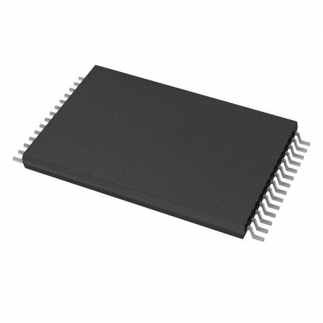
S29AS016J 3. Connection Diagrams 3.1 Standard TSOP A15 1 48 A16 A14 2 47 BYTE# A13 3 46 V SS A12 4 45 DQ15/A-1 A11 5 44 DQ7 A10 6 43 DQ14 A9 7 42 DQ6 A8 8 41 DQ13 A19 9 40 DQ5 NC 10 39 DQ12 WE# 11 38 DQ4 Standard TSOP RESET# 12 37 V CC NC 13 36 DQ11 WP# 14 35 DQ3 RY/BY# 15 34 DQ10 A18 16 33 DQ2 A17 17 32 DQ9 A7 18 31 DQ1 A6 19 30 DQ8 A5 20 29 DQ0 A4 21 28 OE# A3 22 27 V SS A2 23 26 CE# A1 24 25 A0 Document Number: 002-01122 Rev. *M Page 5 of 57
S29AS016J 3.2 FBGA Connection Diagram, 8.15 mm x 6.15 mm (VBK048) Fine-pitch Ball Grid Array - VBK048 Top View, Balls Facing Down A6 B6 C6 D6 E6 F6 G6 H6 A13 A12 A14 A15 A16 BYTE# DQ15/A-1 V SS A5 B5 C5 D5 E5 F5 G5 H5 A9 A8 A10 A11 DQ7 DQ14 DQ13 DQ6 A4 B4 C4 D4 E4 F4 G4 H4 WE# RESET# NC A19 DQ5 DQ12 V DQ4 CC A3 B3 C3 D3 E3 F3 G3 H3 RY/BY# WP# A18 NC DQ2 DQ10 DQ11 DQ3 A2 B2 C2 D2 E2 F2 G2 H2 A7 A17 A6 A5 DQ0 DQ8 DQ9 DQ1 A1 B1 C1 D1 E1 F1 G1 H1 A3 A4 A2 A1 A0 CE# OE# V SS Document Number: 002-01122 Rev. *M Page 6 of 57
S29AS016J 3.3 FBGA Connection Diagram, 6.0 mm x 4.0 mm (VDF048) Fine-pitch Ball Grid Array - VDF048 Top View, Balls Facing Down A B C D E F G H J K L 6 A2 A4 A6 A17 NC NC WE# RESET# A9 A11 5 A1 A3 A7 WP# RY/BY# A10 A13 A14 4 A0 A5 A18 A8 A12 A15 3 CE# DQ8 DQ10 DQ4 DQ11 A16 2 VSS OE# DQ9 A19 NC DQ5 DQ6 DQ7 1 DQ0 DQ1 DQ2 DQ3 VCC DQ12 DQ13 DQ14 DQ15 VSS 3.4 Special Handling Instructions Special handling is required for Flash Memory products in BGA packages. Flash memory devices in BGA packages may be damaged if exposed to ultrasonic cleaning methods. The package and/or data integrity may be compromised if the package body is exposed to temperatures above 150°C for prolonged periods of time. Document Number: 002-01122 Rev. *M Page 7 of 57
S29AS016J 4. Pin Configuration A0–A19 20 addresses DQ0–DQ14 15 data inputs/outputs DQ15/A-1 DQ15 (data input/output, word mode), A-1 (LSB address input, byte mode) BYTE# Selects 8-bit or 16-bit mode CE# Chip enable OE# Output enable WE# Write enable WP# Write protect: The WP# contains an internal pull-up; when unconnected, WP is at V . IH RESET# Hardware reset pin RY/BY# Ready/Busy output 1.8 volt-only single power supply (see Section1. Product Selector Guide onpage4 for speed options and V CC voltage supply tolerances) V Device ground SS NC Pin not connected internally 5. Logic Symbol 20 A0–A19 16 or 8 DQ0–DQ15 (A-1) CE# OE# WE# RESET# BYTE# RY/BY# WP# Document Number: 002-01122 Rev. *M Page 8 of 57
S29AS016J 6. Ordering Information 6.1 S29AS016J Standard Products Cypress standard products are available in several packages and operating ranges. The order number (Valid Combination) is formed by a combination of the elements below. S29AS016J 70 T F I 01 0 Packing Type 0 = Tray 2 = 7” Tape and Reel 3 = 13” Tape and Reel Model Number 03 = V = 1.65–1.95 V, top boot sector device CC 04 = V = 1.65–1.95 V, bottom boot sector device CC F3 = V = 1.65–1.95 V, x16 only, 6.0x4.0 mm FBGA, top boot sector device CC F4 = V = 1.65–1.95 V, x16 only, 6.0x4.0 mm FBGA, bottom boot sector device CC Temperature Range I = Industrial (-40°C to +85°C) V = Industrial Plus (-40°C to +105°C) A = Automotive, AEC-Q100 Grade 3 (-40 °C to +85 °C) B = Automotive, AEC-Q100 Grade 2 (-40 °C to +105 °C) Package Material Set F = Pb-Free H = Low-Halogen, Pb-Free Package Type T = Thin Small Outline Package (TSOP) Standard Pinout B = Fine-pitch Ball-Grid Array Package Speed Option 70 = 70 ns Access Speed 90 = 90 ns Access Speed Device Number/Description S29AS016J 16 Megabit Flash Memory manufactured using 110 nm process technology 1.8 Volt-only Read, Program, and Erase Document Number: 002-01122 Rev. *M Page 9 of 57
S29AS016J 6.1.1 Valid Combinations Valid Combinations list configurations planned to be supported in volume for this device. Contact your local sales office to confirm availability of specific valid combinations and to check on newly released combinations. S29AS016J Valid Combinations Package Type, Package Device Speed Material, and Model Packing Type Description Number Option Number Temperature Range TFI 0, 3[2] TS048[3] TSOP 03, 04 BFI, BHI VBK048 70 S29AS016J BFVB,H BIHV F033,, 0F44 0, 2, 3[2] VVBDKF004488 FiBneG-AP[i4tc]h 90 BFV, BHV 03, 04 VBK048 6.1.2 Valid Combinations - Automotive Grade / AEC-Q100 Valid Combinations list configurations that are Automotive Grade / AEC-Q100 qualified and are planned to be available in volume. This table will be updated as new combinations are released. Contact your local sales representative to confirm availability of specific combinations and to check on newly released combinations. Production Part Approval Process (PPAP) support is only provided for AEC-Q100 grade products. Products to be used in end-use applications that require ISO/TS-16949 compliance must be AEC-Q100 grade products in combination with PPAP. Non-AEC-Q100 grade products are not manufactured or documented in full compliance with ISO/TS-16949 requirements. AEC-Q100 grade products are also offered without PPAP support for end-use applications that do not require ISO/TS-16949 compliance. S29AS016J Valid Combinations Package Type, Package Device Speed Material, and Model Packing Type Description Number Option Number Temperature Range TFA 0, 3[2] TS048[3] TSOP 03, 04 BFA, BHA VBK048 70 S29AS016J BFBBH, BAHB F033,, F044 0, 2, 3[2] VVBDKF004488 FiBneG-AP[i4tc]h 90 BFB, BHB 03, 04 VBK048 Notes 2. Type 0 is standard. Specify other options as required. 3. TSOP package markings omit packing type designator from ordering part number. 4. BGA package marking omits leading “S29” and packing type designator from ordering part number. Document Number: 002-01122 Rev. *M Page 10 of 57
S29AS016J 7. Device Bus Operations This section describes the requirements and use of the device bus operations, which are initiated through the internal command register. The command register itself does not occupy any addressable memory location. The register is composed of latches that store the commands, along with the address and data information needed to execute the command. The contents of the register serve as inputs to the internal state machine. The state machine outputs dictate the function of the device. Table1 lists the device bus operations, the inputs and control levels they require, and the resulting output. The following subsections describe each of these operations in further detail. Table 1. S29AS016J Device Bus Operations DQ8–DQ15 Operation CE# OE# WE# RESET# WP# Addresses[5] DQ0–DQ7 BYTE# BYTE# = V = V IL IH Read L L H H X A D D IN OUT OUT DQ8–DQ14 = High-Z, DQ15 = Write L H L H Note A D D A-1 (Program/Erase) [7] IN IN IN V V Standby CC X X CC H X High-Z High-Z High-Z 0.2 V 0.2 V Output Disable L H H H X X High-Z High-Z High-Z Reset X X X L X X High-Z High-Z High-Z Sector Address, Sector Group Protect[6] L H L VID X A6 = L, A3 = A2 = DIN X X L, A1 = H, A0 = L Sector Address, Sector GroupUnprotect[6] L H L VID H A6 = H, A3 = A2 = DIN X X L, A1 = H, A0 = L Temporary Sector X X X V H A D D High-Z Group Unprotect ID IN IN IN Notes 5. Addresses are A19:A0 in word mode (BYTE# = VIH), A19:A-1 in byte mode (BYTE# = VIL). 6. The sector group protect and sector group unprotect functions may also be implemented via programming equipment. See Section7.11 Sector Group Protection/Un- protection onpage17. 7. If WP# = VIL, the two outermost boot sectors remain protected. If WP# = VIH, the two outermost boot sector group protection depends on whether they were last protected or unprotected. Legend L = Logic Low = VIL, H = Logic High = VIH, VID = 9.0 - 11.0 V, X = Don’t Care, AIN = Address In, DIN = Data In, DOUT = Data Out Document Number: 002-01122 Rev. *M Page 11 of 57
S29AS016J 7.1 Word/Byte Configuration The BYTE# pin controls whether the device data I/O pins DQ15–DQ0 operate in the byte or word configuration. If the BYTE# pin is set at logic 1, the device is in word configuration, DQ15–DQ0 are active and controlled by CE# and OE#. If the BYTE# pin is set at logic 0, the device is in byte configuration, and only data I/O pins DQ0–DQ7 are active and controlled by CE# and OE#. The data I/O pins DQ8–DQ14 are tri-stated, and the DQ15 pin is used as an input for the LSB (A-1) address function. 7.2 Requirements for Reading Array Data To read array data from the outputs, the system must drive the CE# and OE# pins to V . CE# is the power control and selects the IL device. OE# is the output control and gates array data to the output pins. WE# should remain at V . The BYTE# pin determines IH whether the device outputs array data in words or bytes. The internal state machine is set for reading array data upon device power-up, or after a hardware reset. This ensures that no spurious alteration of the memory content occurs during the power transition. No command is necessary in this mode to obtain array data. Standard microprocessor read cycles that assert valid addresses on the device address inputs produce valid data on the device data outputs. The device remains enabled for read access until the command register contents are altered. See Section10.1 Reading Array Data onpage27 for more information. Refer to the AC Section18.1 Read Operations onpage42 for timing specifications and Figure12 onpage42 for the timing diagram. I in Section15. DC Characteristics onpage40 CC1 represents the active current specification for reading array data. 7.3 Writing Commands/Command Sequences To write a command or command sequence (which includes programming data to the device and erasing sectors of memory), the system must drive WE# and CE# to V , and OE# to V . IL IH For program operations, the BYTE# pin determines whether the device accepts program data in bytes or words. See Section7.1 Word/Byte Configuration onpage12 for more information. The device features an Unlock Bypass mode to facilitate faster programming. Once the device enters the Unlock Bypass mode, only two write cycles are required to program a word or byte, instead of four. Section10.5 Word/Byte Program Command Sequence onpage28 has details on programming data to the device using both standard and Unlock Bypass command sequences. An erase operation can erase one sector, multiple sectors, or the entire device. Table3 onpage15 and Table4 onpage16 indicate the address space that each sector occupies. A “sector address” consists of the address bits required to uniquely select a sector. The Section10. Command Definitions onpage27 has details on erasing a sector or the entire chip, or suspending/resuming the erase operation. After the system writes the autoselect command sequence, the device enters the autoselect mode. The system can then read autoselect codes from the internal register (which is separate from the memory array) on DQ7–DQ0. Standard read cycle timings apply in this mode. Refer to Section7.9 Autoselect Mode onpage14 and Section10.3 Autoselect Command Sequence onpage27 for more information. I in Section15. DC Characteristics onpage40 represents the active current specification for the write mode. Section18. AC CC2 Characteristics onpage42 contains timing specification tables and timing diagrams for write operations. 7.4 Program and Erase Operation Status During an erase or program operation, the system may check the status of the operation by reading the status bits on DQ7–DQ0. Standard read cycle timings and I read specifications apply. Refer to Section12. Write Operation Status onpage34 for more CC information, and to Section18. AC Characteristics onpage42 for timing diagrams. Document Number: 002-01122 Rev. *M Page 12 of 57
S29AS016J 7.5 Standby Mode When the system is not reading or writing to the device, it can place the device in the standby mode. In this mode, current consumption is greatly reduced, and the outputs are placed in the high impedance state, independent of the OE# input. The device enters the CMOS standby mode when the CE# and RESET# pins are both held at V 0.2 V. (Note that this is a more CC restricted voltage range than V .) If CE# and RESET# are held at V , but not within V 0.2 V, the device will be in the standby IH IH CC mode, but the standby current will be greater. The device requires standard access time (t ) for read access when the device is in CE either of these standby modes, before it is ready to read data. If the device is deselected during erasure or programming, the device draws active current until the operation is completed. I and I represents the standby current specification shown in the table in Section15. DC Characteristics onpage40. CC3 CC4 7.6 Automatic Sleep Mode The automatic sleep mode minimizes Flash device energy consumption. The device automatically enables this mode when addresses remain stable for t + 30 ns. The automatic sleep mode is independent of the CE#, WE#, and OE# control signals. ACC Standard address access timings provide new data when addresses are changed. While in sleep mode, output data is latched and always available to the system. I in the Section15. DC Characteristics onpage40 represents the automatic sleep mode current CC5 specification. 7.7 RESET#: Hardware Reset Pin The RESET# pin provides a hardware method of resetting the device to reading array data. When the system drives the RESET# pin to V for at least a period of t , the device immediately terminates any operation in progress, tristates all data output pins, and IL RP ignores all read/write attempts for the duration of the RESET# pulse. The device also resets the internal state machine to reading array data. The operation that was interrupted should be reinitiated once the device is ready to accept another command sequence, to ensure data integrity. Current is reduced for the duration of the RESET# pulse. When RESET# is held at V ±0.2 V, the device draws CMOS standby SS current (I ). If RESET# is held at V but not within V ±0.2 V, the standby current will be greater. CC4 IL SS The RESET# pin may be tied to the system reset circuitry. A system reset would thus also reset the Flash memory, enabling the system to read the boot-up firmware from the Flash memory. Note that the CE# pin should only go to V after RESET# has gone to IL V . Keeping CE# at V from power up through the first read could cause the first read to retrieve erroneous data. IH IL If RESET# is asserted during a program or erase operation, the RY/BY# pin remains a 0 (busy) until the internal reset operation is complete, which requires a time of t (during Embedded Algorithms). The system can thus monitor RY/BY# to determine READY whether the reset operation is complete. If RESET# is asserted when a program or erase operation is not executing (RY/BY# pin is 1), the reset operation is completed within a time of t (not during Embedded Algorithms). The system can read data t after READY RH the RESET# pin returns to V . IH Refer to the tables in Section18. AC Characteristics onpage42 for RESET# parameters and to Figure13 onpage43 for the timing diagram. If V (9.0 V – 11.0 V) is applied to the RESET# pin, the device will enter the Temporary Sector Group Unprotect mode. ID See Section7.12 Temporary Sector Group Unprotect onpage20 for more details on this feature. 7.8 Output Disable Mode When the OE# input is at V , output from the device is disabled. The output pins are placed in the high impedance state. IH Document Number: 002-01122 Rev. *M Page 13 of 57
S29AS016J 7.9 Autoselect Mode The autoselect mode provides manufacturer and device identification, sector group protection verification, and Secured Silicon Sector status through identifier codes output on DQ7–DQ0. This mode is primarily intended for programming equipment to automatically match a device to be programmed with its corresponding programming algorithm. However, the autoselect codes can also be accessed in-system through the command register. When using programming equipment, the autoselect mode requires V (9.0 V to 11.0 V) on address pin A9. Address pins A6, A3, ID A2, A1, and A0 must be as shown in Table2. In addition, when verifying sector group protection, the sector address must appear on the appropriate highest order address bits (see Table 3 on page 15 and Table 4 on page 16). Table2 shows the remaining address bits that are don’t care. When all necessary bits have been set as required, the programming equipment may then read the corresponding identifier code on DQ7-DQ0. To access the autoselect codes in-system, the host system can issue the autoselect command via the command register, as shown in Table 11 on page 32. This method does not require V . See Section10. Command Definitions onpage27 for details on using the ID autoselect mode. Table 2. S29AS016J Autoselect Codes (HighVoltageMethod) A19 A11 A8 A5 A3 DQ8 to DQ15 DQ7 to Description CE# OE# WE# to to A9 to A6 to to A1 A0 BYTE BYTE DQ0 A12 A10 A7 A4 A2 = V = V IH IL Manufacturer ID: L L H X X V X L X L L L 00h X 01h Cypress ID Cycle 1 L L H X X V X L X L L H 22h X 7Eh ID Device Cycle 2 L L H X X V X L X H H L 22h X 03h ID ID 04h (Top Boot), Cycle 3 L L H X X V X L X H H H 22h X ID 03h (Bottom Boot) Sector Group 01h (protected), Protection L L H SA X V X L X L H L X X ID 00h (unprotected) Verification Secured Silicon Sector Indicator Bit 89h (factory locked), (DQ7), WP# L L H X X V X L X L H H X X ID 09h (not factory locked) protects highest address sector Secured Silicon Sector Indicator Bit 91h (factory locked), (DQ7), WP# L L H X X V X L X L H H X X ID 11h (not factory locked) protects lowest address sector Note 8. The autoselect codes may also be accessed in-system via command sequences. See Table11 onpage32. Legend L = Logic Low = VIL, H = Logic High = VIH, SA = Sector Address, X = Don’t care Document Number: 002-01122 Rev. *M Page 14 of 57
S29AS016J 7.10 Sector Address Tables Table 3. Sector Address Table (Top Boot Device) Sector Size Address Range (in hexadecimal) Sector A19 A18 A17 A16 A15 A14 A13 A12 (Kbytes/Kwords) Byte Mode (x8) Word Mode (x16) SA0 0 0 0 0 0 X X X 64/32 000000–00FFFF 00000–07FFF SA1 0 0 0 0 1 X X X 64/32 010000–01FFFF 08000–0FFFF SA2 0 0 0 1 0 X X X 64/32 020000–02FFFF 10000–17FFF SA3 0 0 0 1 1 X X X 64/32 030000–03FFFF 18000–1FFFF SA4 0 0 1 0 0 X X X 64/32 040000–04FFFF 20000–27FFF SA5 0 0 1 0 1 X X X 64/32 050000–05FFFF 28000–2FFFF SA6 0 0 1 1 0 X X X 64/32 060000–06FFFF 30000–37FFF SA7 0 0 1 1 1 X X X 64/32 070000–07FFFF 38000–3FFFF SA8 0 1 0 0 0 X X X 64/32 080000–08FFFF 40000–47FFF SA9 0 1 0 0 1 X X X 64/32 090000–09FFFF 48000–4FFFF SA10 0 1 0 1 0 X X X 64/32 0A0000–0AFFFF 50000–57FFF SA11 0 1 0 1 1 X X X 64/32 0B0000–0BFFFF 58000–5FFFF SA12 0 1 1 0 0 X X X 64/32 0C0000–0CFFFF 60000–67FFF SA13 0 1 1 0 1 X X X 64/32 0D0000–0DFFFF 68000–6FFFF SA14 0 1 1 1 0 X X X 64/32 0E0000–0EFFFF 70000–77FFF SA15 0 1 1 1 1 X X X 64/32 0F0000–0FFFFF 78000–7FFFF SA16 1 0 0 0 0 X X X 64/32 100000–10FFFF 80000–87FFF SA17 1 0 0 0 1 X X X 64/32 110000–11FFFF 88000–8FFFF SA18 1 0 0 1 0 X X X 64/32 120000–12FFFF 90000–97FFF SA19 1 0 0 1 1 X X X 64/32 130000–13FFFF 98000–9FFFF SA20 1 0 1 0 0 X X X 64/32 140000–14FFFF A0000–A7FFF SA21 1 0 1 0 1 X X X 64/32 150000–15FFFF A8000–AFFFF SA22 1 0 1 1 0 X X X 64/32 160000–16FFFF B0000–B7FFF SA23 1 0 1 1 1 X X X 64/32 170000–17FFFF B8000–BFFFF SA24 1 1 0 0 0 X X X 64/32 180000–18FFFF C0000–C7FFF SA25 1 1 0 0 1 X X X 64/32 190000–19FFFF C8000–CFFFF SA26 1 1 0 1 0 X X X 64/32 1A0000–1AFFFF D0000–D7FFF SA27 1 1 0 1 1 X X X 64/32 1B0000–1BFFFF D8000–DFFFF SA28 1 1 1 0 0 X X X 64/32 1C0000–1CFFFF E0000–E7FFF SA29 1 1 1 0 1 X X X 64/32 1D0000–1DFFFF E8000–EFFFF SA30 1 1 1 1 0 X X X 64/32 1E0000–1EFFFF F0000–F7FFF SA31 1 1 1 1 1 0 0 0 8/4 1F0000–1F1FFF F8000–F8FFF SA32 1 1 1 1 1 0 0 1 8/4 1F2000–1F3FFF F9000–F9FFF SA33 1 1 1 1 1 0 1 0 8/4 1F4000–1F5FFF FA000–FAFFF SA34 1 1 1 1 1 0 1 1 8/4 1F6000–1F7FFF FB000–FBFFF SA35 1 1 1 1 1 1 0 0 8/4 1F8000–1F9FFF FC000–FCFFF SA36 1 1 1 1 1 1 0 1 8/4 1FA000–1FBFFF FD000–FDFFF SA37 1 1 1 1 1 1 1 0 8/4 1FC000–1FDFFF FE000–FEFFF SA38 1 1 1 1 1 1 1 1 8/4 1FE000–1FFFFF FF000–FFFFF Note 9. Address range is A19:A-1 in byte mode and A19:A0 in word mode. See Section7.1 Word/Byte Configuration onpage12. Document Number: 002-01122 Rev. *M Page 15 of 57
S29AS016J Table 4. Sector Address Table (Bottom Boot Device) Sector Size Address Range (in hexadecimal) Sector A19 A18 A17 A16 A15 A14 A13 A12 (Kbytes/Kwords) Byte Mode (x8) Word Mode (x16) SA0 0 0 0 0 0 0 0 0 8/4 000000–001FFF 00000–00FFF SA1 0 0 0 0 0 0 0 1 8/4 002000–003FFF 01000–01FFF SA2 0 0 0 0 0 0 1 0 8/4 004000–005FFF 02000–02FFF SA3 0 0 0 0 0 0 1 1 8/4 006000–007FFF 03000–03FFF SA4 0 0 0 0 0 1 0 0 8/4 008000–009FFF 04000–04FFF SA5 0 0 0 0 0 1 0 1 8/4 00A000–00BFFF 05000–05FFF SA6 0 0 0 0 0 1 1 0 8/4 00C000–00DFFF 06000–06FFF SA7 0 0 0 0 0 1 1 1 8/4 00E000–00FFFF 07000–07FFF SA8 0 0 0 0 1 X X X 64/32 010000–01FFFF 08000–0FFFF SA9 0 0 0 1 0 X X X 64/32 020000–02FFFF 10000–17FFF SA10 0 0 0 1 1 X X X 64/32 030000–03FFFF 18000–1FFFF SA11 0 0 1 0 0 X X X 64/32 040000–04FFFF 20000–27FFF SA12 0 0 1 0 1 X X X 64/32 050000–05FFFF 28000–2FFFF SA13 0 0 1 1 0 X X X 64/32 060000–06FFFF 30000–37FFF SA14 0 0 1 1 1 X X X 64/32 070000–07FFFF 38000–3FFFF SA15 0 1 0 0 0 X X X 64/32 080000–08FFFF 40000–47FFF SA16 0 1 0 0 1 X X X 64/32 090000–09FFFF 48000–4FFFF SA17 0 1 0 1 0 X X X 64/32 0A0000–0AFFFF 50000–57FFF SA18 0 1 0 1 1 X X X 64/32 0B0000–0BFFFF 58000–5FFFF SA19 0 1 1 0 0 X X X 64/32 0C0000–0CFFFF 60000–67FFF SA20 0 1 1 0 1 X X X 64/32 0D0000–0DFFFF 68000–6FFFF SA21 0 1 1 1 0 X X X 64/32 0E0000–0EFFFF 70000–77FFF SA22 0 1 1 1 1 X X X 64/32 0F0000–0FFFFF 78000–7FFFF SA23 1 0 0 0 0 X X X 64/32 100000–10FFFF 80000–87FFF SA24 1 0 0 0 1 X X X 64/32 110000–11FFFF 88000–8FFFF SA25 1 0 0 1 0 X X X 64/32 120000–12FFFF 90000–97FFF SA26 1 0 0 1 1 X X X 64/32 130000–13FFFF 98000–9FFFF SA27 1 0 1 0 0 X X X 64/32 140000–14FFFF A0000–A7FFF SA28 1 0 1 0 1 X X X 64/32 150000–15FFFF A8000–AFFFF SA29 1 0 1 1 0 X X X 64/32 160000–16FFFF B0000–B7FFF SA30 1 0 1 1 1 X X X 64/32 170000–17FFFF B8000–BFFFF SA31 1 1 0 0 0 X X X 64/32 180000–18FFFF C0000–C7FFF SA32 1 1 0 0 1 X X X 64/32 190000–19FFFF C8000–CFFFF SA33 1 1 0 1 0 X X X 64/32 1A0000–1AFFFF D0000–D7FFF SA34 1 1 0 1 1 X X X 64/32 1B0000–1BFFFF D8000–DFFFF SA35 1 1 1 0 0 X X X 64/32 1C0000–1CFFFF E0000–E7FFF SA36 1 1 1 0 1 X X X 64/32 1D0000–1DFFFF E8000–EFFFF SA37 1 1 1 1 0 X X X 64/32 1E0000–1EFFFF F0000–F7FFF SA38 1 1 1 1 1 X X X 64/32 1F0000–1FFFFF F8000–FFFFF Note 10.Address range is A19:A-1 in byte mode and A19:A0 in word mode. See Section7.1 Word/Byte Configuration onpage12. Document Number: 002-01122 Rev. *M Page 16 of 57
S29AS016J 7.11 Sector Group Protection/Unprotection The hardware sector group protection feature disables both program and erase operations in any sector group (see Table3 onpage15 to Table6 onpage18). The hardware sector group unprotection feature re-enables both program and erase operations in previously protected sector groups. Sector group protection/unprotection can be implemented via two methods. Sector group protection/unprotection requires VID on the RESET# pin only, and can be implemented either in-system or via programming equipment. Figure1 onpage19 shows the algorithms and Figure12 onpage42 shows the timing diagram. This method uses standard microprocessor bus cycle timing. For sector group unprotect, all unprotected sector groups must first be protected prior to the first sector group unprotect write cycle. The device is shipped with all sector groups unprotected. Cypress offers the option of programming and protecting sector groups at its factory prior to shipping the device through Cypress Programming Service. Contact a Cypress representative for details. It is possible to determine whether a sector group is protected or unprotected. See Section7.9 Autoselect Mode onpage14 for details. Table 5. AS016J Top Boot Device Sector/Sector Group Protection Sector / Sector Block A19 A18 A17 A16 A15 A14 A13 A12 Sector / Sector Block Size SA0-SA3 0 0 0 X X X X X 256 (4x64) Kbytes SA4-SA7 0 0 1 X X X X X 256 (4x64) Kbytes SA8-SA11 0 1 0 X X X X X 256 (4x64) Kbytes SA12-SA15 0 1 1 X X X X X 256 (4x64) Kbytes SA16-SA19 1 0 0 X X X X X 256 (4x64) Kbytes SA20-SA23 1 0 1 X X X X X 256 (4x64) Kbytes SA24-SA27 1 1 0 X X X X X 256 (4x64) Kbytes SA28-SA29 1 1 1 0 X X X X 128 (2x64) Kbytes SA30 1 1 1 1 0 X X X 64 Kbytes SA31 1 1 1 1 1 0 0 0 8 Kbytes SA32 1 1 1 1 1 0 0 1 8 Kbytes SA33 1 1 1 1 1 0 1 0 8 Kbytes SA34 1 1 1 1 1 0 1 1 8 Kbytes SA35 1 1 1 1 1 1 0 0 8 Kbytes SA36 1 1 1 1 1 1 0 1 8 Kbytes SA37 1 1 1 1 1 1 1 0 8 Kbytes SA38 1 1 1 1 1 1 1 1 8 Kbytes Document Number: 002-01122 Rev. *M Page 17 of 57
S29AS016J Table 6. AS016J Bottom Boot Device Sector/Sector Group Protection Sector / Sector Block A19 A18 A17 A16 A15 A14 A13 A12 Sector / Sector Block Size SA0 0 0 0 0 0 0 0 0 8 Kbytes SA1 0 0 0 0 0 0 0 1 8 Kbytes SA2 0 0 0 0 0 0 1 0 8 Kbytes SA3 0 0 0 0 0 0 1 1 8 Kbytes SA4 0 0 0 0 0 1 0 0 8 Kbytes SA5 0 0 0 0 0 1 0 1 8 Kbytes SA6 0 0 0 0 0 1 1 0 8 Kbytes SA7 0 0 0 0 0 1 1 1 8 Kbytes SA8 0 0 0 0 1 X X X 64 Kbytes SA9-SA10 0 0 0 1 X X X X 128 (2x64) Kbytes SA11-SA14 0 0 1 X X X X X 256 (4x64) Kbytes SA15-SA18 0 1 0 X X X X X 256 (4x64) Kbytes SA19-SA22 0 1 1 X X X X X 256 (4x64) Kbytes SA23-SA26 1 0 0 X X X X X 256 (4x64) Kbytes SA27-SA30 1 0 1 X X X X X 256 (4x64) Kbytes SA31-SA34 1 1 0 X X X X X 256 (4x64) Kbytes SA35-SA38 1 1 1 X X X X X 256 (4x64) Kbytes Document Number: 002-01122 Rev. *M Page 18 of 57
S29AS016J Figure 1.In-System Sector Group Protect/Unprotect Algorithms START START PLSCNT = 1 Protect all sectors: The indicated portion PLSCNT = 1 of the sector group RESET# = VID protect algorithm must be performed RESET# = VID Wait 1 µs for all unprotected sector groups prior Wait 1 µs to issuing the first Temporary Sector No First Write unsperoctteocr tg arodudpre ss Group Unprotect Mode Cycle = 60h? First Write No Temporary Sector Cycle = 60h? Group Unprotect Mode Yes Yes Set up sector address No All sectors protected? Sector Group Protect: Write 60h to sector address with Yes A6 = 0, Set up first sector A3 = A2 = 0, group address A1 = 1, A0 = 0 Sector Group Unprotect: Wait 100 µs Write 60h to sector address with Verify Sector Group A6 = 1, A1 = 1, Protect: Write 40h A0 = 0 to sector address Reset Increment with A6 = 0, PLSCNT = 1 Wait 10 ms PLSCNT A3 = A2 = 0, A1 = 1, A0 = 0 Verify Sector Group Unprotect: Write Read from 40h to sector sector address address with with A6 = 0, Increment A6 = 1, A1 = 1, A3 = A2 = 0, PLSCNT A0 = 0 A1 = 1, A0 = 0 No Read from sector address No with A6 = 1, PLSCNT Data = 01h? A3 = A2 = 0, = 25? A1 = 1, A0 = 0 No Yes Set up Yes next sector No PLSCNT Data = 00h? address Yes = 1000? Protect another Device failed sector? Yes Yes No Last sector No Remove VID Device failed group verified? from RESET# Yes Write reset command Remove VID Sector Group Sector Group from RESET# Protect Algorithm Unprotect Algorithm Sector Group Protect complete Write reset command Sector Group Unprotect complete Note 11.If WP# = VIL, the top or bottom two address sectors remains protected for boot sector devices). Document Number: 002-01122 Rev. *M Page 19 of 57
S29AS016J 7.12 Temporary Sector Group Unprotect This feature allows temporary unprotection of previously protected sectors to change data in-system. The Sector Group Unprotect mode is activated by setting the RESET# pin to V . During this mode, formerly protected sectors can be programmed or erased by ID selecting the sector addresses. Once V is removed from the RESET# pin, all the previously protected sectors are protectedagain. ID Figure2 shows the algorithm, and Figure21 onpage48 shows the timing diagrams, for this feature. If the WP# pin is at V , the IL sectors protected by the WP# input will remain protected during the Temporary Sector Group Unprotect mode. Figure 2. Temporary Sector Group Unprotect Operation START RESET# = V ID (Note 12) Perform Erase or Program Operations RESET# = V IH Temporary Sector Group Unprotect Completed (Note 13) 7.13 Write Protect (WP#) The Write Protect function provides a hardware method of protecting certain boot sectors without using VID. This function is one of two provided by the WP# pin. If the system asserts V on the WP# pin, the device disables program and erase functions in the two outermost 8-Kbyte boot IL sectors independently of whether those sectors were protected or unprotected using the method described in Section7.11 Sector Group Protection/Unprotection onpage17. The two outermost 8-Kbyte boot sectors are the two sectors containing the lowest addresses in a bottom-boot-configured device, or the two sectors containing the highest addresses in a top-boot-configured device. If the system asserts V on the WP# pin, the device reverts to whether the two outermost 8-KByte boot sectors were last set to be IH protected or unprotected. That is, sector group protection or unprotection for these two sectors depends on whether they were last protected or unprotected using the method described in Section7.11 Sector Group Protection/Unprotection onpage17. The WP# contains an internal pull-up; when unconnected, WP is at V . IH 7.14 Hardware Data Protection The command sequence requirement of unlock cycles for programming or erasing provides data protection against inadvertent writes (refer to Table11 onpage32 for command definitions). In addition, the following hardware data protection measures prevent accidental erasure or programming, which might otherwise be caused by spurious system level signals during V power-up and CC power-down transitions, or from system noise. Notes 12.All protected sector groups unprotected. 13.All previously protected sector groups are protected once again. Document Number: 002-01122 Rev. *M Page 20 of 57
S29AS016J 7.14.1 Low V Write Inhibit CC When V is less than V , the device does not accept any write cycles. This protects data during V power-up and power-down. CC LKO CC The command register and all internal program/erase circuits are disabled, and the device resets. Subsequent writes are ignored until V is greater than V . The system must provide the proper signals to the control pins to prevent unintentional writes when CC LKO V is greater than V . CC LKO 7.14.2 Write Pulse Glitch Protection Noise pulses of less than 5 ns (typical) on OE#, CE# or WE# do not initiate a write cycle. 7.14.3 Logical Inhibit Write cycles are inhibited by holding any one of OE# = V , CE# = V or WE# = V . To initiate a write cycle, CE# and WE# must be IL IH IH a logical zero (V ) while OE# is a logical one (V ). IL IH 7.14.4 Power-Up Write Inhibit If WE# = CE# = V and OE# = V during power up, the device does not accept commands on the rising edge of WE#. The internal IL IH state machine is automatically reset to reading array data on power-up. Document Number: 002-01122 Rev. *M Page 21 of 57
S29AS016J 8. Secured Silicon Sector Flash Memory Region The Secured Silicon Sector feature provides a 256-byte Flash memory region that enables permanent part identification through an Electronic Serial Number (ESN). The Secured Silicon Sector uses a Secured Silicon Sector Indicator Bit (DQ7) to indicate whether or not the Secured Silicon Sector is locked when shipped from the factory. This bit is permanently set at the factory and cannot be changed, which prevents cloning of a factory-locked part. This ensures the security of the ESN once the product is shipped to the field. Cypress offers the device with the Secured Silicon Sector either factory-locked or customer-lockable. The factory-locked version is always protected when shipped from the factory, and has the Secured Silicon Sector Indicator Bit permanently set to a 1. The customer-lockable version is shipped with the Secured Silicon Sector group unprotected, allowing customers to utilize the that sector in any manner they choose. The customer-lockable version has the Secured Silicon Sector Indicator Bit permanently set to a 0. Thus, the Secured Silicon Sector Indicator Bit prevents customer-lockable devices from being used to replace devices that are factory locked. The system accesses the Secured Silicon Sector through a command sequence (see Section10.4 Enter Secured Silicon Sector/Exit Secured Silicon Sector Command Sequence onpage28). After the system writes the Enter Secured Silicon Sector command sequence, it may read the Secured Silicon Sector by using the addresses normally occupied by the boot sectors. This mode of operation continues until the system issues the Exit Secured Silicon Sector command sequence, or until power is removed from the device. On power-up, or following a hardware reset, the device reverts to sending commands to the boot sectors. 8.1 Factory Locked: Secired Silicon Sector Programmed and Protected at the Factory In a factory locked device, the Secured Silicon Sector is protected when the device is shipped from the factory. The Secured Silicon Sector cannot be modified in any way. The device is available pre-programmed with one of the following: A random, secure ESN only. Customer code through the ExpressFlash service. Both a random, secure ESN and customer code through the ExpressFlash service. In devices that have an ESN, a Bottom Boot device has the 16-byte (8-word) ESN in sector 0 at addresses 00000h–0000Fh in byte mode (or 00000h–00007h in word mode). In the Top Boot device, the ESN is in sector 38 at addresses 1FFFF0–1FFFFF in byte mode (or FFFF8–FFFFF in word mode). Customers may opt to have their code programmed by Cypress through the Cypress ExpressFlash service. Cypress programs the customer’s code, with or without the random ESN. The devices are then shipped from the Cypress factory with the Secured Silicon Sector permanently locked. Contact a Cypress representative for details on using the Cypress ExpressFlash service. 8.2 Customer Lockable: Secured Silicon Sector NOT Programmed or Protected at the Factory The customer lockable version allows the Secured Silicon Sector to be programmed once, and then permanently locked after it ships from Cypress. Note that the unlock bypass function is not available when programming the Secured Silicon Sector. The Secured Silicon Sector area can be protected using the following procedures: Write the three-cycle Enter Secured Silicon Region command sequence, and then follow the in-system sector group protect algorithm as shown in Figure 1 on page 19, substituting the sector group address with the Secured Silicon Sector group address (A0=0, A1=1, A2=0, A3=1, A4=1, A5=0, A6=0, A7=0). This allows in-system protection of the Secured Silicon Sector without raising any device pin to a high voltage. Note that this method is only applicable to the Secured Silicon Sector. To verify the protect/unprotect status of the Secured Silicon Sector, follow the algorithm shown in Figure3 onpage23. Once the Secured Silicon Sector is locked and verified, the system must write the Exit Secured Silicon Sector Region command sequence to return to reading and writing the remainder of the array. The Secured Silicon Sector protection must be used with caution since, once protected, there is no procedure available for unprotecting the Secured Silicon Sector area, and none of the bits in the Secured Silicon Sector memory space can be modified in any way. Document Number: 002-01122 Rev. *M Page 22 of 57
S29AS016J Figure 3. Secured Silicon Sector Protect Verify START If data = 00h, RESET# = V Secured Silicon ID Sector is unprotected. If data = 01h, Wait 1 ms Secured Silicon Sector is Write 60h to protected. any address Remove V ID Write 40h to from RESET# Secured Silicon Sector address with A0=0, A1=1, Write reset A2=0, A3=1, A4=1, command A5=0, A6=0, A7=0 Secured Silicon Read from Sector Protect Secured Silicon Verify complete Sector address with A0=0, A1=1, A2=0, A3=1, A4=1, A5=0, A6=0, A7=0 Document Number: 002-01122 Rev. *M Page 23 of 57
S29AS016J 9. Common Flash Memory Interface (CFI) The Common Flash Interface (CFI) specification outlines device and host system software interrogation handshake, which allows specific vendor-specified software algorithms to be used for entire families of devices. Software support can then be device-independent, JEDEC ID-independent, and forward- and backward-compatible for the specified flash device families. Flash vendors can standardize their existing interfaces for long-term compatibility. This device enters the CFI Query mode when the system writes the CFI Query command, 98h, to address 55h in word mode (or address AAh in byte mode), any time the device is ready to read array data. The system can read CFI information at the addresses given in Table7 to Table10 onpage25. In word mode, the upper address bits (A7–MSB) must be all zeros. To terminate reading CFI data, the system must write the reset command. The system can also write the CFI query command when the device is in the autoselect mode. The device enters the CFI query mode, and the system can read CFI data at the addresses given in Table7 to Table10 onpage25. The system must write the reset command to return the device to the autoselect mode. Table 7. CFI Query Identification String Addresses Addresses (Word Mode) (Byte Mode) Data Description 10h 20h 0051h 11h 22h 0052h Query Unique ASCII string “QRY” 12h 24h 0059h 13h 26h 0002h Primary OEM Command Set 14h 28h 0000h 15h 2Ah 0040h Address for Primary Extended Table 16h 2Ch 0000h 17h 2Eh 0000h Alternate OEM Command Set (00h = none exists) 18h 30h 0000h 19h 32h 0000h Address for Alternate OEM Extended Table (00h = none exists) 1Ah 34h 0000h Table 8. System Interface String Addresses Addresses (Word Mode) (Byte Mode) Data Description V Min. (write/erase) 1Bh 36h 0017h CC D7–D4: volt, D3–D0: 100 millivolt V Max. (write/erase) 1Ch 38h 0019h CC D7–D4: volt, D3–D0: 100 millivolt 1Dh 3Ah 0000h V Min. voltage (00h = no V pin present) PP PP 1Eh 3Ch 0000h V Max. voltage (00h = no V pin present) PP PP 1Fh 3Eh 0003h Typical timeout per single byte/word write 2N µs 20h 40h 0000h Typical timeout for Min. size buffer write 2N µs (00h = not supported) 21h 42h 0009h Typical timeout per individual block erase 2N ms 22h 44h 0000h Typical timeout for full chip erase 2N ms (00h = not supported) 23h 46h 0005h Max. timeout for byte/word write 2N times typical 24h 48h 0000h Max. timeout for buffer write 2N times typical 25h 4Ah 0004h Max. timeout per individual block erase 2N times typical 26h 4Ch 0000h Max. timeout for full chip erase 2N times typical (00h = not supported) Document Number: 002-01122 Rev. *M Page 24 of 57
S29AS016J Table 9. Device Geometry Definition Addresses Addresses (Word Mode) (Byte Mode) Data Description 27h 4Eh 0015h Device Size = 2N byte 28h 50h 0002h Flash Device Interface description (refer to CFI publication 100) 29h 52h 0000h 2Ah 54h 0000h Max. number of byte in multi-byte write = 2N 2Bh 56h 0000h (00h = not supported) 2Ch 58h 0002h Number of Erase Block Regions within device 2Dh 5Ah 0007h 2Eh 5Ch 0000h Erase Block Region 1 Information 2Fh 5Eh 0020h (refer to the CFI specification or CFI publication 100) 30h 60h 0000h 31h 62h 001Eh 32h 64h 0000h Erase Block Region 2 Information 33h 66h 0000h 34h 68h 0001h 35h 6Ah 0000h 36h 6Ch 0000h Erase Block Region 3 Information 37h 6Eh 0000h 38h 70h 0000h 39h 72h 0000h 3Ah 74h 0000h Erase Block Region 4 Information 3Bh 76h 0000h 3Ch 78h 0000h Table 10. Primary Vendor-Specific Extended Query Addresses Addresses (Word Mode) (Byte Mode) Data Description 40h 80h 0050h 41h 82h 0052h Query-unique ASCII string “PRI” 42h 84h 0049h 43h 86h 0031h Major version number, ASCII 44h 88h 0033h Minor version number, ASCII Address Sensitive Unlock 45h 8Ah 000Ch 0 = Required 1 = Not Required Erase Suspend 0 = Not Supported 46h 8Ch 0002h 1 = To Read Only 2 = To Read & Write Sector Group Protect 47h 8Eh 0001h 0 = Not Supported X= Number of sectors in smallest sector group Sector Group Temporary Unprotect 48h 90h 0001h 00 = Not Supported 01 = Supported Document Number: 002-01122 Rev. *M Page 25 of 57
S29AS016J Table 10. Primary Vendor-Specific Extended Query (Continued) Addresses Addresses (Word Mode) (Byte Mode) Data Description Sector Group Protect/Unprotect scheme 01 = 29F040 mode 49h 92h 0004h 02 = 29F016 mode, 03 = 29F400 mode 04 = 29LV800A mode Simultaneous Operation 4Ah 94h 0000h 00 = Not Supported 01 = Supported Burst Mode Type 4Bh 96h 0000h 00 = Not Supported 01 = Supported Page Mode Type 00 = Not Supported 4Ch 98h 0000h 01 = 4 Word Page 02 = 8 Word Page ACC (Acceleration) Supply Minimum 00 = Not Supported 4Dh 9Ah 0000h D7-D4: Volt D3-D0: 100 mV ACC (Acceleration) Supply Maximum 00 = Not Supported 4Eh 9Ch 0000h D7-D4: Volt D3-D0: 100 mV WP# Protection 4Fh 9Eh 00XXh 02 = Bottom Boot Device with WP Protect 03 = Top Boot Device with WP Protect Program Suspend 50h A0h 0000h 00 = Not Supported 01 = Supported Document Number: 002-01122 Rev. *M Page 26 of 57
S29AS016J 10. Command Definitions Writing specific address and data commands or sequences into the command register initiates device operations. Table11 onpage32 defines the valid register command sequences. Writing incorrect address and data values or writing them in the improper sequence resets the device to reading array data. All addresses are latched on the falling edge of WE# or CE#, whichever happens later. All data is latched on the rising edge of WE# or CE#, whichever happens first. Refer to the appropriate timing diagrams in Section18. AC Characteristics onpage42. 10.1 Reading Array Data The device is automatically set to reading array data after device power-up. No commands are required to retrieve data. The device is also ready to read array data after completing an Embedded Program or Embedded Erase algorithm. After the device accepts an Erase Suspend command, the device enters the Erase Suspend mode. The system can read array data using the standard read timings, except that if it reads at an address within erase-suspended sectors, the device outputs status data. After completing a programming operation in the Erase Suspend mode, the system may once again read array data with the same exception. See Section10.9 Erase Suspend/Erase Resume Commands onpage30 for more information on this mode. The system must issue the reset command to re-enable the device for reading array data if DQ5 goes high, or while in the autoselect mode. See Section10.2 Reset Command onpage27. See also Requirements for Reading Array Data onpage12 for more information. The Section18.1 Read Operations onpage42 provides the read parameters, and Figure12 onpage42 shows the timing diagram. 10.2 Reset Command Writing the reset command to the device resets the device to reading array data. Address bits are don’t care for this command. The reset command may be written between the sequence cycles in an erase command sequence before erasing begins. This resets the device to reading array data. Once erasure begins, however, the device ignores reset commands until the operation is complete. The reset command may be written between the sequence cycles in a program command sequence before programming begins. This resets the device to reading array data (also applies to programming in Erase Suspend mode). Once programming begins, however, the device ignores reset commands until the operation is complete. The reset command may be written between the sequence cycles in an autoselect command sequence. Once in the autoselect mode, the reset command must be written to return to reading array data (also applies to autoselect during Erase Suspend). If DQ5 goes high during a program or erase operation, writing the reset command returns the device to reading array data (also applies during Erase Suspend). 10.3 Autoselect Command Sequence The autoselect command sequence allows the host system to access the manufacturer and devices codes, and determine whether or not a sector is protected. Table11 onpage32 shows the address and data requirements. This method is an alternative to that shown in Table2 onpage14, which is intended for PROM programmers and requires V on address bit A9. ID The autoselect command sequence is initiated by writing two unlock cycles, followed by the autoselect command. The device then enters the autoselect mode, and the system may read at any address any number of times, without initiating another command sequence. A read cycle at address XX00h retrieves the manufacturer code. A read cycle at address XX01h returns the device code. A read cycle containing a sector address (SA) and the address 02h in word mode (or 04h in byte mode) returns 01h if that sector is protected, or 00h if it is unprotected. Refer to Table3 onpage15 and Table4 onpage16 for valid sector addresses. The system must write the reset command to exit the autoselect mode and return to reading array data. Document Number: 002-01122 Rev. *M Page 27 of 57
S29AS016J 10.4 Enter Secured Silicon Sector/Exit Secured Silicon Sector Command Sequence The Secured Silicon Sector region provides a secured data area containing a random, sixteen-byte electronic serial number (ESN). The system can access the Secured Silicon Sector region by issuing the three-cycle Enter Secured Silicon Sector command sequence. The device continues to access the Secured Silicon Sector region until the system issues the four-cycle Exit Secured Silicon Sector command sequence. The Exit Secured Silicon Sector command sequence returns the device to normal operation. Table11 shows the addresses and data requirements for both command sequences. Note that the unlock bypass mode is not available when the device enters the Secured Silicon Sector. For further information, see Section8. Secured Silicon Sector Flash Memory Region onpage22. 10.5 Word/Byte Program Command Sequence The system may program the device by word or byte, depending on the state of the BYTE# pin. Programming is a four-bus-cycle operation. The program command sequence is initiated by writing two unlock write cycles, followed by the program set-up command. The program address and data are written next, which in turn initiate the Embedded Program algorithm. The system is not required to provide further controls or timings. The device automatically generates the program pulses and verifies the programmed cell margin. Table11 onpage32 shows the address and data requirements for the byte program command sequence. When the Embedded Program algorithm is complete, the device then returns to reading array data and addresses are no longer latched. The system can determine the status of the program operation by using DQ7, DQ6, or RY/BY#. See Section12. Write Operation Status onpage34 for information on these status bits. Any commands written to the device during the Embedded Program Algorithm are ignored. Note that a hardware reset immediately terminates the programming operation. The Byte Program command sequence should be reinitiated once the device has reset to reading array data, to ensure data integrity. Programming is allowed in any sequence and across sector boundaries. A bit cannot be programmed from a 0 back to a 1. Attempting to do so may halt the operation and set DQ5 to 1, or cause the Data# Polling algorithm to indicate the operation was successful. However, a succeeding read will show that the data is still 0. Only erase operations can convert a 0 to a 1. 10.6 Unlock Bypass Command Sequence The unlock bypass feature allows the system to program bytes or words to the device faster than using the standard program command sequence. The unlock bypass command sequence is initiated by first writing two unlock cycles. This is followed by a third write cycle containing the unlock bypass command, 20h. The device then enters the unlock bypass mode. A two-cycle unlock bypass program command sequence is all that is required to program in this mode. The first cycle in this sequence contains the unlock bypass program command, A0h; the second cycle contains the program address and data. Additional data is programmed in the same manner. This mode dispenses with the initial two unlock cycles required in the standard program command sequence, resulting in faster total programming time. Table11 onpage32 shows the requirements for the command sequence. During the unlock bypass mode, only the Unlock Bypass Program and Unlock Bypass Reset commands are valid. To exit the unlock bypass mode, the system must issue the two-cycle unlock bypass reset command sequence. The first cycle must contain the data 90h; the second cycle the data F0h. Addresses are don’t care for both cycles. The device then returns to reading array data. Figure4 onpage29 illustrates the algorithm for the program operation. See Section18.4 Erase/Program Operations onpage45 for parameters, and to Figure16 onpage46 for timing diagrams. Document Number: 002-01122 Rev. *M Page 28 of 57
S29AS016J Figure 4. Program Operation START Write Program Command Sequence Data Poll from System Embedded Program algorithm in progress Verify Data? No Yes No Increment Address Last Address? Yes Programming Completed 10.7 Chip Erase Command Sequence Chip erase is a six bus cycle operation. The chip erase command sequence is initiated by writing two unlock cycles, followed by a set-up command. Two additional unlock write cycles are then followed by the chip erase command, which in turn invokes the Embedded Erase algorithm. The device does not require the system to preprogram prior to erase. The Embedded Erase algorithm automatically preprograms and verifies the entire memory for an all zero data pattern prior to electrical erase. The system is not required to provide any controls or timings during these operations. Table11 onpage32 shows the address and data requirements for the chip erase command sequence. Any commands written to the chip during the Embedded Erase algorithm are ignored. Note that a hardware reset during the chip erase operation immediately terminates the operation. The Chip Erase command sequence should be reinitiated once the device has returned to reading array data, to ensure data integrity. The system can determine the status of the erase operation by using DQ7, DQ6, DQ2, or RY/BY#. See Section12. Write Operation Status onpage34 for information on these status bits. When the Embedded Erase algorithm is complete, the device returns to reading array data and addresses are no longer latched. Figure5 onpage31 illustrates the algorithm for the erase operation. See Section18.4 Erase/Program Operations onpage45 for parameters, and Figure17 onpage46 for timing diagrams. Note 14.See Table11 onpage32 for program command sequence. Document Number: 002-01122 Rev. *M Page 29 of 57
S29AS016J 10.8 Sector Erase Command Sequence Sector erase is a six bus cycle operation. The sector erase command sequence is initiated by writing two unlock cycles, followed by a set-up command. Two additional unlock write cycles are then followed by the address of the sector to be erased, and the sector erase command. Table11 onpage32 shows the address and data requirements for the sector erase command sequence. The device does not require the system to preprogram the memory prior to erase. The Embedded Erase algorithm automatically programs and verifies the sector for an all zero data pattern prior to electrical erase. The system is not required to provide any controls or timings during these operations. After the command sequence is written, a sector erase time-out of 50 µs begins. During the time-out period, additional sector addresses and sector erase commands may be written. Loading the sector erase buffer may be done in any sequence, and the number of sectors may be from one sector to all sectors. The time between these additional cycles must be less than 50 µs, otherwise the last address and command might not be accepted, and erasure may begin. It is recommended that processor interrupts be disabled during this time to ensure all commands are accepted. The interrupts can be re-enabled after the last Sector Erase command is written. If the time between additional sector erase commands can be assumed to be less than 50 µs, the system need not monitor DQ3. Any command other than Sector Erase or Erase Suspend during the time-out period resets the device to reading array data. The system must rewrite the command sequence and any additional sector addresses and commands. The system can monitor DQ3 to determine if the sector erase timer has timed out. (See Section12.7 DQ3: Sector Erase Timer onpage38.) The time-out begins from the rising edge of the final WE# pulse in the command sequence. Once the sector erase operation has begun, only the Erase Suspend command is valid. All other commands are ignored. Note that a hardware reset during the sector erase operation immediately terminates the operation. The Sector Erase command sequence should be reinitiated once the device has returned to reading array data, to ensure data integrity. When the Embedded Erase algorithm is complete, the device returns to reading array data and addresses are no longer latched. The system can determine the status of the erase operation by using DQ7, DQ6, DQ2, or RY/BY#. (Refer to Section12. Write Operation Status onpage34 for information on these status bits.) Figure5 onpage31 illustrates the algorithm for the erase operation. Refer to Section18.4 Erase/Program Operations onpage45 for parameters, and to Figure17 onpage46 for timing diagrams. 10.9 Erase Suspend/Erase Resume Commands The Erase Suspend command allows the system to interrupt a sector erase operation and then read data from, or program data to, any sector not selected for erasure. This command is valid only during the sector erase operation, including the 50 µs time-out period during the sector erase command sequence. The Erase Suspend command is ignored if written during the chip erase operation or Embedded Program algorithm. Writing the Erase Suspend command during the Sector Erase time-out immediately terminates the time-out period and suspends the erase operation. Addresses are don’t-cares when writing the Erase Suspend command. When the Erase Suspend command is written during a sector erase operation, the device requires a maximum of 35 µs to suspend the erase operation. However, when the Erase Suspend command is written during the sector erase time-out, the device immediately terminates the time-out period and suspends the erase operation. After the erase operation has been suspended, the system can read array data from or program data to any sector not selected for erasure. (The device “erase suspends” all sectors selected for erasure.) Normal read and write timings and command definitions apply. Reading at any address within erase-suspended sectors produces status data on DQ7–DQ0. The system can use DQ7, or DQ6 and DQ2 together, to determine if a sector is actively erasing or is erase-suspended. See Section12. Write Operation Status onpage34 for information on these status bits. After an erase-suspended program operation is complete, the system can once again read array data within non-suspended sectors. The system can determine the status of the program operation using the DQ7 or DQ6 status bits, just as in the standard program operation. See Section12. Write Operation Status onpage34 for more information. The system may also write the autoselect command sequence when the device is in the Erase Suspend mode. The device allows reading autoselect codes even at addresses within erasing sectors, since the codes are not stored in the memory array. When the device exits the autoselect mode, the device reverts to the Erase Suspend mode, and is ready for another valid operation. See Section10.3 Autoselect Command Sequence onpage27 for more information. Document Number: 002-01122 Rev. *M Page 30 of 57
S29AS016J The system must write the Erase Resume command (address bits are don’t care) to exit the erase suspend mode and continue the sector erase operation. Further writes of the Resume command are ignored. Another Erase Suspend command can be written after the device has resumed erasing. Figure 5. Erase Operation START Write Erase Command Sequence Data Poll from System Embedded Erase algorithm in progress No Data = FFh? Yes Erasure Completed Notes 15.See Table11 onpage32 for erase command sequence. 16.See Section12.7 DQ3: Sector Erase Timer onpage38 for more information. Document Number: 002-01122 Rev. *M Page 31 of 57
S29AS016J 11. Command Definitions Table 11. S29AS016J Command Definitions (Word Mode) s Bus Cycles[Notes 18 through 21] Command Sequence[17] cle y First Second Third Fourth Fifth Sixth C Read[22] 1 RA RD Reset[23] 1 XXX F0 Manufacturer ID 4 555 AA 2AA 55 555 90 X00 01 Device ID, 6 555 AA 2AA 55 555 90 X01 227E X0E 2203 X0F 2204 Top Boot Block 4] 2 Device ID, [ct Bottom Boot Block 6 555 AA 2AA 55 555 90 X01 227E X0E 2203 X0F 2203 e el s Secured Silicon Sector Factory uto Protect, Top Boot[25] 4 555 AA 2AA 55 555 90 X03 0089/0009 A Secured Silicon Sector Factory Protect, Bottom Boot[25] 4 555 AA 2AA 55 555 90 X03 0091/0011 Sector Group Protect Verify[26] 4 555 AA 2AA 55 555 90 (SA)X02 XX00/XX01 Enter Secured Silicon Sector 3 555 AA 2AA 55 555 88 Exit Secured Silicon Sector 4 555 AA 2AA 55 555 90 XXX 00 CFI Query[27] 1 55 98 Program 4 555 AA 2AA 55 555 A0 PA PD Unlock Bypass 3 555 AA 2AA 55 555 20 Unlock Bypass Program[28] 2 XXX A0 PA PD Unlock Bypass Reset[29] 2 XXX 90 XXX F0 Chip Erase 6 555 AA 2AA 55 555 80 555 AA 2AA 55 555 10 Sector Erase 6 555 AA 2AA 55 555 80 555 AA 2AA 55 SA 30 Erase Suspend[30] 1 XXX B0 Erase Resume[31] 1 XXX 30 Notes 17.See Table1 onpage11 for description of bus operations. 18.All values are in hexadecimal. 19.Except for the read cycle and the fourth cycle of the autoselect command sequence, all bus cycles are write cycles. 20.Data bits DQ15–DQ8 are don’t cares for unlock and command cycles. 21.Address bits A19–A11 are don’t cares for unlock and command cycles, unless SA or PA required. 22.No unlock or command cycles required when reading array data. 23.The Reset command is required to return to reading array data when device is in the autoselect mode, or if DQ5 goes high (while the device is providing status data). 24.The fourth cycle of the autoselect command sequence is a read cycle. 25.For top boot, 89h = factory locked, 09h = not factory locked. For bottom boot, 91h = factory locked, 11h = not factory locked. 26.The data is 00h for an unprotected sector and 01h for a protected sector. See “Autoselect Command Sequence” for more information. 27.Command is valid when device is ready to read array data or when device is in autoselect mode. 28.The Unlock Bypass command is required prior to the Unlock Bypass Program command. 29.The Unlock Bypass Reset command is required to return to reading array data when the device is in the unlock bypass mode. F0 is also acceptable. 30.The system may read and program in non-erasing sectors, or enter the autoselect mode, when in the Erase Suspend mode. The Erase Suspend command is valid only during a sector erase operation. 31.The Erase Resume command is valid only during the Erase Suspend mode. Legend X = Don’t care PD = Data to be programmed at location PA. Data latches on the rising edge of WE# RA = Address of the memory location to be read. or CE# pulse, whichever happens first. RD = Data read from location RA during read operation. SA = Address of the sector to be verified (in autoselect mode) or erased. Address PA = Address of the memory location to be programmed. Addresses latch on the bits A19–A12 uniquely select any sector. falling edge of the WE# or CE# pulse, whichever happens later. Document Number: 002-01122 Rev. *M Page 32 of 57
S29AS016J Table 12. S29AS016J Command Definitions (Byte Mode) s Bus Cycles[Notes 33 through 36] e Command Sequence[32] cl y First Second Third Fourth Fifth Sixth C Read[37] 1 RA RD Reset[38] 1 XXX F0 Manufacturer ID 4 AAA AA 555 55 AAA 90 X00 01 Device ID, 6 AAA AA 555 55 AAA 90 X02 7E X1C 03 X1E 04 Top Boot Block 9] Device ID, 6 AAA AA 555 55 AAA 90 X02 7E X1C 03 X1E 03 [3ct Bottom Boot Block ele Secured Silicon Sector 4 AAA AA 555 55 AAA 90 X06 89/09 s Factory Protect, Top Boot[40] o ut A Secured Silicon Sector Factory Protect, Bottom 4 AAA AA 555 55 AAA 90 X06 91/11 Boot[40] Sector Group Protect Verify[41] 4 AAA AA 555 55 AAA 90 (SA)X04 00/01 Enter Secured Silicon Sector 3 AAA AA 555 55 AAA 88 Exit Secured Silicon Sector 4 AAA AA 555 55 AAA 90 XXX 00 CFI Query[42] 1 AA 98 Program 4 AAA AA 555 55 AAA A0 PA PD Unlock Bypass 3 AAA AA 555 55 AAA 20 Unlock Bypass Program[43] 2 XXX A0 PA PD Unlock Bypass Reset[44] 2 XXX 90 XXX F0 Chip Erase 6 AAA AA 555 55 AAA 80 AAA AA 555 55 AAA 10 Sector Erase 6 AAA AA 555 55 AAA 80 AAA AA 555 55 SA 30 Erase Suspend[45] 1 XXX B0 Erase Resume[46] 1 XXX 30 Notes 32.See Table1 onpage11 for description of bus operations. 33.All values are in hexadecimal. 34.Except for the read cycle and the fourth cycle of the autoselect command sequence, all bus cycles are write cycles. 35.Data bits DQ15–DQ8 are don’t cares for unlock and command cycles. 36.Address bits A19–A11 are don’t cares for unlock and command cycles, unless SA or PA required. 37.No unlock or command cycles required when reading array data. 38.The Reset command is required to return to reading array data when device is in the autoselect mode, or if DQ5 goes high (while the device is providing status data). 39.The fourth cycle of the autoselect command sequence is a read cycle. 40.For top boot, 89h = factory locked, 09h = not factory locked. For bottom boot, 91h = factory locked, 11h = not factory locked. 41.The data is 00h for an unprotected sector and 01h for a protected sector. See “Autoselect Command Sequence” for more information. 42.Command is valid when device is ready to read array data or when device is in autoselect mode. 43.The Unlock Bypass command is required prior to the Unlock Bypass Program command. 44.The Unlock Bypass Reset command is required to return to reading array data when the device is in the unlock bypass mode. F0 is also acceptable. 45.The system may read and program in non-erasing sectors, or enter the autoselect mode, when in the Erase Suspend mode. The Erase Suspend command is valid only during a sector erase operation. 46.The Erase Resume command is valid only during the Erase Suspend mode. Legend X = Don’t care PD = Data to be programmed at location PA. Data latches on the rising edge of WE# RA = Address of the memory location to be read. or CE# pulse, whichever happens first. RD = Data read from location RA during read operation. SA = Address of the sector to be verified (in autoselect mode) or erased. Address PA = Address of the memory location to be programmed. Addresses latch on the bits A19–A12 uniquely select any sector. falling edge of the WE# or CE# pulse, whichever happens later. Document Number: 002-01122 Rev. *M Page 33 of 57
S29AS016J 12. Write Operation Status The device provides several bits to determine the status of a write operation: DQ2, DQ3, DQ5, DQ6, DQ7, and RY/BY#. Table 13 on page 38 and the following subsections describe the functions of these bits. DQ7, RY/BY#, and DQ6 each offer a method for determining whether a program or erase operation is complete or in progress. These three bits are discussed first. 12.1 DQ7: Data# Polling The Data# Polling bit, DQ7, indicates to the host system whether an Embedded Algorithm is in progress or completed, or whether the device is in Erase Suspend. Data# Polling is valid after the rising edge of the final WE# pulse in the program or erase command sequence. During the Embedded Program algorithm, the device outputs on DQ7 the complement of the datum programmed to DQ7. This DQ7 status also applies to programming during Erase Suspend. When the Embedded Program algorithm is complete, the device outputs the datum programmed to DQ7. The system must provide the program address to read valid status information on DQ7. If a program address falls within a protected sector, Data# Polling on DQ7 is active for approximately 1 µs, then the device returns to reading array data. During the Embedded Erase algorithm, Data# Polling produces a 0 on DQ7. When the Embedded Erase algorithm is complete, or if the device enters the Erase Suspend mode, Data# Polling produces a 1 on DQ7. This is analogous to the complement/true datum output described for the Embedded Program algorithm: the erase function changes all the bits in a sector to 1; prior to this, the device outputs the complement, or 0. The system must provide an address within any of the sectors selected for erasure to read valid status information on DQ7. After an erase command sequence is written, if all sectors selected for erasing are protected, Data# Polling on DQ7 is active for approximately 100 µs, then the device returns to reading array data. If not all selected sectors are protected, the Embedded Erase algorithm erases the unprotected sectors, and ignores the selected sectors that are protected. When the system detects DQ7 has changed from the complement to true data, it can read valid data (at DQ7–DQ0 in byte mode or DQ15–DQ0 in word mode) on the following read cycles. This is because DQ7 may change asynchronously with DQ0–DQ6 while Output Enable (OE#) is asserted low. Figure18 onpage47, illustrates this. Table13 onpage38 shows the outputs for Data# Polling on DQ7. Figure7 onpage37 shows the Data# Polling algorithm. Document Number: 002-01122 Rev. *M Page 34 of 57
S29AS016J Figure 6. Data# Polling Algorithm START Read DQ7–DQ0 Addr = VA Yes DQ7 = Data? No No DQ5 = 1? Yes Read DQ7–DQ0 Addr = VA Yes DQ7 = Data? No FAIL PASS 12.2 RY/BY#: Ready/Busy# The RY/BY# is a dedicated, open-drain output pin that indicates whether an Embedded Algorithm is in progress or complete. The RY/BY# status is valid after the rising edge of the final WE# pulse in the command sequence. Since RY/BY# is an open-drain output, several RY/BY# pins can be tied together in parallel with a pull-up resistor to V . CC If the output is low (Busy), the device is actively erasing or programming. (This includes programming in the Erase Suspend mode.) If the output is high (Ready), the device is ready to read array data (including during the Erase Suspend mode), or is in the standby mode. Table13 onpage38 shows the outputs for RY/BY#. Figures Figure12 onpage42, Figure13 onpage43, Figure 16 on page 46, and Figure17 onpage46 shows RY/BY# for read, reset, program, and erase operations, respectively. Notes 47.VA = Valid address for programming. During a sector erase operation, a valid address is an address within any sector selected for erasure. During chip erase, a valid address is any non-protected sector address. 48.DQ7 should be rechecked even if DQ5 = 1 because DQ7 may change simultaneously with DQ5. Document Number: 002-01122 Rev. *M Page 35 of 57
S29AS016J 12.3 DQ6: Toggle Bit I Toggle Bit I on DQ6 indicates whether an Embedded Program or Erase algorithm is in progress or complete, or whether the device has entered the Erase Suspend mode. Toggle Bit I may be read at any address, and is valid after the rising edge of the final WE# pulse in the command sequence (prior to the program or erase operation), and during the sector erase time-out. During an Embedded Program or Erase algorithm operation, successive read cycles to any address cause DQ6 to toggle. (The system may use either OE# or CE# to control the read cycles.) When the operation is complete, DQ6 stops toggling. After an erase command sequence is written, if all sectors selected for erasing are protected, DQ6 toggles for approximately 100 µs, then returns to reading array data. If not all selected sectors are protected, the Embedded Erase algorithm erases the unprotected sectors, and ignores the selected sectors that are protected. The system can use DQ6 and DQ2 together to determine whether a sector is actively erasing or is erase-suspended. When the device is actively erasing (that is, the Embedded Erase algorithm is in progress), DQ6 toggles. When the device enters the Erase Suspend mode, DQ6 stops toggling. However, the system must also use DQ2 to determine which sectors are erasing or erase-suspended. Alternatively, the system can use DQ7 (see Section12.1 DQ7: Data# Polling onpage34). If a program address falls within a protected sector, DQ6 toggles for approximately 1 µs after the program command sequence is written, then returns to reading array data. DQ6 also toggles during the erase-suspend-program mode, and stops toggling once the Embedded Program algorithm is complete. Table13 onpage38 shows the outputs for Toggle Bit I on DQ6. Figure7 onpage37 shows the toggle bit algorithm in flowchart form, and Section12.5 Reading Toggle Bits DQ6/DQ2 onpage36 explains the algorithm. Figure19 onpage47 shows the toggle bit timing diagrams. Figure20 onpage47 shows the differences between DQ2 and DQ6 in graphical form. See also the subsection on Section12.4 DQ2: Toggle Bit II onpage36. 12.4 DQ2: Toggle Bit II The “Toggle Bit II” on DQ2, when used with DQ6, indicates whether a particular sector is actively erasing (that is, the Embedded Erase algorithm is in progress), or whether that sector is erase-suspended. Toggle Bit II is valid after the rising edge of the final WE# pulse in the command sequence. DQ2 toggles when the system reads at addresses within those sectors that have been selected for erasure. (The system may use either OE# or CE# to control the read cycles.) But DQ2 cannot distinguish whether the sector is actively erasing or is erase-suspended. DQ6, by comparison, indicates whether the device is actively erasing, or is in Erase Suspend, but cannot distinguish which sectors are selected for erasure. Thus, both status bits are required for sector and mode information. Refer to Table13 onpage38 to compare outputs for DQ2 and DQ6. Figure7 onpage37 shows the toggle bit algorithm in flowchart form, and the section Section12.5 Reading Toggle Bits DQ6/DQ2 onpage36 explains the algorithm. See also the Section12.3 DQ6: Toggle Bit I onpage36 subsection. Figure19 onpage47 shows the toggle bit timing diagram. Figure20 onpage47 shows the differences between DQ2 and DQ6 in graphical form. 12.5 Reading Toggle Bits DQ6/DQ2 Refer to Figure7 onpage37 for the following discussion. Whenever the system initially begins reading toggle bit status, it must read DQ7–DQ0 at least twice in a row to determine whether a toggle bit is toggling. Typically, the system would note and store the value of the toggle bit after the first read. After the second read, the system would compare the new value of the toggle bit with the first. If the toggle bit is not toggling, the device has completed the program or erase operation. The system can read array data (at DQ7– DQ0 in byte mode or DQ15–DQ0 in word mode) on the following read cycle. However, if after the initial two read cycles, the system determines that the toggle bit is still toggling, the system also should note whether the value of DQ5 is high (see the section on DQ5). If it is, the system should then determine again whether the toggle bit is toggling, since the toggle bit may have stopped toggling just as DQ5 went high. If the toggle bit is no longer toggling, the device has successfully completed the program or erase operation. If it is still toggling, the device did not complete the operation successfully, and the system must write the reset command to return to reading array data. The remaining scenario is that the system initially determines that the toggle bit is toggling and DQ5 has not gone high. The system may continue to monitor the toggle bit and DQ5 through successive read cycles, determining the status as described in the previous paragraph. Alternatively, it may choose to perform other system tasks. In this case, the system must start at the beginning of the algorithm when it returns to determine the status of the operation (top of Figure7 onpage37). Document Number: 002-01122 Rev. *M Page 36 of 57
S29AS016J Figure 7. Toggle Bit Algorithm START (Note 49) Read DQ7–DQ0 Read DQ7–DQ0 Toggle Bit No = Toggle? Yes No DQ5 = 1? Yes (Notes 49, 50) Read DQ7–DQ0 Twice Toggle Bit No = Toggle? Yes Program/Erase Operation Not Program/Erase Complete, Write Operation Complete Reset Command 12.6 DQ5: Exceeded Timing Limits DQ5 indicates whether the program or erase time has exceeded a specified internal pulse count limit. Under these conditions DQ5 produces a 1. This is a failure condition that indicates the program or erase cycle was not successfully completed. The DQ5 failure condition may appear if the system tries to program a 1 to a location that is previously programmed to 0. Only an erase operation can change a 0 back to a 1. Under this condition, the device halts the operation, and when the operation has exceeded the timing limits, DQ5 produces a 1. Under both these conditions, the system must issue the reset command to return the device to reading array data. Notes 49.Read toggle bit twice to determine whether or not it is toggling. See text. 50.Recheck toggle bit because it may stop toggling as DQ5 changes to 1. See text. Document Number: 002-01122 Rev. *M Page 37 of 57
S29AS016J 12.7 DQ3: Sector Erase Timer After writing a sector erase command sequence, the system may read DQ3 to determine whether or not an erase operation has begun. (The sector erase timer does not apply to the chip erase command.) If additional sectors are selected for erasure, the entire time-out also applies after each additional sector erase command. When the time-out is complete, DQ3 switches from 0 to 1. The system may ignore DQ3 if the system can guarantee that the time between additional sector erase commands will always be less than 50 s. See also Section10.8 Sector Erase Command Sequence onpage30. After the sector erase command sequence is written, the system should read the status on DQ7 (Data# Polling) or DQ6 (Toggle Bit I) to ensure the device has accepted the command sequence, and then read DQ3. If DQ3 is 1, the internally controlled erase cycle has begun; all further commands (other than Erase Suspend) are ignored until the erase operation is complete. If DQ3 is 0, the device will accept additional sector erase commands. To ensure the command has been accepted, the system software should check the status of DQ3 prior to and following each subsequent sector erase command. If DQ3 is high on the second status check, the last command might not have been accepted. Table13 shows the outputs for DQ3. Table 13. Write Operation Status Operation DQ7[52] DQ6 DQ5[51] DQ3 DQ2[52] RY/BY# Standard Embedded Program Algorithm DQ7# Toggle 0 N/A No toggle 0 Mode Embedded Erase Algorithm 0 Toggle 0 1 Toggle 0 Reading within Erase 1 No toggle 0 N/A Toggle 1 Suspended Sector Erase Suspend Reading within Non-Erase Data Data Data Data Data 1 Mode Suspended Sector Erase-Suspend-Program DQ7# Toggle 0 N/A N/A 0 Notes 51.DQ5 switches to 1 when an Embedded Program or Embedded Erase operation has exceeded the maximum timing limits. See DQ5: Exceeded Timing Limits onpage37 for more information. 52.DQ7 and DQ2 require a valid address when reading status information. Refer to the appropriate subsection for further details. Document Number: 002-01122 Rev. *M Page 38 of 57
S29AS016J 13. Absolute Maximum Ratings Storage Temperature Plastic Packages –65C to +150C Ambient Temperature with Power Applied –65C to +125C Voltage with Respect to Ground V [53] –0.5 V to +2.0 V CC A9, RESET#[54] –0.5 V to +12.5 V All other pins[53] –0.5 V to V +0.5 V CC Output Short Circuit Current[55] 200 mA Notes 53.Minimum DC voltage on input or I/O pins is –0.5 V. During voltage transitions, input or I/O pins may overshoot VSS to –2.0 V for periods of up to 20 ns. See Figure8 onpage39. Maximum DC voltage on input or I/O pins is VCC +0.5 V. During voltage transitions, input or I/O pins may overshoot to VCC +2.0 V for periods up to 20 ns. See Figure9 onpage39. 54.Minimum DC input voltage on pins A9, OE#, and RESET# is -0.5 V. During voltage transitions, A9 and RESET# may overshoot VSS to –2.0 V for periods of up to 20 ns. See Figure8 onpage39. Maximum DC input voltage on pin A9 is +11.0 V which may overshoot to 12.5 V for periods up to 20 ns. 55.No more than one output may be shorted to ground at a time. Duration of the short circuit should not be greater than one second. 56.Stresses above those listed under Absolute Maximum Ratings may cause permanent damage to the device. This is a stress rating only; functional operation of the device at these or any other conditions above those indicated in the operational sections of this data sheet is not implied. Exposure of the device to absolute maximum rating conditions for extended periods may affect device reliability. 14. Operating Ranges Description Range Industrial / Automotive AEC-Q100 Grade 3 –40°C to +85°C Ambient Temperature (T ) A Industrial Plus / Automotive AEC-Q100 Grade 2 –40°C to +105°C V Supply Voltages Standard Voltage Range 1.65V to 1.95V CC Note 57.Operating ranges define those limits between which the functionality of the device is guaranteed. Figure 8. Maximum Negative OvershootWaveform 20 ns 20 ns +0.8 V –0.5 V –2.0 V 20 ns Figure 9. Maximum Positive OvershootWaveform 20 ns V CC +2.0 V V CC +0.5 V 2.0 V 20 ns Document Number: 002-01122 Rev. *M Page 39 of 57
S29AS016J 15. DC Characteristics 15.1 CMOS Compatible Max Max Parameter Description Test Conditions Min Typ (-40 °C to (-40 °C to Unit +85 °C) +105 °C) V = V to V , I Input Load Current IN SS CC 1.0 LI V = V CC CCmax WP# Input Load Current V = V ; WP# = V ±0.2 V –15 CC CC max SS I µA LI A9, RESET Input Load Current V = V ; A9, RESET =11V 35 CC CC max V = V to V , I Output Leakage Current OUT SS CC 1.0 LO V = V CC CC max CE# = V OE# V 5 MHz 8 12 IL, = IH, Byte Mode 1 MHz 2 4 I V Active Read Current[58] mA CC1 CC CE# = V OE# V 5 MHz 8 12 IL, = IH, Word Mode 1 MHz 2 4 I V Active Write Current[59, 60] CE# = V OE# = V 20 30 mA CC2 CC IL, IH I V Standby Current CE#, RESET# = V 0.2 V 8 30 50 µA CC3 CC CC I V Standby Current During Reset RESET# = V 0.2 V 8 30 50 µA CC4 CC SS I Automatic Sleep Mode[61] VIH = VCC 0.2 V; 15 70 100 µA CC5 V = V 0.2 V IL SS V Input Low Voltage –0.5 0.3 x V IL CC V Input High Voltage 0.7 x V V + 0.3 IH CC CC Voltage for Autoselect and V V = 1.65 to 1.95 V 9.0 11.0 ID Temporary Sector Group Unprotect CC V V Output Low Voltage I = 2.0 mA, V = V 0.25 OL OL CC CC min V I = –2.0 mA, V = V 0.85 x V OH1 OH CC CC min CC Output High Voltage V I = –100 µA, V = V V –0.1 OH2 OH CC CC min CC V Low V Lock-Out Voltage[60] 1.2 1.4 LKO CC Notes 58.The ICC current listed is typically less than 1 mA/MHz, with OE# at VIH. 59.ICC active while Embedded Erase or Embedded Program is in progress. 60.Not 100% tested. 61.Automatic sleep mode enables the low power mode when addresses remain stable for tACC + 30 ns. Typical sleep mode current is 15 µA. Document Number: 002-01122 Rev. *M Page 40 of 57
S29AS016J 16. Test Conditions Figure 10. Test Setup Device Under Test CL Table 14. Test Specifications Test Condition 70 Unit Output Load Capacitance, C (including jig capacitance) 100 pF L Input Rise and Fall Times 3 ns Input Pulse Levels 0.0 – 2.0 Input timing measurement reference levels 1.0 V Output timing measurement reference levels 1.0 17. Key to Switching Waveforms Waveform Inputs Outputs Steady Changing from H to L Changing from L to H Don’t Care, Any Change Permitted Changing, State Unknown Does Not Apply Center Line is High Impedance State (High-Z) Figure 11. Input Waveforms and Measurement Levels VCC Input VCC/2 Measurement Level VCC/2 Output 0.0 V Document Number: 002-01122 Rev. *M Page 41 of 57
S29AS016J 18. AC Characteristics 18.1 Read Operations Parameter Speed Options Description Test Setup Unit JEDEC Std 70 t t Read Cycle Time[62] Min 70 AVAV RC CE# = V t t Address to Output Delay IL Max 70 AVQV ACC OE# = V IL t t Chip Enable to Output Delay OE# = V Max 70 ELQV CE IL t t Output Enable to Output Delay Max 25 GLQV OE t t Chip Enable to Output High-Z[62] Max 25 EHQZ DF ns t t Output Enable to Output High-Z[62] Max 25 GHQZ DF Read Min 0 Output Enable tOEH Hold Time[62] Toggle and Min 10 Data# Polling Output Hold Time From Addresses, CE# or OE#, tAXQX tOH Whichever Occurs First[62] Min 0 Notes 62.Not 100% tested. 63.See Figure10 onpage41 and Table14 onpage41 for test specifications. 64.tRC must be same or longer than 70 ns right before read access to the flash (for devices with model numbers 01 and 02 only). Figure 12. Read Operations Timings tRC Addresses Addresses Stable tACC CE# tDF OE# tSR/W tOE tOEH WE# tCE tOH HIGH Z HIGH Z Outputs Output Valid RESET# RY/BY# 0 V Document Number: 002-01122 Rev. *M Page 42 of 57
S29AS016J 18.2 Hardware Reset (RESET#) Parameter Description Test Setup All Speed Options Unit JEDEC Std RESET# Pin Low (During Embedded Algorithms) to tREADY Read or Write[65] Max 35 µs RESET# Pin Low (NOT During Embedded tREADY Algorithms) to Read or Write[65] Max 500 ns t RESET# Pulse Width 500 RP t RESET# High Time Before Read[65] 50 RH Min t RESET# Low to Standby Mode 20 µs RPD t RY/BY# Recovery Time 0 ns RB Notes 65.Not 100% tested. Figure 13. RESET# Timings[66] RY/BY# CE#, OE# tRH RESET# tRP tReady Reset Timings NOT during Embedded Algorithms (Note 1) Reset Timings during Embedded Algorithms tReady RY/BY# tRB CE#, OE# RESET# tRP Note 66.CE# should only go low after RESET# has gone high. Keeping CE# low from power up through the first read could cause the first read to retrieve erroneous data. Document Number: 002-01122 Rev. *M Page 43 of 57
S29AS016J 18.3 Word/Byte Configuration (BYTE#) Parameter Speed Options Description Unit JEDEC Std 70 t t CE# to BYTE# Switching Low or High Max 5 ELFL/ELFH t BYTE# Switching Low to Output High-Z Max 25 ns FLQZ t BYTE# Switching High to Output Active Min 70 FHQV Figure 14. BYTE# Timings for Read Operations CE# OE# BYTE# t ELFL BYTE# DQ0–DQ14 Data Output Data Output Switching (DQ0–DQ14) (DQ0–DQ7) from word to byte mode DQ15/A-1 DQ15 Address Output Input t FLQZ t ELFH BYTE# BYTE# Switching from byte to DQ0–DQ14 Data Output Data Output (DQ0–DQ7) (DQ0–DQ14) word mode DQ15/A-1 Address DQ15 Input Output t FHQV Figure 15. BYTE# Timings for Write Operations CE# The falling edge of the last WE# signal WE# BYTE# t SET (t ) AS t (t ) HOLD AH Note 67.Refer to the Erase/Program Operations table for tAS and tAH specifications. Document Number: 002-01122 Rev. *M Page 44 of 57
S29AS016J 18.4 Erase/Program Operations Parameter Speed Options JEDEC Std Description 70 Unit t t Write Cycle Time[68] 70 AVAV WC t t Address Setup Time 0 AVWL AS t t Address Hold Time 45 WLAX AH t t Data Setup Time 35 DVWH DS t t Data Hold Time 0 WHDX DH t Output Enable Setup Time 0 OES Min ns Read Recovery Time Before Write t t 0 GHWL GHWL (OE# High to WE# Low) t t CE# Setup Time 0 ELWL CS t t CE# Hold Time 0 WHEH CH t t Write Pulse Width 35 WLWH WP t t Write Pulse Width High 20 WHWL WPH t Latency Between Read and Write Operations Min 20 ns SR/W Byte 6 t t Programming Operation[69] µs WHWH1 WHWH1 Word Typ 6 t t Sector Erase Operation[69] 0.5 sec WHWH2 WHWH2 t V Setup Time[68] 50 µs VCS CC Min t Recovery Time from RY/BY# 0 RB ns t Program/Erase Valid to RY/BY# Delay Max 90 BUSY Notes 68.Not 100% tested. 69.See Section19. Erase and Programming Performance onpage51 for more information. Document Number: 002-01122 Rev. *M Page 45 of 57
S29AS016J Figure 16. Program Operation Timings[70, 71] Program Command Sequence (last two cycles) Read Status Data (last two cycles) tWC tAS Addresses 555h PA PA PA t AH CE# t CH OE# tWP tWHWH1 WE# t t WPH CS t DS t DH Data A0h PD Status DOUT tBUSY tRB RY/BY# t VCS V CC Figure 17. Chip/Sector Erase Operation Timings[71, 72] Erase Command Sequence (last two cycles) Read Status Data tWC tAS Addresses 2AAh SA VA VA 555h for chip erase t AH CE# OE# tCH t WP WE# t tWPH tWHWH2 CS t DS t DH Data 55h 30h ProgInress Complete 10 for Chip Erase tBUSY tRB RY/BY# t VCS V CC Notes 70.PA = program address, PD = program data, DOUT is the true data at the program address. 71.Illustration shows device in word mode. 72.SA = sector address (for Sector Erase), VA = Valid Address for reading status data (see Section12. Write Operation Status onpage34). Document Number: 002-01122 Rev. *M Page 46 of 57
S29AS016J Figure 18. Data# Polling Timings (DuringEmbeddedAlgorithms)[73] tRC Addresses VA VA VA tACC tCE CE# tCH tOE OE# tOEH tDF WE# tOH High Z DQ7 Complement Complement True Valid Data High Z DQ0–DQ6 Status Data Status Data True Valid Data tBUSY RY/BY# Figure 19. Toggle Bit Timings (DuringEmbeddedAlgorithms)[74] tRC Addresses VA VA VA VA tACC tCE CE# tCH tOE OE# tOEH tDF WE# tOH DQ6/DQ2 High Z Valid Status Valid Status Valid Status Valid Data (first read) (second read) (stops toggling) tBUSY RY/BY# Figure 20. DQ2 vs. DQ6 for Erase and EraseSuspendOperations[75] Enter Erase Enter Erase Embedded Erase Erasing Suspend Suspend Program Resume WE# Erase Erase Suspend Erase Erase Suspend Erase Erase Read Suspend Read Complete Program DQ6 DQ2 Notes 73.VA = Valid address. Illustration shows first status cycle after command sequence, last status read cycle, and array data read cycle. 74.VA = Valid address; not required for DQ6. Illustration shows first two status cycle after command sequence, last status read cycle, and array data read cycle. 75.The system may use CE# or OE# to toggle DQ2 and DQ6. DQ2 toggles only when read at an address within an erase-suspended sector. Document Number: 002-01122 Rev. *M Page 47 of 57
S29AS016J 18.5 Temporary Sector Group Unprotect Parameter Description All Speed Options Unit JEDEC Std t V Rise and Fall Time[76] Min 500 ns VIDR ID RESET# Setup Time for Temporary Sector Group t Min 4 µs RSP Unprotect Note 76.Not 100% tested. Figure 21. Temporary Sector Group Unprotect/TimingDiagram 11 V RESET# 0 or 1.95 V tVIDR tVIDR Program or Erase Command Sequence CE# WE# tRSP RY/BY# Figure 22. Sector Group Protect/Unprotect TimingDiagram[77] VID VIH RESET# SA, A6, Valid* Valid* Valid* A1, A0 Sector Group Protect/Unprotect Verify Data 60h 60h 40h Status 1 µs Sector GroupProtect: 150 µs Sector Group Unprotect: 15 ms CE# WE# OE# Note 77.For sector group protect, A6 = 0, A1 = 1, A0 = 0. For sector group unprotect, A6 = 1, A1 = 1, A0 = 0. Document Number: 002-01122 Rev. *M Page 48 of 57
S29AS016J 18.6 Alternate CE# Controlled Erase/Program Operations Parameter Speed Options Description Unit JEDEC Std 70 t t Write Cycle Time[78] Min 70 ns AVAV WC t t Address Setup Time Min 0 ns AVEL AS t t Address Hold Time Min 45 ns ELAX AH t t Data Setup Time Min 35 ns DVEH DS t t Data Hold Time Min 0 ns EHDX DH t Output Enable Setup Time Min 0 ns OES Read Recovery Time Before Write t t Min 0 ns GHEL GHEL (OE# High to WE# Low) t t WE# Setup Time Min 0 ns WLEL WS t t WE# Hold Time Min 0 ns EHWH WH t t CE# Pulse Width Min 35 ns ELEH CP t t CE# Pulse Width High Min 20 ns EHEL CPH t Latency Between Read and Write Operations Min 20 ns SR/W Byte Typ 6 t t Programming Operation[79] µs WHWH1 WHWH1 Word Typ 6 t t Sector Erase Operation[79] Typ 0.5 sec WHWH2 WHWH2 Notes 78.Not 100% tested. 79.See Erase and Programming Performance onpage51 for more information. Document Number: 002-01122 Rev. *M Page 49 of 57
S29AS016J Figure 23. Alternate CE# Controlled Write OperationTimings[80, 81,82] 555 for program PA for program 2AA for erase SA for sector erase 555 for chip erase Data# Polling Addresses PA t t WC AS t AH t WH WE# t GHEL OE# tCP tWHWH1 or 2 CE# tWS tCPH t t BUSY DS t DH Data DQ7# DOUT t RH A0 for program PD for program 55 for erase 30 for sector erase 10 for chip erase RESET# RY/BY# Notes 80.PA = program address, PD = program data, DQ7# = complement of the data written to the device, DOUT = data written to the device. 81.Figure indicates the last two bus cycles of the command sequence. 82.Word mode address used as an example. Document Number: 002-01122 Rev. *M Page 50 of 57
S29AS016J 19. Erase and Programming Performance Parameter Typ[83] Max[84] Unit Comments Sector Erase Time 0.5 10 s Excludes 00h programming Chip Erase Time 19.5 s prior to erasure[86] Byte Programming Time 6 µs Word Programming Time 6 150 µs Excludes system level Chip Programming Byte Mode 20 160 s overhead[87] Time[85] Word Mode 14 120 s Notes 83.Typical program and erase times assume the following conditions: 25°C, VCC = 1.8 V, 100,000 cycles, checkerboard data pattern. 84.Under worst case conditions of 90°C, VCC = 1.65 V, 1,000,000 cycles. 85.The typical chip programming time is considerably less than the maximum chip programming time listed, since most bytes program faster than the maximum program times listed. 86.In the pre-programming step of the Embedded Erase algorithm, all bytes are programmed to 00h before erasure. 87.System-level overhead is the time required to execute the two- or four-bus-cycle sequence for the program command. See Table11 onpage32 for further information on command definitions. 88.The device has a minimum erase and program cycle endurance of 100,000 cycles per sector. 20. Package Pin Capacitance Parameter Symbol Parameter Description Test Setup Package Typ Max Unit TSOP 4.0 6.0 C Input Capacitance V = 0 IN IN BGA 4.2 5.0 TSOP 4.5 5.5 C Output Capacitance V = 0 OUT OUT BGA 5.4 6.5 pF TSOP 5 6.5 C Control Pin Capacitance V = 0 IN2 IN BGA 3.9 4.7 TSOP 8.5 10.0 C WP# Pin Capacitance V = 0 IN3 IN BGA 8.5 10.0 Notes 89.Sampled, not 100% tested. 90.Test conditions TA = 25°C, f = 1.0 MHz. Document Number: 002-01122 Rev. *M Page 51 of 57
S29AS016J 21. Physical Dimensions Figure 24. TS 048 48-Pin Standard TSOP (51-85183) STANDARD PIN OUT (TOP VIEW) 2X (N/2 TIPS) 0.10 2X 0.10 C 2 0.10 A2 8 1 N 2X A SEE DETAIL B B R E (c) 5 GAUGE PLANE e N/2 N/2 +1 9 0° 0.25 BASIC 5 A1 D1 PARALLEL TO C D C SEATING PLANE L 0.20 4 SEATING PLANE 2X (N/2 TIPS) DETAIL A B A B SEE DETAIL A 0.08MM M C A-B b 6 7 REVERSE PIN OUT (TOP VIEW) WITH PLATING e/2 3 1 N 7 c c1 X X = A OR B b1 BASE METAL DETAIL B N/2 N/2 +1 SECTION B-B NOTES: DIMENSIONS SYMBOL 1. DIMENSIONS ARE IN MILLIMETERS (mm). MIN. NOM. MAX. A 1.20 2. PIN 1 IDENTIFIER FOR STANDARD PIN OUT (DIE UP). A1 0.05 0.15 3. PIN 1 IDENTIFIER FOR REVERSE PIN OUT (DIE DOWN): INK OR LASER MARK. A2 0.95 1.00 1.05 4. TO BE DETERMINED AT THE SEATING PLANE -C- . THE SEATING PLANE IS b1 0.17 0.20 0.23 DEFINED AS THE PLANE OF CONTACT THAT IS MADE WHEN THE PACKAGE b 0.17 0.22 0.27 LEADS ARE ALLOWED TO REST FREELY ON A FLAT HORIZONTAL SURFACE. c1 0.10 0.16 5. DIMENSIONS D1 AND E DO NOT INCLUDE MOLD PROTRUSION. ALLOWABLE c 0.10 0.21 MOLD PROTRUSION ON E IS 0.15mm PER SIDE AND ON D1 IS 0.25mm PER SIDE. D 20.00 BASIC 6. DIMENSION b DOES NOT INCLUDE DAMBAR PROTRUSION. ALLOWABLE DAMBAR D1 18.40 BASIC PROTRUSION SHALL BE 0.08mm TOTAL IN EXCESS OF b DIMENSION AT MAX. MATERIAL CONDITION. DAMBAR CANNOT BE LOCATED ON LOWER RADIUS OR E 12.00 BASIC THE FOOT. MINIMUM SPACE BETWEEN PROTRUSION AND AN ADJACENT LEAD e 0.50 BASIC TO BE 0.07mm . L 0.50 0.60 0.70 7. THESE DIMENSIONS APPLY TO THE FLAT SECTION OF THE LEAD BETWEEN 0 0° 8 0.10mm AND 0.25mm FROM THE LEAD TIP. R 0.08 0.20 8. LEAD COPLANARITY SHALL BE WITHIN 0.10mm AS MEASURED FROM THE N 48 SEATING PLANE. 9. DIMENSION "e" IS MEASURED AT THE CENTERLINE OF THE LEADS. 10. JEDEC SPECIFICATION NO. REF: MO-142(D)DD. Note 91.For reference only. BSC is an ANSI standard for Basic Space Centering. Document Number: 002-01122 Rev. *M Page 52 of 57
S29AS016J Figure 25. VBK048 48-Ball Fine-Pitch Ball Grid Array (FBGA) 8.15 mm x 6.15 mm (002-19063) Document Number: 002-01122 Rev. *M Page 53 of 57
S29AS016J Figure 26. VDF048 48-Ball Fine-Pitch Ball Grid Array (FBGA) 6.00 mm x 4.00 mm (002-25354) Document Number: 002-01122 Rev. *M Page 54 of 57
S29AS016J 22. Document History Document Title: S29AS016J, 16 Mbit (2 M x 8-Bit/1 M x 16-Bit), 1.8 V Boot Sector Flash Document Number: 002-01122 Orig. of Submission Rev. ECN No. Description of Change Change Date ** - RYSU 03/02/2007 Spansion Publication Number: S29AS016J_00 Global Initial release *A - RYSU 07/13/2007 Global Removed ACC description Changed VID voltage range from 8.5 - 12.5 V to 9.0 - 11.0 V Sector Protection/Unprotection Corrected and error in the sector group table *B - RYSU 10/29/2007 Ordering information Deleted all Leaded package offerings Table S29AS016J Autoselect Codes (High Voltage Method) Updated table Table Primary Vendor-Specific Extended Query Corrected the data of CFI address 44 Hex Unlock Bypass Command Sequence Corrected the 2nd cycle data of the Unlock Bypass Command from '00' hex to 'F0' hex Absolute Maximum Ratings Under Note 2: Changed the maximum DC input voltage on pin A9 from 12.5V to 11.0V and its overshoot from 14.0V to 12.5V Table CMOS Compatible Changed the parameter ILIT to ILI *C - RYSU 06/04/2008 Ordering Information Removed all 50 ns speed option and FBGA package offerings Updated Valid Combination table CMOS Compatible Updated Note 4 TSOP and BGA Pin Capacitance Changed Title to Package Pin Capacitance Added WLCSP Information Distinctive Characteristics Added WLCSP Package Option Connection Diagram Removed VBK048 Added WLCSP Physical Dimension Removed VBK048 Added WLCSP Common Flash Memory Interface Updated table Primary Vendor-Specific Extended Query *D - RYSU 08/19/2008 Sector Protection/Unprotection Replaced entire section Global Modified all references to sector protection, sector unprotection, temporary sector unpro- tect, and temporary sector unprotect to sector group protection, sector group unprotection, tempo- rary sector group unprotect, and temporary sector group unprotect WLCSP Connection Diagram Changed Pin from A18+ to A19 In-System Sector Group Protect/Unprotect Algorithms Added Note Read Operations Added note 3 *E - RYSU 10/27/2008 Customer Lockable: Secured Silicon Sector Programmed and Protected at the Factory Modified first bullet Updated figure Secured Silicon Sector Protect Verify TSOP and Pin Capacitance Updated Table Document Number: 002-01122 Rev. *M Page 55 of 57
S29AS016J Document Title: S29AS016J, 16 Mbit (2 M x 8-Bit/1 M x 16-Bit), 1.8 V Boot Sector Flash Document Number: 002-01122 Orig. of Submission Rev. ECN No. Description of Change Change Date *F - RYSU 03/06/2009 Ordering Information Updated the Valid Communication table Connection Diagrams Added VBK048 Special Handling Instructions Added section Package Pin Capacitance Updated table Physical Dimensions Added VBK048 Table: Erase and Programming Performance Updated table *G - RYSU 07/14/2009 Global Removed all references to WLCSP from data sheet *H - RYSU 08/12/2010 Ordering Information Added 03 and 04 model numbers. Added note regarding the deprecated use of model numbers 01 and 02 Read Operations Modified note 3 to apply only to devices with model numbers 01 and 02. *I - RYSU 11/18/2010 Global Added 6.0 mm x 4.0 mm package option - VDF 048 RESET#: Hardware Reset Pin Added sentence regarding use of CE# with RESET# RESET# Timings Figure Added note. *J - RYSU 02/01/2012 Global Added product support for Automotive In-Cabin temperature range Ordering Information Added 90 ns speed grade support for Automotive In-Cabin products only Added Low-halogen BGA (VBK048) ordering option DC Characteristics Added column for Automotive In-cabin temperature specific changes *K 5038960 RYSU 15/09/2015 Updated to cypress Template. *L 5746135 NIBK 05/23/2017 Updated Cypress Logo and Copyright. *M 6524617 PRIT 04/16/2019 Updated template. Added Automotive Grade A and B in Distinctive Characteristics on page 1, Section6. Ordering Information onpage9, Section14. Operating Ranges onpage39, Section15.1 CMOS Compatible onpage40, and Section21. Physical Dimensions onpage52. Document Number: 002-01122 Rev. *M Page 56 of 57
S29AS016J Sales, Solutions, and Legal Information Worldwide Sales and Design Support Cypress maintains a worldwide network of offices, solution centers, manufacturer’s representatives, and distributors. To find the office closest to you, visit us at Cypress Locations. Products PSoC® Solutions Arm® Cortex® Microcontrollers cypress.com/arm PSoC 1 | PSoC 3 | PSoC 4 | PSoC 5LP | PSoC 6 MCU Automotive cypress.com/automotive Cypress Developer Community Clocks & Buffers cypress.com/clocks Community | Projects | Video | Blogs | Training | Components Interface cypress.com/interface Technical Support Internet of Things cypress.com/iot cypress.com/support Memory cypress.com/memory Microcontrollers cypress.com/mcu PSoC cypress.com/psoc Power Management ICs cypress.com/pmic Touch Sensing cypress.com/touch USB Controllers cypress.com/usb Wireless Connectivity cypress.com/wireless © Cypress Semiconductor Corporation,2007- 2019. This document is the property of Cypress Semiconductor Corporation and its subsidiaries (“Cypress”). This document, including any software or firmware included or referenced in this document (“Software”), is owned by Cypress under the intellectual property laws and treaties of the United States and other countries worldwide. Cypress reserves all rights under such laws and treaties and does not, except as specifically stated in this paragraph, grant any license under its patents, copyrights, trademarks, or other intellectual property rights. If the Software is not accompanied by a license agreement and you do not otherwise have a written agreement with Cypress governing the use of the Software, then Cypress hereby grants you a personal, non-exclusive, nontransferable license (without the right to sublicense) (1) under its copyright rights in the Software (a) for Software provided in source code form, to modify and reproduce the Software solely for use with Cypress hardware products, only internally within your organization, and (b) to distribute the Software in binary code form externally to end users (either directly or indirectly through resellers and distributors), solely for use on Cypress hardware product units, and (2) under those claims of Cypress's patents that are infringed by the Software (as provided by Cypress, unmodified) to make, use, distribute, and import the Software solely for use with Cypress hardware products. Any other use, reproduction, modification, translation, or compilation of the Software is prohibited. TO THE EXTENT PERMITTED BY APPLICABLE LAW, CYPRESS MAKES NO WARRANTY OF ANY KIND, EXPRESS OR IMPLIED, WITH REGARD TO THIS DOCUMENT OR ANY SOFTWARE OR ACCOMPANYING HARDWARE, INCLUDING, BUT NOT LIMITED TO, THE IMPLIED WARRANTIES OF MERCHANTABILITY AND FITNESS FOR A PARTICULAR PURPOSE. No computing device can be absolutely secure. Therefore, despite security measures implemented in Cypress hardware or software products, Cypress shall have no liability arising out of any security breach, such as unauthorized access to or use of a Cypress product. CYPRESS DOES NOT REPRESENT, WARRANT, OR GUARANTEE THAT CYPRESS PRODUCTS, OR SYSTEMS CREATED USING CYPRESS PRODUCTS, WILL BE FREE FROM CORRUPTION, ATTACK, VIRUSES, INTERFERENCE, HACKING, DATA LOSS OR THEFT, OR OTHER SECURITY INTRUSION (collectively, "Security Breach"). Cypress disclaims any liability relating to any Security Breach, and you shall and hereby do release Cypress from any claim, damage, or other liability arising from any Security Breach. In addition, the products described in these materials may contain design defects or errors known as errata which may cause the product to deviate from published specifications. To the extent permitted by applicable law, Cypress reserves the right to make changes to this document without further notice. Cypress does not assume any liability arising out of the application or use of any product or circuit described in this document. Any information provided in this document, including any sample design information or programming code, is provided only for reference purposes. It is the responsibility of the user of this document to properly design, program, and test the functionality and safety of any application made of this information and any resulting product. "High-Risk Device" means any device or system whose failure could cause personal injury, death, or property damage. Examples of High-Risk Devices are weapons, nuclear installations, surgical implants, and other medical devices. “Critical Component” means any component of a High-Risk Device whose failure to perform can be reasonably expected to cause, directly or indirectly, the failure of the High-Risk Device, or to affect its safety or effectiveness. Cypress is not liable, in whole or in part, and you shall and hereby do release Cypress from any claim, damage, or other liability arising from any use of a Cypress product as a Critical Component in a High-Risk Device. You shall indemnify and hold Cypress, its directors, officers, employees, agents, affiliates, distributors, and assigns harmless from and against all claims, costs, damages, and expenses, arising out of any claim, including claims for product liability, personal injury or death, or property damage arising from any use of a Cypress product as a Critical Component in a High-Risk Device. Cypress products are not intended or authorized for use as a Critical Component in any High-Risk Device except to the limited extent that (i) Cypress's published data sheet for the product explicitly states Cypress has qualified the product for use in a specific High-Risk Device, or (ii) Cypress has given you advance written authorization to use the product as a Critical Component in the specific High-Risk Device and you have signed a separate indemnification agreement. Cypress, the Cypress logo, Spansion, the Spansion logo, and combinations thereof, WICED, PSoC, CapSense, EZ-USB, F-RAM, and Traveo are trademarks or registered trademarks of Cypress in the United States and other countries. For a more complete list of Cypress trademarks, visit cypress.com. Other names and brands may be claimed as property of their respective owners. Document Number: 002-01122 Rev. *M Revised April 16, 2019 Page 57 of 57