 Datasheet下载
- 型号: S202T02F
- 制造商: Sharp Microelectronics
- 库位|库存: xxxx|xxxx
- 要求:
| 数量阶梯 | 香港交货 | 国内含税 |
| +xxxx | $xxxx | ¥xxxx |
查看当月历史价格
查看今年历史价格
S202T02F产品简介:
ICGOO电子元器件商城为您提供S202T02F由Sharp Microelectronics设计生产,在icgoo商城现货销售,并且可以通过原厂、代理商等渠道进行代购。 S202T02F价格参考。Sharp MicroelectronicsS202T02F封装/规格:固态继电器, 固体继电器 继电器 SPST-NO(1 Form A) 4-SIP。您可以下载S202T02F参考资料、Datasheet数据手册功能说明书,资料中有S202T02F 详细功能的应用电路图电压和使用方法及教程。
Sharp Microelectronics(夏普微电子)的固态继电器型号S202T02F属于光电耦合固态继电器,其主要应用场景如下:

1. 工业自动化控制:S202T02F适用于工业设备中的开关控制,例如PLC(可编程逻辑控制器)、传感器信号处理、电机启动/停止控制等。由于其高可靠性和无机械触点设计,能够在高频开关环境中长期稳定运行。

2. 家用电器:该型号可用于需要低功耗和高绝缘性能的家电产品中,如空调、洗衣机、冰箱等的压缩机或风扇电机控制。它能够实现对负载电路的精准控制,同时减少电磁干扰。

3. 医疗设备:在医疗仪器中,S202T02F可用于电源管理、信号隔离以及精密设备的开关控制。其高电气隔离特性和低漏电流特性非常适合对安全性要求较高的医疗应用。

4. 通信设备:在通信领域,该型号可以用于基站电源管理、信号切换和线路保护等场景。其小型化设计和高可靠性满足了现代通信设备对空间和性能的需求。

5. 照明系统:S202T02F适用于LED照明、舞台灯光或智能照明系统的开关控制。其快速响应时间和低导通电阻有助于提高系统的效率和稳定性。

6. 新能源与电力系统:在太阳能逆变器、电池管理系统(BMS)或其他电力转换设备中,该型号可用于开关控制和保护功能,确保系统安全运行。

S202T02F的主要优势包括:零交叉检测功能以减少浪涌电流、高绝缘电压(通常为2500Vrms以上)、长寿命、无噪音操作以及适应宽温度范围的能力。这些特点使其成为多种电子设备的理想选择。
| 参数 | 数值 |
| 产品目录 | |
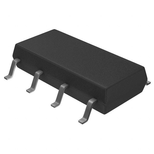
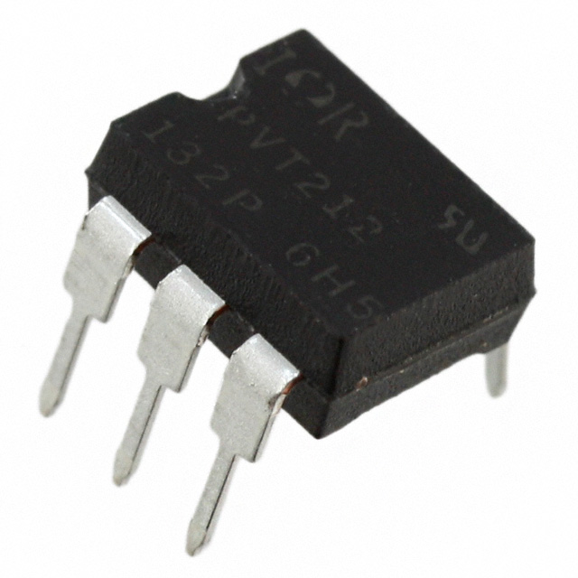
| 描述 | RELAY SSR 240VAC 2A ZC 4-SIP |
| 产品分类 | |
| 品牌 | Sharp Microelectronics |
| 数据手册 | http://www.sharpsma.com/webfm_send/311 |
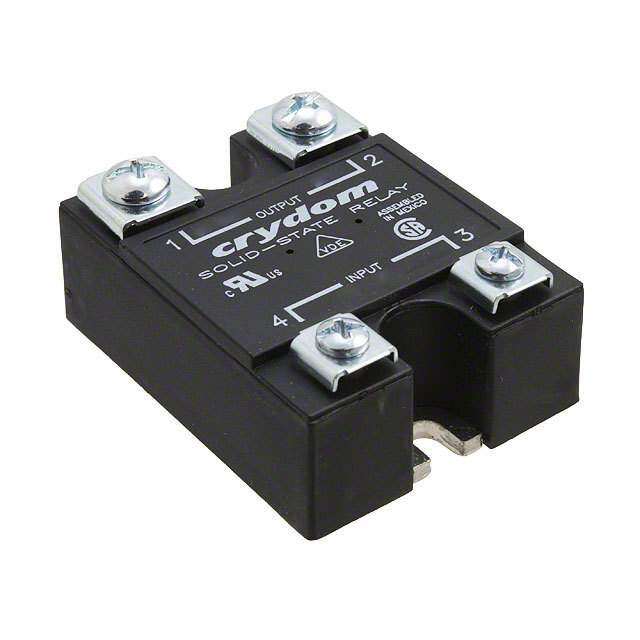
| 产品图片 |
|
| 产品型号 | S202T02F |
| rohs | 无铅 / 符合限制有害物质指令(RoHS)规范要求 |
| 产品系列 | S202 |
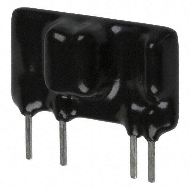
| 产品目录绘图 |
|
| 产品目录页面 | |
| 供应商器件封装 | 4-SIP |
| 其它名称 | 425-2409-5 |
| 包装 | 管件 |
| 安装类型 | 通孔 |
| 导通电阻 | - |
| 封装/外壳 | 4-SIP |
| 标准包装 | 25 |
| 电压-负载 | 80 ~ 240 V |
| 电压-输入 | 1.2VDC |
| 电路 | SPST-NO(1 A 形) |
| 端子类型 | PC 引脚 |
| 继电器类型 | |
| 负载电流 | 2A |
| 输出类型 | AC,过零 |


- 商务部:美国ITC正式对集成电路等产品启动337调查
- 曝三星4nm工艺存在良率问题 高通将骁龙8 Gen1或转产台积电
- 太阳诱电将投资9.5亿元在常州建新厂生产MLCC 预计2023年完工
- 英特尔发布欧洲新工厂建设计划 深化IDM 2.0 战略
- 台积电先进制程称霸业界 有大客户加持明年业绩稳了
- 达到5530亿美元!SIA预计今年全球半导体销售额将创下新高
- 英特尔拟将自动驾驶子公司Mobileye上市 估值或超500亿美元
- 三星加码芯片和SET,合并消费电子和移动部门,撤换高东真等 CEO
- 三星电子宣布重大人事变动 还合并消费电子和移动部门
- 海关总署:前11个月进口集成电路产品价值2.52万亿元 增长14.8%

PDF Datasheet 数据手册内容提取
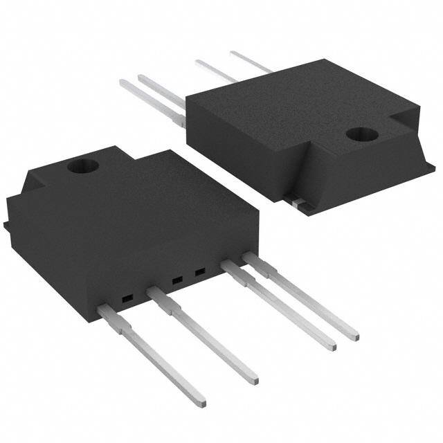
S102T02 Series S202T02 Series S102T02 Series I (rms)≤2A, Zero Cross type T Low profile SIP 4pin S202T02 Series Triac output SSR ∗Non-zero cross type is also available. (S102T01 Series/ S202T01 Series) ■ Description ■ Agency approvals/Compliance S102T02 Series and S202T02 Series Solid State 1.Recognized by UL508, file No. E94758 (as models No. Relays (SSR) are an integration of an infrared emitting S102T02/S202T02) diode (IRED), a Phototriac Detector and a main output 2. Approved by CSA 22.2 No.14, file No. LR63705 (as Triac. These devices are ideally suited for controlling models No. S102T02/S202T02) high voltage AC loads with solid state reliability while 3. Package resin : UL flammability grade (94V-0) providing 3.0kV isolation (Viso(rms)) from input to out- put. ■ Applications 1. Isolated interface between high voltage AC devices ■ Features and lower voltage DC control circuitry. 1. Output current, IT(rms)≤2.0A 2. Switching motors, fans, heaters, solenoids, and 2. Zero crossing functionary (VOX : MAX. 35V) valves. 3. Slim 4 pin low profile SIP package 3. Power control in applications such as lighting and 4. High repetitive peak off-state voltage temperature control equipment. (V : 600V, S202T02 Series) DRM (V : 400V, S102T02 Series) DRM 5. High isolation voltage between input and output (V (rms) : 3.0kV) iso 6. Lead-free terminal components are also available (see Model Line-up section in this datasheet) 7. Screw hole for heat sink NoticeThe content of data sheet is subject to change without prior notice. In the absence of confirmation by device specification sheets, SHARP takes no responsibility for any defects that may occur in equipment using any SHARP devices shown in catalogs, data books, etc. Contact SHARP in order to obtain the latest device specification sheets before using any SHARP device. Sheet No.:D4-A01601EN 1 Date Apr. 28. 2004 © SHARP Corporation
S102T02 Series S202T02 Series ■ Internal Connection Diagram 1 Output (Triac T1) 2 Output (Triac T2) 3 Input (+) 4 Input (−) 1 2 3 4 Zero Crossing Circuit ■ Outline Dimensions (Unit : mm) S102T02 S202T02 23±0.2 23±0.2 7±0.2 0.2±1.80.2±4 7±0.2 0.2±1.80.2±4 Common to pin No.2 Common to pin No.2 3±0.2 3±0.2 0.3±5 φ3.7±0.2 6.4±0.2 Common to pin No.2 0.3±5 φ3.7±0.2 6.4±0.2 Common to pin No.2 4. UL mark 4. UL mark CSA mark CSA mark Epoxy resin Epoxy resin (25.8) 0.2±11.5 S2~1A102∗25VTA0C2 + − 3D-1a.2te± 0c.2ode (2 digit) 0.2±10 (25.8) 0.2±11.5 S2~2A206∗25VTA0C2 + − 3D-1a.t2e± 0c.2ode (2 digit) 0.2±10 1.6±MIN.6.20.2 1MIN.3.8 2MIN.0.2(3.5(0.8)) 3 4 34--10..48±±00..22 0.4±0.1 (1.8) 1.6±MIN.6.20.2 1MIN.3.8 2MIN.0.2(3.5(0.8)) 3 4 34--10..48±±00..22 0.4±0.1 (1.8) 1.8±0.3 1.8±0.3 (3.8) (2.54) (3.8) (2.54) (5.08) (10.16) (5.08) (10.16) Product mass : approx. 3.5g Product mass : approx. 3.5g ∗ : Do not allow external connection. ( ) : Typical dimensions Sheet No.: D4-A01601EN 2
S102T02 Series S202T02 Series Date code (2 digit) 1st digit 2nd digit Year of production Month of production A.D. Mark A.D Mark Month Mark 1990 A 2002 P January 1 1991 B 2003 R February 2 1992 C 2004 S March 3 1993 D 2005 T April 4 1994 E 2006 U May 5 1995 F 2007 V June 6 1996 H 2008 W July 7 1997 J 2009 X August 8 1998 K 2010 A September 9 1999 L 2011 B October O 2000 M 2012 C November N · · 2001 N ·· ·· December D repeats in a 20 year cycle Country of origin Japan Rank mark There is no rank mark indicator and currently there are no rank offered for this device. Sheet No.: D4-A01601EN 3
S102T02 Series S202T02 Series ■ Absolute Maximum Ratings (T=25˚C) a Parameter Symbol Rating Unit Forward current I 50 *3 mA F Input Reverse voltage V 6 V R RMS ON-state current I (rms) 2 *3 A T Peak one cycle surge current I 20 *4 A surge Repetitive S102T02 400 VDRM V peak OFF-state voltage S202T02 600 Output Non-Repetitive S102T02 400 m VDSM V m peak OFF-state voltage S202T02 600 5 1. Critical rate of rise of ON-state current dI /dt 40 A/µs T Operating frequency f 45 to 65 Hz *1Isolation voltage V (rms) 3.0 kV iso Soldering area Operating temperature T −25 to +100 ˚C opr Storage temperature T −30 to +125 ˚C stg *2Soldering temperature T 260 ˚C sol *1 40 to 60%RH, AC for 1minute, f=60Hz *2 For 10s *3 Refer to Fig.1, Fig.2 *4 f=60Hz sine wave, Tj=25˚C start ■ Electro-optical Characteristics (T=25˚C) a Parameter Symbol Conditions MIN. TYP. MAX. Unit Forward voltage VF IF=20mA − 1.2 1.4 V Input Reverse current IR VR=3V − − 100 µA Repetitive peak OFF-state current IDRM VD=VDRM − − 100 µA ON-state voltage VT(rms) IT(rms)=2A, Resistance load, IF=20mA − − 1.7 V Output Holding current IH − − − 25 mA Critical rate of rise of OFF-state voltage dV/dt VD=2/3•VDRM 30 − − V/µs Critical rate of rise of OFF-state voltage at commutaion (dV/dt)c Tj=125˚C, VD=2/3•VDRM, dIT/dt=−1.0A/ms 4 − − V/µs Minimum trigger current IFT VD=6V, RL=30Ω − − 8 mA Zero cross voltage VOX IF=8mA − − 35 V Isolation resistance RISO DC500V, 40 to 60%RH 1010 − − Ω V (rms)=100V, AC50Hz, I =20mA D F S102T02 − − 10 Transfer Turn-on time t IT(rms)=2A, Resistance load ms on charac- V (rms)=200V, AC50Hz, I =20mA D F S202T02 − − 10 teristics I (rms)=2A, Resistance load T V (rms)=100V, AC50Hz, I =20mA D F S102T02 − − 10 I (rms)=2A, Resistance load Turn-off time t T ms off V (rms)=200V, AC50Hz, I =20mA D F S202T02 − − 10 I (rms)=2A, Resistance load T Sheet No.: D4-A01601EN 4
S102T02 Series S202T02 Series ■ Model Line-up (1) (Lead-free terminal components) Sleeve I [mA] V FT Shipping Package DRM (V =6V, D 25pcs/sleeve [V] R =30Ω) L S102T02F 400 MAX.8 Model No. S202T02F 600 MAX.8 ■ Model Line-up (2) (Lead solder plating components) Sleeve I [mA] V FT Shipping Package DRM (V =6V, D 25pcs/sleeve [V] R =30Ω) L S102T02 400 MAX.8 Model No. S202T02 600 MAX.8 Please contact a local SHARP sales representative to see the actual status of the production. Sheet No.: D4-A01601EN 5
S102T02 Series S202T02 Series Fig.1 Forward Current vs. Ambient Fig.2 RMS ON-state Current vs. Temperature Ambient Temperature 60 3.0 50 A) 2.5 A) ms) ( current I (mF 4300 e current I(rT 21..05 d at war 20 N-st 1.0 or O F S M 10 R 0.5 0 0 −25 0 25 50 75 100 125 −25 0 25 4050 75 100 125 Ambient temperature Ta (˚C) Ambient temperature Ta (˚C) Fig.3 Forward Current vs. Forward Voltage Fig.4 Surge Current vs. Power-on Cycle 100 25 f=60Hz Tj=25˚C start T=75˚C 20 a 50˚C orward current I (mA)F 101 −205˚2C˚5C˚C Surge current I (A)surge 1150 F 5 0.1 0 0.6 0.8 1.0 1.2 1.4 1.6 1.8 1 10 100 Forward voltage VF (mA) Power-on cycle (Times) Fig.5 Minimum Trigger Current vs. Fig.6 Maximum ON-state Power Dissipation Ambient Temperature vs. RMS ON-state Current 10 2.5 VD=6V W) Ta=25˚C A) 8 on ( 2 urrent I (mFT 6 wer dissipati 1.5 m trigger c 4 N-state po 1 u O m m ni u Mi 2 m 0.5 xi a M 0 0 −25 0 25 50 75 100 0 0.5 1 1.5 2 Ambient temperature T (˚C) RMS ON-state current I (rms)(A) a T Sheet No.: D4-A01601EN 6
S102T02 Series S202T02 Series Fig.7-a Repetitive Peak OFF-state Current vs. Fig.7-b Repetitive Peak OFF-state Current vs. Ambient Temperature (S102T02) Ambient Temperature (S202T02) 10−3 10−3 VD=400V VD=600V A) A) (M 10−4 (M 10−4 R R D D nt I nt I urre 10−5 urre 10−5 c c e e at at st 10−6 st 10−6 F- F- F F O O k k ea 10−7 ea 10−7 p p e e v v etiti 10−8 etiti 10−8 p p e e R R 10−9 10−9 −25 0 25 50 75 100 −25 0 25 50 75 100 Ambient temperature Ta (˚C) Ambient temperature Ta (˚C) Remarks : Please be aware that all data in the graph are just for reference. Sheet No.: D4-A01601EN 7
S102T02 Series S202T02 Series ■ Design Considerations ● Recommended Operating Conditions Parameter Symbol Conditions MIN. MAX. Unit Input signal current at ON state IF(ON) − 16 24 mA Input Input signal current at OFF state IF(OFF) − 0 0.1 mA S102T02 80 120 Load supply voltage S202T02 VOUT(rms) − 80 240 V Output Locate snubber circuit between output terminals I (rms) Load supply current I (rms) 0.1 T mA OUT (Cs=0.022µF, Rs=47Ω) ×80%(∗) Frequency f − 47 63 Hz Operating temperature Topr − −20 80 ˚C (∗) See Fig.2 about derating curve (I(rms) vs. ambient temperature). T ● Design guide In order for the SSR to turn off, the triggering current (l ) must be 0.1mA or less. F When the input current (I ) is below 0.1mA, the output Triac will be in the open circuit mode. However, if the F voltage across the Triac, V , increases faster than rated dV/dt, the Triac may turn on. To avoid this situation, D please incorporate a snubber circuit. Due to the many different types of load that can be driven, we can merely recommend some circuit vales to start with : Cs=0.022µF and Rs=47Ω. The operation of the SSR and snubber circuit should be tested and if unintentional switching occurs, please adjust the snubber circuit component values accordingly. When making the transition from On to Off state, a snubber circuit should be used ensure that sudden drops in current are not accompanied by large instantaneous changes in voltage across the Triac. This fast change in voltage is brought about by the phase difference between current and voltage. Primarily, this is experienced in driving loads which are inductive such as motors and solenoids. Following the procedure outlined above should provide sufficient results. For over voltage protection, a Varistor may be used. Any snubber or Varistor used for the above mentioned scenarios should be located as close to the main out- put triac as possible. Particular attention needs to be paid when utilizing SSRs that incorporate zero crossing circuitry. If the phase difference between the voltage and the current at the output pins is large enough, zero crossing type SSRs cannot be used. The result, if zero crossing SSRs are used under this condition, is that the SSR may not turn on and off irregardless of the input current. In this case, only a non zero cross type SSR should be used in combination with the above mentioned snubber circuit selection process. The load current should be within the bounds of derating curve. (Refer to Fig.2) Also, please use the optional heat sink when necessary. In case the optional heat sink is used and the isolation voltage between the device and the optional heat sink is needed, please locate the insulation sheet between the device and the heat sink. When the optional heat sink is equipped, please set up the M3 screw-fastening torque at 0.3 to 0.5N•m. In order to dissipate the heat generated from the inside of device effectively, please follow the below sugges- tions. Sheet No.: D4-A01601EN 8
S102T02 Series S202T02 Series (a) Make sure there are no warps or bumps on the heat sink, insulation sheet and device surface. (b) Make sure there are no metal dusts or burrs attached onto the heat sink, insulation sheet and device sur- face. (c) Make sure silicone grease is evenly spread out on the heat sink, insulation sheet and device surface. Silicone grease to be used is as follows; 1) There is no aged deterioration within the operating temperature ranges. 2) Base oil of grease is hardly separated and is hardly permeated in the device. 3) Even if base oil is separated and permeated in the device, it should not degrade the function of a device. Recommended grease: G-746 (Shin-Etsu Chemical Co., Ltd.) : G-747 (Shin-Etsu Chemical Co., Ltd.) : SC102 (Dow Corning Toray Silicone Co., Ltd.) In case the optional heat sink is screwed up, please solder after screwed. In case of the lead frame bending, please keep the following minimum distance and avoid any mechanical stress between the base of terminals and the molding resin. 3.8mm MIN. Some of AC electromagnetic counters or solenoids have built-in rectifier such as the diode. In this case, please use the device carefully since the load current waveform becomes similar with rectangu- lar waveform and this results may not make a device turn off. ● Degradation In general, the emission of the IRED used in SSR will degrade over time. In the case where long term operation and / or constant extreme temperature fluctuations will be applied to the devices, please allow for a worst case scenario of 50% degradation over 5years. Therefore in order to maintain proper operation, a design implementing these SSRs should provide at least twice the minimum required triggering current from initial operation. ● Standard Circuit S102T02 S202T02 R 1 +VCC 3 2 Load D SSR Z 1 S AC Line V 4 1 1 Tr1 Z : Surge absorption circuit (Snubber circuit) S ✩ For additional design assistance, please review our corresponding Optoelectronic Application Notes. Sheet No.: D4-A01601EN 9
S102T02 Series S202T02 Series ■ Manufacturing Guidelines ● Soldering Method Flow Soldering (No solder bathing) Flow soldering should be completed below 260˚C and within 10s. Preheating is within the bounds of 100 to 150˚C and 30 to 80s. Please solder within one time. Other notices Please test the soldering method in actual condition and make sure the soldering works fine, since the impact on the junction between the device and PCB varies depending on the tooling and soldering conditions. Sheet No.: D4-A01601EN 10
S102T02 Series S202T02 Series ● Cleaning instructions Solvent cleaning : Solvent temperature should be 45˚C or below. Immersion time should be 3minutes or less. Ultrasonic cleaning : The impact on the device varies depending on the size of the cleaning bath, ultrasonic output, cleaning time, size of PCB and mounting method of the device. Therefore, please make sure the device withstands the ultrasonic cleaning in actual conditions in advance of mass production. Recommended solvent materials : Ethyl alcohol, Methyl alcohol and Isopropyl alcohol. In case the other type of solvent materials are intended to be used, please make sure they work fine in ac- tual using conditions since some materials may erode the packaging resin. ● Presence of ODC This product shall not contain the following materials. And they are not used in the production process for this device. Regulation substances : CFCs, Halon, Carbon tetrachloride, 1.1.1-Trichloroethane (Methylchloroform) Specific brominated flame retardants such as the PBBOs and PBBs are not used in this product at all. Sheet No.: D4-A01601EN 11
S102T02 Series S202T02 Series ■ Package specification ● Sleeve package Package materials Sleeve : HIPS Stopper : Olefine-Elastomer Package method MAX. 25pcs of products shall be packaged in a sleeve. Both ends shall be closed by stoppers. MAX. 20 sleeves in one case. Sleeve outline dimensions 8 620±2 11..11 12.0 17. 0.0) 3 ( 6 0. 1 4.7 7.6 (8.5) (Unit : mm) Sheet No.: D4-A01601EN 12
S102T02 Series S202T02 Series ■ Important Notices · The circuit application examples in this publication are with equipment that requires higher reliability such as: provided to explain representative applications of --- Transportation control and safety equipment (i.e., SHARP devices and are not intended to guarantee any aircraft, trains, automobiles, etc.) circuit design or license any intellectual property rights. --- Traffic signals SHARP takes no responsibility for any problems rela- --- Gas leakage sensor breakers ted to any intellectual property right of a third party re- --- Alarm equipment sulting from the use of SHARP's devices. --- Various safety devices, etc. (iii) SHARP devices shall not be used for or in connec- · Contact SHARP in order to obtain the latest device tion with equipment that requires an extremely high lev- specification sheets before using any SHARP device. el of reliability and safety such as: SHARP reserves the right to make changes in the spec- --- Space applications ifications, characteristics, data, materials, structure, --- Telecommunication equipment [trunk lines] and other contents described herein at any time without --- Nuclear power control equipment notice in order to improve design or reliability. Manufac- --- Medical and other life support equipment (e.g., turing locations are also subject to change without no- scuba). tice. · If the SHARP devices listed in this publication fall with- · Observe the following points when using any devices in the scope of strategic products described in the For- in this publication. SHARP takes no responsibility for eign Exchange and Foreign Trade Law of Japan, it is damage caused by improper use of the devices which necessary to obtain approval to export such SHARP de- does not meet the conditions and absolute maximum vices. ratings to be used specified in the relevant specification sheet nor meet the following conditions: · This publication is the proprietary product of SHARP (i) The devices in this publication are designed for use and is copyrighted, with all rights reserved. Under the in general electronic equipment designs such as: copyright laws, no part of this publication may be repro- --- Personal computers duced or transmitted in any form or by any means, elec- --- Office automation equipment tronic or mechanical, for any purpose, in whole or in --- Telecommunication equipment [terminal] part, without the express written permission of SHARP. --- Test and measurement equipment Express written permission is also required before any --- Industrial control use of this publication may be made by a third party. --- Audio visual equipment --- Consumer electronics · Contact and consult with a SHARP representative if (ii) Measures such as fail-safe function and redundant there are any questions about the contents of this pub- design should be taken to ensure reliability and safety lication. when SHARP devices are used for or in connection Sheet No.: D4-A01601EN 13