ICGOO在线商城 > 集成电路(IC) > PMIC - 电源管理 - 专用 > RV4145AN

 Datasheet下载
- 型号: RV4145AN
- 制造商: Fairchild Semiconductor
- 库位|库存: xxxx|xxxx
- 要求:
| 数量阶梯 | 香港交货 | 国内含税 |
| +xxxx | $xxxx | ¥xxxx |
查看当月历史价格
查看今年历史价格
RV4145AN产品简介:
ICGOO电子元器件商城为您提供RV4145AN由Fairchild Semiconductor设计生产,在icgoo商城现货销售,并且可以通过原厂、代理商等渠道进行代购。 RV4145AN价格参考¥2.47-¥2.47。Fairchild SemiconductorRV4145AN封装/规格:PMIC - 电源管理 - 专用, Ground Fault Protection PMIC 8-DIP。您可以下载RV4145AN参考资料、Datasheet数据手册功能说明书,资料中有RV4145AN 详细功能的应用电路图电压和使用方法及教程。
ON Semiconductor的RV4145AN是一款专用电源管理集成电路(PMIC),主要应用于需要高效、稳定电源管理的便携式和低功耗设备。以下是其典型应用场景:

1. 可穿戴设备:如智能手表、健身追踪器等,RV4145AN能够提供高效的电源转换和管理功能,延长电池续航时间,同时支持小型化设计。

2. 物联网(IoT)设备:包括智能家居传感器、环境监测设备等。该芯片可以为低功耗的IoT节点提供稳定的电源供应,并优化能量使用。

3. 便携式医疗设备:例如血糖仪、脉搏血氧仪等。RV4145AN能够确保设备在电池供电的情况下保持高性能和精确性。

4. 移动通信设备:如蓝牙耳机、无线鼠标、键盘等。它支持多种电压输出配置,适应不同模块(如处理器、存储器、传感器)的供电需求。

5. 手持消费电子产品:例如电子书阅读器、数码相机等。通过集成多路电源轨,RV4145AN简化了系统设计并提高了效率。

6. 工业自动化模块:用于无线传感器网络或远程监控单元中,提供可靠的电源管理和保护功能。

RV4145AN的特点使其非常适合对尺寸敏感且要求长电池寿命的应用场合,同时它的灵活性允许开发者根据具体需求调整电源设置。
| 参数 | 数值 |
| 产品目录 | 集成电路 (IC)半导体 |
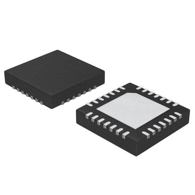
| 描述 | IC CTRLR LP AC GFI 8-DIP电流和电力监控器、调节器 Low Pwr Ground Fault Interrupt Cont |
| 产品分类 | |
| 品牌 | Fairchild Semiconductor |
| 产品手册 | |
| 产品图片 |
|
| rohs | 符合RoHS无铅 / 符合限制有害物质指令(RoHS)规范要求 |
| 产品系列 | 电源管理 IC,电流和电力监控器、调节器,Fairchild Semiconductor RV4145AN- |
| 数据手册 | |
| 产品型号 | RV4145AN |
| PCN封装 | |
| PCN设计/规格 | |
| 产品 | Current and Power Monitors |
| 产品种类 | 电流和电力监控器、调节器 |
| 供应商器件封装 | 8-DIP |
| 其它名称 | RV4145AN-ND |
| 包装 | 管件 |
| 单位重量 | 851 mg |
| 商标 | Fairchild Semiconductor |
| 安装类型 | 通孔 |
| 安装风格 | Through Hole |
| 封装 | Tube |
| 封装/外壳 | 8-DIP(0.300",7.62mm) |
| 封装/箱体 | PDIP-8 |
| 工作温度 | -35°C ~ 85°C |
| 工作温度范围 | - 35 C to + 85 C |
| 工厂包装数量 | 40 |
| 应用 | 接地故障保护 |
| 标准包装 | 40 |
| 电压-电源 | - |
| 电流-电源 | 18mA |
| 电源电压-最大 | 29.2 V |
| 电源电压-最小 | 25 V |
| 电源电流 | 18 mA |
| 系列 | RV4145A |
| 输入电压范围 | 25 V to 29.2 V |
| 零件号别名 | RV4145AN_NL |


- 商务部:美国ITC正式对集成电路等产品启动337调查
- 曝三星4nm工艺存在良率问题 高通将骁龙8 Gen1或转产台积电
- 太阳诱电将投资9.5亿元在常州建新厂生产MLCC 预计2023年完工
- 英特尔发布欧洲新工厂建设计划 深化IDM 2.0 战略
- 台积电先进制程称霸业界 有大客户加持明年业绩稳了
- 达到5530亿美元!SIA预计今年全球半导体销售额将创下新高
- 英特尔拟将自动驾驶子公司Mobileye上市 估值或超500亿美元
- 三星加码芯片和SET,合并消费电子和移动部门,撤换高东真等 CEO
- 三星电子宣布重大人事变动 还合并消费电子和移动部门
- 海关总署:前11个月进口集成电路产品价值2.52万亿元 增长14.8%


PDF Datasheet 数据手册内容提取
Is Now Part of To learn more about ON Semiconductor, please visit our website at www.onsemi.com Please note: As part of the Fairchild Semiconductor integration, some of the Fairchild orderable part numbers will need to change in order to meet ON Semiconductor’s system requirements. Since the ON Semiconductor product management systems do not have the ability to manage part nomenclature that utilizes an underscore (_), the underscore (_) in the Fairchild part numbers will be changed to a dash (-). This document may contain device numbers with an underscore (_). Please check the ON Semiconductor website to verify the updated device numbers. The most current and up-to-date ordering information can be found at www.onsemi.com. Please email any questions regarding the system integration to Fairchild_questions@onsemi.com. ON Semiconductor and the ON Semiconductor logo are trademarks of Semiconductor Components Industries, LLC dba ON Semiconductor or its subsidiaries in the United States and/or other countries. ON Semiconductor owns the rights to a number of patents, trademarks, copyrights, trade secrets, and other intellectual property. A listing of ON Semiconductor’s product/patent coverage may be accessed at www.onsemi.com/site/pdf/Patent-Marking.pdf. ON Semiconductor reserves the right to make changes without further notice to any products herein. ON Semiconductor makes no warranty, representation or guarantee regarding the suitability of its products for any particular purpose, nor does ON Semiconductor assume any liability arising out of the application or use of any product or circuit, and specifically disclaims any and all liability, including without limitation special, consequential or incidental damages. Buyer is responsible for its products and applications using ON Semiconductor products, including compliance with all laws, regulations and safety requirements or standards, regardless of any support or applications information provided by ON Semiconductor. “Typical” parameters which may be provided in ON Semiconductor data sheets and/or specifications can and do vary in different applications and actual performance may vary over time. All operating parameters, including “Typicals” must be validated for each customer application by customer’s technical experts. ON Semiconductor does not convey any license under its patent rights nor the rights of others. ON Semiconductor products are not designed, intended, or authorized for use as a critical component in life support systems or any FDA Class 3 medical devices or medical devices with a same or similar classification in a foreign jurisdiction or any devices intended for implantation in the human body. Should Buyer purchase or use ON Semiconductor products for any such unintended or unauthorized application, Buyer shall indemnify and hold ON Semiconductor and its officers, employees, subsidiaries, affiliates, and distributors harmless against all claims, costs, damages, and expenses, and reasonable attorney fees arising out of, directly or indirectly, any claim of personal injury or death associated with such unintended or unauthorized use, even if such claim alleges that ON Semiconductor was negligent regarding the design or manufacture of the part. ON Semiconductor is an Equal Opportunity/Affirmative Action Employer. This literature is subject to all applicable copyright laws and is not for resale in any manner.
R V 4 1 4 April 2014 5 A — L o w P o RV4145A — Low-Power Ground Fault Interrupter w e r G r o u n Features Description d F No Potentiometer Required The RV4145A is a low-power controller for AC outlet au ground fault interrupters. These devices detect l Direct Interface to Silicon-Controlled Rectifier (SCR) hazardous grounding conditions, such as equipment t I n Supply Voltage Derived from AC Line – 26 V Shunt (connected to opposite phases of the AC line) in contact t with a pool of water and open circuits the line before a e Adjustable Sensitivity harmful or lethal shock occurs. rr u Grounded Neutral Fault Detection A 26 V Zener shunt regulator, an operational amplifier, pt e Meets U.L. 943 Standards and an SCR driver are contained internally. With the r addition of two sense transformers, a bridge rectifier, an 450 μA Quiescent Current SCR, a relay, and a few additional components; the Ideal for 120 V or 220 V Systems RV4145A can detect and protect against both hot-wire- to-ground and neutral-wire-to-ground faults. The simple layout and conventional design ensure ease of application and long-term reliability. Figure 1. Block Diagram Ordering Information Operating Part Number Package Packing Method Temperature Range RV4145AN 8-Lead, MDIP, JEDEC MS-001, .300" Wide Rail -35°C to +85°C RV4145AMT 8-Lead, SOIC, JEDEC MS-012, .150" Narrow Body Tape and Reel © 2004 Fairchild Semiconductor Corporation www.fairchildsemi.com GPN • Rev. 1.0.6
R V 4 1 4 Pin Configuration 5 A — L o w P o w e r G r o u Figure 2. Pin Assignment n d F a u l t Pin Descriptions I n t e Pin# Name Description r r u 1 VFB Sense amplifier negative input p t 2 +Input Sense amplifier positive input e r 3 V Reference Voltage REF 4 GND Ground 5 NC No Connect 6 Op Amp Output Sense Amplifier Output 7 +V Supply input for RV4145A circuitry S 8 SCR Trigger Output for triggering external SCR when a fault is detected © 2004 Fairchild Semiconductor Corporation www.fairchildsemi.com RV4145A • Rev. 1.0.6 2
R V 4 1 4 5 A Absolute Maximum Ratings — L Stresses exceeding the absolute maximum ratings may damage the device. The device may not function or be o operable above the recommended operating conditions and stressing the parts to these levels is not recommended. w In addition, extended exposure to stresses above the recommended operating conditions may affect device reliability. P The absolute maximum ratings are stress ratings only. o w e Symbol Parameter Min. Typ. Max. Unit r G V Supply Current 18 mA CC r o PD Internal Power Dissipation 500 mW u n TSTG Storage Temperature Range -65 +150 °C d F T Operating Temperature Range -35 +85 °C A a u TJ Junction Temperature 125 °C lt 60 s, DIP 300 In TL Lead Soldering Temperature 10 s, SOIC 260 °C te r r SOIC 300 u T <50°C mW p A PDIP 450 t e PD Power Dissipation r SOIC 4 T <50°C Derate mW/°C A PDIP 6 SOIC 240 Thermal Resistance °C/W JA PDIP 160 © 2004 Fairchild Semiconductor Corporation www.fairchildsemi.com RV4145A • Rev. 1.0.6 3
R V 4 1 4 Electrical Characteristics 5 A I = 1.5 mA and T = +25°C. — S A L Symbol Parameter Conditions Min. Typ. Max. Unit o w Detector Reference Voltage Pin 7 to Pin 3 6.8 7.2 8.1 ±V P Shunt Regulator o w +VS Zener Voltage Pin 6 to Pin 4 25.0 26.0 29.2 V e r VREF Reference Voltage Pin 3 to Pin 4 12.5 13.0 14.6 V G Is Quiescent Current +VS = 24 V 450 750 µA ro u Operation Amplifier n d Offset Voltage Pin 2 to Pin 3 -3.0 0.5 +3.0 mV F +Output Voltage Swing Pin 7 to Pin 3 6.8 7.2 8.1 V a u -Output Voltage Swing Pin 7 to Pin 3 -9.5 -11.2 -13.5 V l t +Output Source Current Pin 7 to Pin 3 650 µA In t -Output Source Current Pin 7 to Pin 3 1.0 mA e r r Gain Bandwidth Product f = 50 kHz 1.0 1.8 MHz u p Resistors t e R1 Pin 1 to Pin 3 10 r R2 Resistors, I = 0 mA Pin 2 to Pin 3 10 k S R3 Pin 5 to Pin 4 3.5 4.7 5.9 SCR Trigger Detector On 1.5 2.8 V Pin 5 to Pin 4 Detector Off 0 1 10 mV Electrical Characteristics I = 1.5 mA and -35°C ≤ T ≤ +85°C. S A Symbol Parameter Conditions Min. Typ. Max. Unit Detector Reference Voltage Pin 7 to Pin 3 6.5 7.2 8.3 ±V Shunt Regulator +V Zener Voltage Pin 6 to Pin 4 24 26 30 V S V Reference Voltage Pin 3 to Pin 4 12 13 15 V REF I Quiescent Current +V = 23 V 500 µA S S Operational Amplifier Offset Voltage Pin 2 to Pin 3 -5.0 0.5 +5.0 mV +Output Voltage Swing Pin 7 to Pin 3 6.5 7.2 8.3 V -Output Voltage Swing Pin 7 to Pin 3 -9.0 -11.2 -14.0 V Gain Bandwidth Product f = 50 kHz 1.8 MHz Resistors R1 Pin 1 to Pin 3 10 R2 Resistors, IS = 0 mA Pin 2 to Pin 3 10 k R3 Pin 5 to Pin 4 3.5 4.7 5.9 SCR Trigger Detector On 1.3 2.8 V Pin 5 to Pin 4 Detector Off 0 3 50 mV © 2004 Fairchild Semiconductor Corporation www.fairchildsemi.com RV4145A • Rev. 1.0.6 4
R V 4 1 Principles of Operation 4 5 A The 26 V shunt regulator voltage generated by the Silicon-Controlled Rectifier (SCR) Driver string of Zener diodes is divided into three reference — The SCR must have a high dV/dt rating to ensure that voltages: ¾ V , ½ V , and ¼ V . V is at ½ V and is S S S REF S line noise (generated by noisy appliances, such as a L used as a reference to create an artificial ground of o +13 V at the operational amplifier non-inverting input. drill motor) does not falsely trigger the SCR. The SCR w must have a gate-drive requirement of less than 200 μA. P Figure 3 shows a three-wire 120 V AC outlet GFI CF is a noise filter capacitor that prevents narrow pulses o application using an RV4145A. Fault signals from the from firing the SCR. w sense transformer are AC coupled into the input and are e The relay solenoid should have a 3 ms or less response r amplified according to the following equation: G time to meet the UL 943 timing requirement. r o (1) Sense Transformers and Cores u n where V is the RMS voltage at pin 7 relative to pin 3, The sense and grounded neutral transformer cores are d 7 R is the value of the feedback resistor connected usually fabricated using high permeability laminated F SENSE from pin 7 to pin 1, I is the fault current (in amps) steel rings. Their single-turn primary is created by a SENSE u RMS, and N is the turns ratio of the transformer. passing the line and neutral wires through the center of l t the core. The secondary is usually 200 to 1500 turns. I When V exceeds ±7.2 V relative to pin 3, the SCR n 7 t trigger output goes high and fires the external SCR. Magnetic Metals Corporation www.magmet.com is a full e r line suppliers of ring cores and transformers designed r The formula for V7 is approximate because it does not specifically for GFI applications. up include the sense transformer characteristics. t Two-Wire Application Circuit e r Grounded neutral fault detection is accomplished when a short or fault closes a magnetic path between the Figure 4 shows the diagram of a two-wire 120 V AC sense transformer and the grounded neutral outlet GFI circuit using an RV4145A. This circuit is not transformer. The resultant AC coupling closes a positive designed to detect grounded neutral faults. For this feedback path around the op amp, and the op amp reason, the grounded neutral transformer and oscillates. When the peaks of the oscillation voltage capacitors C3 and C4 of Figure 3 are not used. exceed the SCR trigger comparator thresholds, the SCR output goes high. Shunt Regulator The R limits the current into the shunt regulator; LINE 220 V applications must substitute a 47 k 2 W resistor. In addition to supplying power to the IC, the shunt regulator creates internal reference voltages. Operational Amplifier R is a feedback resistor that sets gain and, SENSE therefore sensitivity to normal faults. To adjust R , SENSE apply the desired fault current (a difference in current of 5 mA is the UL 943 standard) then adjust R upward SENSE until the SCR activates. A fixed resistor can be used for R because the resultant ±15% variation in SENSE sensitivity meets UL’s 943 4-6 mA specification window. The roll-off frequency is greater than the grounded neutral fault oscillation frequency to preserve loop gain for oscillation (which is determined by the inductance of the 200:1 transformer and C4). The sensitivity to grounded neutral faults is adjusted by changing the frequency of oscillation. Increasing the frequency reduces the sensitivity by reducing the loop gain of the positive feedback circuit. As frequency increases, the signal becomes attenuated and the loop gain decreases. With the values shown in Figure 3, the circuit detects a grounded neutral with resistance of 2 Ω or less. The input to the operational amplifier is protected from over-voltage by back-to-back diodes. © 2004 Fairchild Semiconductor Corporation www.fairchildsemi.com RV4145A • Rev. 1.0.6 5
R V 4 1 4 5 A — L o w P o w e r G r o u n d F a u l t I n t e r r u p t e r Figure 3. GFI Application Circuit (Three-Wire Outlet) Figure 4. GFI Application Circuit (Two-Wire Outlet) © 2004 Fairchild Semiconductor Corporation www.fairchildsemi.com RV4145A • Rev. 1.0.6 6
R V 4 1 4 Schematic Diagram 5 A — L o w P o w e r G r o u n d F a u l t I n t e r r u p t e r Figure 5. Schematic © 2004 Fairchild Semiconductor Corporation www.fairchildsemi.com RV4145A • Rev. 1.0.6 7
R V 4 1 4 Physical Dimensions 5 A — .400[10.15] A .373 9.46 L o w .036 [0.9 TYP] P o (.092) [Ø2.337] w e PIN #1 (.032) [R0.813] r .250±.005 [6.35±0.13] G PIN #1 r o u n d B TOP VIEW TOP VIEW F OPTION 1 OPTION 2 a u l ..007405 [11..7184] .310±.010 [7.87±0.25] t In t .130±.005 [3.3±0.13] e 7° TYP .210 MAX rr [5.33] u p 7° TYP t e r C .015 MIN .021[0.53] [0.38] .015 0.37 .140[3.55] .300 .125 3.17 [7.62] .001[.025] C .100 .430 MAX [2.54] [10.92] NOTES: .060 MAX [1.52] A. CONFORMS TO JEDEC REGISTRATION MS-001, +.005[ +0.127] VARIATIONS BA .010-.000 0.254-0.000 B. CONTROLING DIMENSIONS ARE IN INCHES REFERENCE DIMENSIONS ARE IN MILLIMETERS C. DOES NOT INCLUDE MOLD FLASH OR PROTRUSIONS. MOLD FLASH OR PROTRUSIONS SHALL NOT EXCEED .010 INCHES OR 0.25MM. D. DOES NOT INCLUDE DAMBAR PROTRUSIONS. DAMBAR PROTRUSIONS SHALL NOT EXCEED .010 INCHES OR 0.25MM. E. DIMENSIONING AND TOLERANCING PER ASME Y14.5M-1994. N08EREVG Figure 6. 8-Lead, MDIP, JEDEC MS-001, .300" Wide Package drawings are provided as a service to customers considering Fairchild components. Drawings may change in any manner without notice. Please note the revision and/or date on the drawing and contact a Fairchild Semiconductor representative to verify or obtain the most recent revision. Package specifications do not expand the terms of Fairchild’s worldwide terms and conditions, specifically the warranty therein, which covers Fairchild products. Always visit Fairchild Semiconductor’s online packaging area for the most recent package drawings: http://www.fairchildsemi.com/ dwg/N0/N08E.pdf For current packing container specifications, visit Fairchild Semiconductor’s online packaging area: http://www.fairchildsemi.com/packing_dwg/PKG-N08E.pdf © 2004 Fairchild Semiconductor Corporation www.fairchildsemi.com RV4145A • Rev. 1.0.6 8
R V 4 1 4 Physical Dimensions 5 A — 0.65 L o 4.90±0.10 A w (0.635) P 8 5 o B w e r 1.75 G 6.00±0.20 r 3.90±0.10 5.60 ou n d F a u PIN ONE 1 4 lt I INDICATOR 1.27 n t 1.27 e r 0.25 C B A LAND PATTERN RECOMMENDATION r u p SEE DETAIL A te 0.175±0.075 r 0.22±0.30 1.75 MAX C 0.10 0.42±0.09 OPTION A - BEVEL EDGE (0.86) x 45° R0.10 GAGE PLANE R0.10 OPTION B - NO BEVEL EDGE 0.36 8° NOTES: UNLESS OTHERWISE SPECIFIED 0° A) THIS PACKAGE CONFORMS TO JEDEC MS-012, VARIATION AA. SEATING PLANE B) ALL DIMENSIONS ARE IN MILLIMETERS. 0.65±0.25 C) DIMENSIONS DO NOT INCLUDE MOLD (1.04) FLASH OR BURRS. D) LANDPATTERN STANDARD: SOIC127P600X175-8M. DETAIL A E) DRAWING FILENAME: M08Arev15 SCALE: 2:1 F) FAIRCHILD SEMICONDUCTOR. Figure 7. 8-Lead, SOIC, JEDEC MS-012, .150" Narrow Body Package drawings are provided as a service to customers considering Fairchild components. Drawings may change in any manner without notice. Please note the revision and/or date on the drawing and contact a Fairchild Semiconductor representative to verify or obtain the most recent revision. Package specifications do not expand the terms of Fairchild’s worldwide terms and conditions, specifically the warranty therein, which covers Fairchild products. Always visit Fairchild Semiconductor’s online packaging area for the most recent package drawings: http://www.fairchildsemi.com/ dwg/M0/M08A.pdf For current packing container specifications, visit Fairchild Semiconductor’s online packaging area: http://www.fairchildsemi.com/packing_dwg/PKG-M08A_GEM.pdf © 2004 Fairchild Semiconductor Corporation www.fairchildsemi.com RV4145A • Rev. 1.0.6 9
R V 4 1 4 5 A — L o w P o w e r G r o u n d F a u l t I n t e r r u p t e r © 2004 Fairchild Semiconductor Corporation www.fairchildsemi.com RV4145A • Rev. 1.0.6 10
ON Semiconductor and are trademarks of Semiconductor Components Industries, LLC dba ON Semiconductor or its subsidiaries in the United States and/or other countries. ON Semiconductor owns the rights to a number of patents, trademarks, copyrights, trade secrets, and other intellectual property. A listing of ON Semiconductor’s product/patent coverage may be accessed at www.onsemi.com/site/pdf/Patent−Marking.pdf. ON Semiconductor reserves the right to make changes without further notice to any products herein. ON Semiconductor makes no warranty, representation or guarantee regarding the suitability of its products for any particular purpose, nor does ON Semiconductor assume any liability arising out of the application or use of any product or circuit, and specifically disclaims any and all liability, including without limitation special, consequential or incidental damages. Buyer is responsible for its products and applications using ON Semiconductor products, including compliance with all laws, regulations and safety requirements or standards, regardless of any support or applications information provided by ON Semiconductor. “Typical” parameters which may be provided in ON Semiconductor data sheets and/or specifications can and do vary in different applications and actual performance may vary over time. All operating parameters, including “Typicals” must be validated for each customer application by customer’s technical experts. ON Semiconductor does not convey any license under its patent rights nor the rights of others. ON Semiconductor products are not designed, intended, or authorized for use as a critical component in life support systems or any FDA Class 3 medical devices or medical devices with a same or similar classification in a foreign jurisdiction or any devices intended for implantation in the human body. Should Buyer purchase or use ON Semiconductor products for any such unintended or unauthorized application, Buyer shall indemnify and hold ON Semiconductor and its officers, employees, subsidiaries, affiliates, and distributors harmless against all claims, costs, damages, and expenses, and reasonable attorney fees arising out of, directly or indirectly, any claim of personal injury or death associated with such unintended or unauthorized use, even if such claim alleges that ON Semiconductor was negligent regarding the design or manufacture of the part. ON Semiconductor is an Equal Opportunity/Affirmative Action Employer. This literature is subject to all applicable copyright laws and is not for resale in any manner. PUBLICATION ORDERING INFORMATION LITERATURE FULFILLMENT: N. American Technical Support: 800−282−9855 Toll Free ON Semiconductor Website: www.onsemi.com Literature Distribution Center for ON Semiconductor USA/Canada 19521 E. 32nd Pkwy, Aurora, Colorado 80011 USA Europe, Middle East and Africa Technical Support: Order Literature: http://www.onsemi.com/orderlit Phone: 303−675−2175 or 800−344−3860 Toll Free USA/Canada Phone: 421 33 790 2910 Fax: 303−675−2176 or 800−344−3867 Toll Free USA/Canada Japan Customer Focus Center For additional information, please contact your local Email: orderlit@onsemi.com Phone: 81−3−5817−1050 Sales Representative © Semiconductor Components Industries, LLC www.onsemi.com www.onsemi.com 1
Mouser Electronics Authorized Distributor Click to View Pricing, Inventory, Delivery & Lifecycle Information: O N Semiconductor: RV4145AMT RV4145AN