ICGOO在线商城 > 集成电路(IC) > PMIC - 稳压器 - DC DC 开关稳压器 > RT8082GQW
 Datasheet下载
- 型号: RT8082GQW
- 制造商: RICHTEK
- 库位|库存: xxxx|xxxx
- 要求:
| 数量阶梯 | 香港交货 | 国内含税 |
| +xxxx | $xxxx | ¥xxxx |
查看当月历史价格
查看今年历史价格
RT8082GQW产品简介:
ICGOO电子元器件商城为您提供RT8082GQW由RICHTEK设计生产,在icgoo商城现货销售,并且可以通过原厂、代理商等渠道进行代购。 RT8082GQW价格参考。RICHTEKRT8082GQW封装/规格:PMIC - 稳压器 - DC DC 开关稳压器, 可调式 降压 开关稳压器 IC 正 1V 1 输出 3A 12-WFDFN 裸露焊盘。您可以下载RT8082GQW参考资料、Datasheet数据手册功能说明书,资料中有RT8082GQW 详细功能的应用电路图电压和使用方法及教程。
RT8082GQW 是 Richtek(立锜科技)生产的一款 PMIC(电源管理集成电路),属于 DC-DC 开关稳压器类别。其主要应用场景包括但不限于以下领域:

1. 便携式电子设备:
   RT8082GQW 适用于需要高效电源转换的便携式设备,例如智能手机、平板电脑、可穿戴设备(如智能手表和健康监测器)。它具有低功耗特性,能够延长电池寿命,同时支持稳定的电压输出以驱动各种负载。

2. 消费类电子产品:
   该芯片可用于电视、机顶盒、游戏机和其他消费类电子产品中,为内部电路提供高效的电源管理。其高集成度和小封装设计非常适合对空间要求严格的消费类产品。

3. 通信设备:
   在路由器、调制解调器、Wi-Fi 设备等通信产品中,RT8082GQW 可以作为核心电源模块,为处理器、存储器和其他关键组件供电,确保系统稳定运行。

4. 工业控制与自动化:
   RT8082GQW 的高效率和可靠性使其成为工业控制设备的理想选择,例如 PLC(可编程逻辑控制器)、传感器接口模块以及数据采集系统。这些应用通常需要在较宽的工作温度范围内保持性能稳定。

5. 汽车电子:
   尽管 RT8082GQW 并非专为汽车级设计,但在某些非关键车载应用中(如信息娱乐系统或导航模块),它也可以发挥作用,提供稳定的电源支持。

6. 物联网 (IoT) 设备:
   在智能家居、环境监测和其他 IoT 应用中,RT8082GQW 的低静态电流和高效率特性非常适合为微控制器、无线模块和传感器供电。

7. 网络与存储设备:
   该芯片可用于网络交换机、NAS(网络附加存储)设备以及其他数据中心相关硬件中,为系统提供可靠的电源解决方案。

总结来说,RT8082GQW 凭借其高效的电源转换能力、紧凑的封装尺寸和良好的稳定性,广泛应用于各类需要高性能电源管理的场景,尤其是在注重能效和小型化的现代电子产品中。
| 参数 | 数值 |
| 产品目录 | 集成电路 (IC) |
| 描述 | IC REG BUCK SYNC ADJ 3A 12WDFN |
| 产品分类 | |
| 品牌 | Richtek USA Inc |
| 数据手册 | http://www.richtek.com/download_ds.jsp?s=945 |
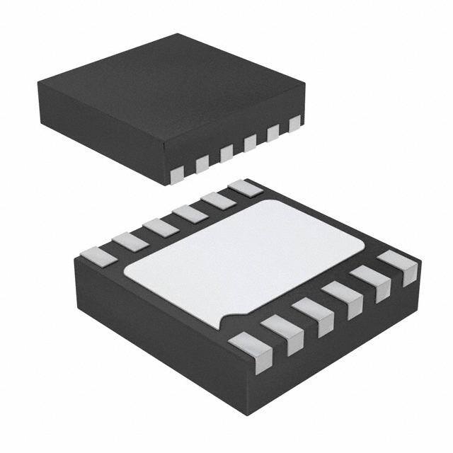
| 产品图片 |
|
| 产品型号 | RT8082GQW |
| PWM类型 | 电流模式 |
| rohs | 无铅 / 符合限制有害物质指令(RoHS)规范要求 |
| 产品系列 | - |
| 供应商器件封装 | 12-WDFN(3x3) |
| 其它名称 | 1028-1241-6 |
| 包装 | Digi-Reel® |
| 同步整流器 | 是 |
| 安装类型 | 表面贴装 |
| 封装/外壳 | 12-WFDFN 裸露焊盘 |
| 工作温度 | -40°C ~ 85°C |
| 标准包装 | 1 |
| 电压-输入 | 2.7 V ~ 5.5 V |
| 电压-输出 | 1 V ~ 5 V |
| 电流-输出 | 3A |
| 类型 | 降压(降压) |
| 输出数 | 1 |
| 输出类型 | 可调式 |
| 频率-开关 | 2MHz |


- 商务部:美国ITC正式对集成电路等产品启动337调查
- 曝三星4nm工艺存在良率问题 高通将骁龙8 Gen1或转产台积电
- 太阳诱电将投资9.5亿元在常州建新厂生产MLCC 预计2023年完工
- 英特尔发布欧洲新工厂建设计划 深化IDM 2.0 战略
- 台积电先进制程称霸业界 有大客户加持明年业绩稳了
- 达到5530亿美元!SIA预计今年全球半导体销售额将创下新高
- 英特尔拟将自动驾驶子公司Mobileye上市 估值或超500亿美元
- 三星加码芯片和SET,合并消费电子和移动部门,撤换高东真等 CEO
- 三星电子宣布重大人事变动 还合并消费电子和移动部门
- 海关总署:前11个月进口集成电路产品价值2.52万亿元 增长14.8%


PDF Datasheet 数据手册内容提取
® RT8082 3A, 2MHz, Synchronous Step-Down Converter General Description Features The RT8082 is a high efficiency synchronous, step-down High Efficiency : Up to 95% DC/DC converter. Its input voltage range is from 2.7V to 2MHz Fixed Frequency PWM Operation 5.5V and provides an adjustable regulated output voltage No Schottky Diode Required from 1V to 5V while delivering up to 3A of output current. 1V Reference Allows Low Output Voltage Output Current up to 3A The internal synchronous low on-resistance power Forced Continuous Mode Operation switches increase efficiency and eliminate the need for Low Dropout Operation : 100% Duty Cycle an external Schottky diode. The switching ripple voltage Enable Function is easily smoothed-out by small package filtering elements Power Good Function due to a fixed operating frequency of 2MHz. The 100% Internal Soft-Start duty cycle provides low dropout operation extending RoHS Compliant and Halogen Free battery input range in portable systems. Current mode operation with internal compensation allows the transient Applications response to be optimized over a wide range of loads and LCD TV and Monitor output capacitors. Notebook Computers The RT8082 operates in forced continuous PWM Mode, Distributed Power Systems which minimizes ripple voltage and reduces the noise and IP Phones RF interference. Digital Cameras Ordering Information Marking Information RT8082 0E= : Product Code Package Type YMDNN : Date Code QW : WDFN-12EL 3x3 (W-Type) 0E=YM DNN Lead Plating System G : Green (Halogen Free and Pb Free) Note : Richtek products are : RoHS compliant and compatible with the current require- ments of IPC/JEDEC J-STD-020. Suitable for use in SnPb or Pb-free soldering processes. Simplified Application Circuit RT8082 L VIN VIN LX VOUT RBIAS CIN R1 CFF RPGOOD BIAS FB COUT CBIAS R2 PGOOD PGOOD EN Enable PGND AGND Copyright © 2016 Richtek Technology Corporation. All rights reserved. is a registered trademark of Richtek Technology Corporation. DS8082-03 May 2016 www.richtek.com 1
RT8082 Pin Configurations (TOP VIEW) LX 1 12 LX VIN 2 D 11 VIN PGND 3 GN 10 PGND AGND 4 P 9 PGOOD BIAS 5 8 EN FB 6 13 7 NC WDFN-12EL 3x3 Functional Pin Description Pin No. Pin Name Pin Function Internal Power MOSFET Switches Output. Connect these pins to the inductor 1, 12 LX together. 2, 11 VIN Power Input. Decouple this pin to GND with two 10F capacitors. 3, 10, Power Ground. The exposed pad must be soldered to a large PCB and connected PGND 13 (Exposed Pad) to ground for maximum power dissipation. 4 AGND Analog Ground. Provides the return path for control circuit and internal reference. Analog Power Input. Decouple this pin to AGND with a minimum 0.1F ceramic 5 BIAS capacitor. Feedback Input. This pin is used to set the desired output voltage via an external 6 FB resistive divider. The feedback reference voltage is 1V typically. 7 NC No Internal Connection. Enable Control Input. Floating this pin or connecting this pin to logic high will 8 EN enable the device and pulling this pin to logic low will disable the device. Power Good Indicator. This pin is an open drain logic output that is pulled to 9 PGOOD ground when the output voltage is within 7% of regulation point. Copyright © 2016 Richtek Technology Corporation. All rights reserved. is a registered trademark of Richtek Technology Corporation. www.richtek.com DS8082-03 May 2016 2
RT8082 Function Block Diagram BIAS Oscillator Current Sense & Over Current VIN Slope Protection Compensation Control Logic Driver LX PWM Soft-Start Comparator Voltage PGND AGND Reference Shutdown EN Threshold Error Control Amplifier PGOOD Under Voltage Over Lock Out Temperature Protection FB EN Operation During normal operation, the internal high side power switch (P-MOSFET) is turned on at the beginning of each clock cycle. Current in the inductor increases until the peak inductor current reaches the value defined by the output voltage (V ) of the error amplifier. The error amplifier adjusts its output voltage by comparing the feedback signal from a COMP resistive voltage divider on the FB pin with an internal 1V reference. When the load current increases, it causes a reduction in the feedback voltage relative to the reference. The error amplifier increases its output voltage to allow the average inductor current traces the new load current. When the high side power MOSFET turns off, the low side power switch (N-MOSFET) turns on until the beginning of the next clock cycle. Copyright © 2016 Richtek Technology Corporation. All rights reserved. is a registered trademark of Richtek Technology Corporation. DS8082-03 May 2016 www.richtek.com 3
RT8082 Absolute Maximum Ratings (Note 1) Supply Input Voltage, VIN, BIAS -------------------------------------------------------------------------------------- −0.3V to 6V LX Pin Switch Voltage---------------------------------------------------------------------------------------------------- −0.3V to 6.3V <20ns ------------------------------------------------------------------------------------------------------------------------ −4.5V to 7.5V Other Pins------------------------------------------------------------------------------------------------------------------- −0.3V to 6.3V LX Pin Switch Current---------------------------------------------------------------------------------------------------- 5A Power Dissipation, P @ T = 25°C D A WDFN-12EL 3x3----------------------------------------------------------------------------------------------------------- 1.667W Package Thermal Resistance (Note 2) WDFN-12EL 3x3, θ ----------------------------------------------------------------------------------------------------- 60°C/W JA WDFN-12EL 3x3, θ ----------------------------------------------------------------------------------------------------- 7°C/W JC Junction Temperature----------------------------------------------------------------------------------------------------- 150°C Lead Temperature (Soldering, 10 sec.)------------------------------------------------------------------------------- 260°C Storage Temperature Range -------------------------------------------------------------------------------------------- −65°C to 150°C ESD Susceptibility (Note 3) HBM (Human Body Model)---------------------------------------------------------------------------------------------- 2kV Recommended Operating Conditions (Note 4) Supply Input Voltage------------------------------------------------------------------------------------------------------ 2.7V to 5.5V Junction Temperature Range-------------------------------------------------------------------------------------------- −40°C to 125°C Ambient Temperature Range-------------------------------------------------------------------------------------------- −40°C to 85°C Electrical Characteristics (VIN = VEN = 3.6V, TA = −40°C to 85°C, unless otherwise specified) Parameter Symbol Test Conditions Min Typ Max Unit Quiescent Current IQ VFB = 0.9V, Not Switching -- 570 900 A Shutdown Current ISHDN VEN = 0V -- 1 2 A ILOAD = 100mA 0.98 1 1.02 Feedback Voltage VFB V ILOAD = 100mA, TA = 25C 0.99 1 1.01 Feedback Leakage Current IFB -- 1 -- nA Line Regulation I = 100mA -- 0.07 -- %/V LOAD Load Regulation 20mA < I < 3A -- 0.2 0.5 % LOAD Switching Frequency f 1.7 2 2.3 MHz OSC High Side Switch On-Resistance RDS(ON)_P -- 75 150 ILX = 0.5A m Low Side Switch On-Resistance RDS(ON)_N -- 55 80 Peak Current Limit ILIM 3.5 5 -- A Under Voltage Lockout Threshold V V Rising 2.35 2.45 2.6 V UVLO IN Under Voltage Lockout Hysteresis VUVLO -- 0.2 -- V V Rising (Good), T = 25C -- 93 90 FB A Power Good Rising Threshold % V Rising (Fault), T = 25C -- 107 110 FB A Copyright © 2016 Richtek Technology Corporation. All rights reserved. is a registered trademark of Richtek Technology Corporation. www.richtek.com DS8082-03 May 2016 4
RT8082 Parameter Symbol Test Conditions Min Typ Max Unit V Falling (Fault), T = 25C -- 93 90 FB A Power Good Falling Threshold % V Falling (Good), T = 25C -- 107 110 FB A Power Good Resistance I = 500A -- 145 250 PGOOD Enable Threshold Voltage EN Rising 0.5 0.85 1.3 V Enable Voltage Hysteresis -- 50 -- mV Enable Input Current -- 0.1 2 A Over Temperature Protection -- 160 -- °C Over Temperature Protection Hysteresis -- 20 -- °C Note 1. Stresses beyond those listed “Absolute Maximum Ratings” may cause permanent damage to the device. These are stress ratings only, and functional operation of the device at these or any other conditions beyond those indicated in the operational sections of the specifications is not implied. Exposure to absolute maximum rating conditions may affect device reliability. Note 2. θJA is measured at TA= 25°C on a high effective thermal conductivity four-layer test board per JEDEC 51-7. θJC is measured at the exposed pad of the package. Note 3. Devices are ESD sensitive. Handling precaution is recommended. Note 4. The device is not guaranteed to function outside its operating conditions. Copyright © 2016 Richtek Technology Corporation. All rights reserved. is a registered trademark of Richtek Technology Corporation. DS8082-03 May 2016 www.richtek.com 5
RT8082 Typical Application Circuit L RT8082 1µH 2.7V to 5.V5IVN 2, 11 VIN LX1, 12 VOUT RBIAS 1C0INµF x 2 R1 CFF 1R0PkGOOD 10 5 BIAS FB6 COUT CBIAS 10µF x 2 0.1µF 9 8 R2 PGOOD PGOOD EN Enable AGND PGND 4 3, 10, 13 (Exposed Pad) Note : Using all Ceramic Capacitors Table 1. Suggested Components Selection VOUT (V) R1 (k) R2 (k) CFF (pF) L (H) COUT (F) 3.3 27.6 12 82 2 10 x 2 2.5 18 12 330 1.5 10 x 2 1.8 9.6 12 150 1 10 x 2 1.5 6 12 Open 1 10 x 2 1.2 6 30 180 0.76 10 x 2 1.1 3 30 220 0.68 10 x 2 Copyright © 2016 Richtek Technology Corporation. All rights reserved. is a registered trademark of Richtek Technology Corporation. www.richtek.com DS8082-03 May 2016 6
RT8082 Typical Operating Characteristics Efficiency vs. Output Current Output Voltage vs. Output Current 100 1.87 90 1.86 80 ) 1.85 y (%) 6700 VVOOUUTT == 31..3833VV age (V 1.84 nc 50 olt 1.83 e V Effici 3400 utput 1.82 O 1.81 20 1.80 10 VIN = 5V VIN = 5V, VOUT = 1.83V 0 1.79 0 0.5 1 1.5 2 2.5 3 0 0.5 1 1.5 2 2.5 3 Output Current (A) Output Current (A) Output Voltage vs. Output Current Output Voltage vs. Input Voltage 3.37 1.87 3.36 1.86 ) 3.35 ) 1.85 V V ge ( 3.34 ge ( 1.84 a a olt 3.33 olt 1.83 V V ut ut p 3.32 p 1.82 ut ut O O 3.31 1.81 3.30 1.80 VIN = 5V, VOUT = 3.33V VOUT = 1.83V, IOUT = 0A 3.29 1.79 0 0.5 1 1.5 2 2.5 3 2.5 3 3.5 4 4.5 5 5.5 Output Current (A) Input Voltage (V) Reference Voltage vs. Input Voltage Quiescent Current vs. Input Voltage 1.04 700 1.03 650 V) A) ge ( 1.02 nt (µ 600 a 1.01 e 550 ce Volt 1.00 nt Curr 500 n e e 0.99 c 450 efer 0.98 uies 400 R Q 0.97 350 VFB = 0.9V 0.96 300 2.5 3 3.5 4 4.5 5 5.5 2.5 3 3.5 4 4.5 5 5.5 Input Voltage (V) Input Voltage (V) Copyright © 2016 Richtek Technology Corporation. All rights reserved. is a registered trademark of Richtek Technology Corporation. DS8082-03 May 2016 www.richtek.com 7
RT8082 Reference Voltage vs. Temperature Switching Frequency vs. Temperature 1.04 3.00 1 1.03 z) 2.75 H e (V) 1.02 y (M 2.50 g c a 1.01 n 2.25 olt ue e V 1.00 req 2.00 c F en 0.99 g 1.75 r n efe 0.98 chi 1.50 R wit 0.97 S 1.25 0.96 1.00 -50 -25 0 25 50 75 100 125 -50 -25 0 25 50 75 100 125 Temperature (°C) Temperature (°C) Current Limit vs. Input Voltage Current Limit vs. Temperature 9 9 8 8 7 7 ) ) A A mit ( 6 mit ( 6 Li 5 Li 5 nt nt e e rr 4 rr 4 u u C C 3 3 2 2 VOUT = 1.83V VIN = 5V, VOUT = 1.83V 1 1 2.5 3 3.5 4 4.5 5 5.5 -50 -25 0 25 50 75 100 125 Input Voltage (V) Temperature (°C) UVLO Threshold vs. Temperature Enable Threshold vs. Temperature 2.8 1.05 1 1.00 2.6 ) V e (V) 2.4 Rising hold ( 0.95 Rising g s olta Falling hre 0.90 Falling V T put 2.2 ble 0.85 n a I n E 2.0 0.80 VEN = 3.3V VIN = 3.3V 1.8 0.75 -50 -25 0 25 50 75 100 125 -50 -25 0 25 50 75 100 125 Temperature (°C) Temperature (°C) Copyright © 2016 Richtek Technology Corporation. All rights reserved. is a registered trademark of Richtek Technology Corporation. www.richtek.com DS8082-03 May 2016 8
RT8082 Load Transient Response Load Transient Response VOUT VOUT (200mV/Div) (100mV/Div) IOUT IOUT (1A/Div) (1A/Div) VIN = 3.3V, VOUT = 1.83V, IOUT = 0 to 3A VIN = 3.3V, VOUT = 1.83V, IOUT = 1A to 3A Time (100μs/Div) Time (100μs/Div) Output Voltage Ripple Output Voltage Ripple VOUT VOUT (50mV/Div) (50mV/Div) VLX VLX (2V/Div) (2V/Div) IL (500mA/Div) IL (2A/Div) VIN = 3.3V, VOUT = 1.83V, IOUT = 0A VIN = 3.3V, VOUT = 1.83V, IOUT = 3A Time (250ns/Div) Time (250ns/Div) Power On from VIN Power Off from VIN VIN VIN (2V/Div) (2V/Div) VOUT VOUT (2V/Div) (2V/Div) IOUT IOUT (2A/Div) (2A/Div) VIN = 3.3V, VOUT = 1.83V, IOUT = 3A VIN = 3.3V, VOUT = 1.83V, IOUT = 3A Time (5ms/Div) Time (10ms/Div) Copyright © 2016 Richtek Technology Corporation. All rights reserved. is a registered trademark of Richtek Technology Corporation. DS8082-03 May 2016 www.richtek.com 9
RT8082 Power On from EN Power Off from EN VEN VEN (5V/Div) (5V/Div) VOUT VOUT (2V/Div) (2V/Div) VPGOOD VPGOOD (5V/Div) (5V/Div) IOUT IOUT (5A/Div) (5A/Div) VIN = 3.3V, VOUT = 1.83V, IOUT = 3A VIN = 3.3V, VOUT = 1.83V, IOUT = 3A Time (500μs/Div) Time (25μs/Div) Copyright © 2016 Richtek Technology Corporation. All rights reserved. is a registered trademark of Richtek Technology Corporation. www.richtek.com DS8082-03 May 2016 10
RT8082 Application Information This IC is a single phase Buck PWM converter. It provides held high until the output voltage returns within the allowed single feedback loop, current mode control with fast tolerances once more. During soft-start, PGOOD is actively transient response. An internal 1V reference allows the held high and is only allowed to be low when soft-start output voltage to be precisely regulated for low output period is over and the output voltage reaches 93% of its voltage applications. A fixed switching frequency (2MHz) set voltage. oscillator and internal compensation are integrated to minimize external component count. Inductor Selection For a given input and output voltage, the inductor value Output Voltage Setting and operating frequency determine the ripple current. The The resistive voltage divider allows the FB pin to sense ripple current, ΔI , increases with higher V and decreases L IN the output voltage as shown in Figure 1. with higher inductance : VOUT IL = VfOULT1VVOIUNT R1 Having a lower ripple current reduces not only the ESR FB losses in the output capacitors but also the output voltage RT8082 R2 ripple. High efficiency operation is achieved by reducing AGND ripple current at low frequency, but it requires a large Figure 1. Setting the Output Voltage inductor to attain this goal. The output voltage is set by an external resistive voltage For the ripple current selection, the value of ΔI = 0.4(I ) L MAX divider according to the following equation : will be a reasonable starting point. The largest ripple current VOUT = VREF1 + R1 occurs at the highest VIN. To guarantee that the ripple R2 current stays below a specified maximum, the inductor where V is the feedback reference voltage (1V typ.). REF value should be chosen according to the following equation : Soft-Start The IC contains an internal soft-start function to prevent L = VOUT 1 VOUT fIL(MAX) VIN(MAX) large inrush current and output voltage overshoot when the converter is turned on. Soft-start automatically begins In this IC, 1μH is recommended for initial design. The once the chip's enable control is pulled to high. During inductor's current rating (cause a 40°C temperature rising soft-start, the internal soft-start capacitor is charged and from 25°C ambient) must be greater than the maximum generates a linear ramping-up voltage across the capacitor. load current and ensure that the peak current will not The VFB voltage tracks the internal ramping-up voltage saturate the inductor during short circuit condition. which will induce the duty pulse width to increase slowly Input and Output Capacitors Selection and in turn reduce the output surge current. Finally, the internal 1V reference takes over the loop control once the Higher value, lower cost ceramic capacitors are now internal ramping-up voltage becomes higher than 1V. The becoming available in smaller case sizes. Their high ripple typical soft-start time is set at 1ms. current, high voltage rating and low ESR make them ideal for switching regulator applications. However, care must Power Good Output be taken when these capacitors are used at the input and The power good output is an open-drain output and requires output. When a ceramic capacitor is used at the input a pull up resistor. When the output voltage is 7% above or and the power is supplied by a wall adapter through long 7% below its set voltage, PGOOD will be pulled high. It is wires, a load step change at the output can induce ringing Copyright © 2016 Richtek Technology Corporation. All rights reserved. is a registered trademark of Richtek Technology Corporation. DS8082-03 May 2016 www.richtek.com 11
RT8082 at the input, V . This ringing can couple to the output Thermal Shutdown IN and be mistaken. A sudden inrush of current through the The device implements an internal thermal shutdown long wires can potentially cause a voltage spike at VIN function when the junction temperature exceeds 160°C. large enough to damage the part. The thermal shutdown disables the device until the junction Two 10μF low ESR ceramic capacitors are recommended temperature drops below the hysteresis (20°C typ.). Then, for bypassing input and an additional 0.1μF is the device is re-enabled and automatically reinstates the recommended close to the IC input side for high frequency power up sequence. filtering. The selection of C is determined by the OUT Thermal Considerations required ESR to minimize voltage ripple. Moreover, the For continuous operation, do not exceed absolute amount of bulk capacitance is also a key for C selection OUT maximum junction temperature. The maximum power to ensure that the control loop is stable. Loop stability dissipation depends on the thermal resistance of the IC can be checked by viewing the load transient response. package, PCB layout, rate of surrounding airflow, and Slope Compensation and Inductor Peak Current difference between junction and ambient temperature. The Slope compensation provides stability in constant maximum power dissipation can be calculated by the frequency architectures by preventing sub harmonic following formula : oscillations at duty cycles greater than 50%. It is P = (T − T ) / θ D(MAX) J(MAX) A JA accomplished internally by adding a compensating ramp where T is the maximum junction temperature, T is J(MAX) A to the inductor current signal. Normally, the maximum the ambient temperature, and θ is the junction to ambient JA inductor peak current is reduced when slope compensation thermal resistance. is added. For the RT8082, a separate inductor current For recommended operating condition specifications, the signal is used to monitor over current condition, so this maximum junction temperature is 125°C. The junction to keeps the maximum output current relatively constant ambient thermal resistance, θ , is layout dependent. For regardless of duty cycle. JA WDFN-12EL 3x3, the thermal resistance, θ , is 60°C/W JA Under Output Voltage Protection (Hiccup Mode) on a standard JEDEC 51-7 four-layer thermal test board. A Hiccup Mode of Under Voltage Protection (UVP) function The maximum power dissipation at TA = 25°C can be is provided for the IC. When the FB voltage drops below calculated by the following formula : half of the feedback reference voltage, VREF, and the peak PD(MAX) = (125°C − 25°C) / (60°C/W) = 1.667W for inductor current reaches the OCP threshold. The UVP WDFN-12EL 3x3 package function will be triggered to auto soft-start the power stage The maximum power dissipation depends on the operating continuously until this event is cleared. The Hiccup Mode ambient temperature for fixed T and thermal J(MAX) UVP reduces input current in short-circuit conditions and resistance, θ . The derating curve in Figure 2 allows the JA it will not be triggered during soft-start process. designer to see the effect of rising ambient temperature on the maximum power dissipation. Under Voltage Lockout Threshold The IC features input Under Voltage Lockout protection (UVLO). If the input voltage exceeds the UVLO rising threshold voltage (2.45V typ.), the converter will reset and prepare the PWM for operation. If the input voltage falls below the UVLO falling threshold voltage (2.25V typ.) during normal operation, the device will stop switching. The UVLO rising and falling threshold voltage has a hysteresis (0.2V typ.) to prevent noise from causing reset. Copyright © 2016 Richtek Technology Corporation. All rights reserved. is a registered trademark of Richtek Technology Corporation. www.richtek.com DS8082-03 May 2016 12
RT8082 1.8 Layout Considerations ) 1 Four-Layer PCB W 1.6 Follow the PCB layout guidelines for optimal performance n ( o 1.4 of the IC. ati p 1.2 si Keep the traces of the main current paths as short and s Di 1.0 wide as possible. r e 0.8 ow Put the input capacitor as close as possible to VIN pin. P 0.6 m LX node is with high frequency voltage swing and should u 0.4 m be kept at small area. Keep analog components away Maxi 0.2 from the LX node to prevent stray capacitive noise pick- 0.0 up. 0 25 50 75 100 125 Ambient Temperature (°C) Connect feedback network behind the output capacitors. Keep the loop area small. Place the feedback Figure 2. Derating Curve of Maximum Power Dissipation components near the IC. Connect all analog grounds to a common node and then connect the common node to the power ground behind the output capacitors. COUT LX should be connected to inductor by VOUT Place the input and output wide and short trace, and keep sensitive capacitors as close to the L components away from this trace IC as possible CIN LX 1 12 LX VIN 2 D 11 VIN CIN PGND 3 GN 10 PGND Place the feedback AGND 4 P 9 PGOOD resistors as close to BIAS 5 8 EN FB 6 13 7 NC the IC as possible R1 VOUT R2 PGND Figure 3. PCB Layout Guide Copyright © 2016 Richtek Technology Corporation. All rights reserved. is a registered trademark of Richtek Technology Corporation. DS8082-03 May 2016 www.richtek.com 13
RT8082 Outline Dimension 2 1 2 1 DETAIL A Pin #1 ID and Tie Bar Mark Options Note : The configuration of the Pin #1 identifier is optional, but must be located within the zone indicated. Dimensions In Millimeters Dimensions In Inches Symbol Min. Max. Min. Max. A 0.700 0.800 0.028 0.031 A1 0.000 0.050 0.000 0.002 A3 0.175 0.250 0.007 0.010 b 0.180 0.280 0.007 0.011 D 2.900 3.100 0.114 0.122 D2 2.350 2.450 0.093 0.096 E 2.900 3.100 0.114 0.122 E2 1.650 1.750 0.065 0.069 e 0.500 0.020 L 0.400 0.500 0.016 0.020 W-Type 12EL DFN 3x3 Package Richtek Technology Corporation 14F, No. 8, Tai Yuen 1st Street, Chupei City Hsinchu, Taiwan, R.O.C. Tel: (8863)5526789 Richtek products are sold by description only. Richtek reserves the right to change the circuitry and/or specifications without notice at any time. Customers should obtain the latest relevant information and data sheets before placing orders and should verify that such information is current and complete. Richtek cannot assume responsibility for use of any circuitry other than circuitry entirely embodied in a Richtek product. Information furnished by Richtek is believed to be accurate and reliable. However, no responsibility is assumed by Richtek or its subsidiaries for its use; nor for any infringements of patents or other rights of third parties which may result from its use. No license is granted by implication or otherwise under any patent or patent rights of Richtek or its subsidiaries. www.richtek.com DS8082-03 May 2016 14