ICGOO在线商城 > 集成电路(IC) > PMIC - 稳压器 - DC DC 开关稳压器 > RT7258GSP
 Datasheet下载
- 型号: RT7258GSP
- 制造商: RICHTEK
- 库位|库存: xxxx|xxxx
- 要求:
| 数量阶梯 | 香港交货 | 国内含税 |
| +xxxx | $xxxx | ¥xxxx |
查看当月历史价格
查看今年历史价格
RT7258GSP产品简介:
ICGOO电子元器件商城为您提供RT7258GSP由RICHTEK设计生产,在icgoo商城现货销售,并且可以通过原厂、代理商等渠道进行代购。 RT7258GSP价格参考。RICHTEKRT7258GSP封装/规格:PMIC - 稳压器 - DC DC 开关稳压器, 可调式 降压 开关稳压器 IC 正 0.808V 1 输出 8A 8-SOIC(0.154",3.90mm 宽)裸露焊盘。您可以下载RT7258GSP参考资料、Datasheet数据手册功能说明书,资料中有RT7258GSP 详细功能的应用电路图电压和使用方法及教程。
RT7258GSP 是 Richtek(立锜科技)推出的一款高效同步整流降压型 DC-DC 开关稳压器,适用于多种电子设备中的电源管理场景。以下是其主要应用场景:

 1. 消费类电子产品
   - 智能手机和平板电脑:RT7258GSP 的高效率和小封装设计非常适合对空间要求严格的移动设备,为处理器、存储器和其他外围器件提供稳定的电源。
   - 可穿戴设备:如智能手表和健康追踪器,需要低功耗和小体积的电源管理解决方案。
   - 便携式音频设备:包括蓝牙耳机、音箱等,RT7258GSP 可以提供高效的电源转换,延长电池寿命。

 2. 通信设备
   - 路由器和交换机:为网络设备中的微控制器、传感器和接口电路提供稳定的电源。
   - 物联网 (IoT) 设备:支持低功耗运行,适合智能家居、工业自动化等领域的 IoT 硬件。

 3. 工业应用
   - 嵌入式系统:用于工业控制、数据采集和监控系统中的电源管理,确保关键组件的稳定供电。
   - 传感器模块:为高精度传感器提供低噪声电源,提升测量准确性。

 4. 汽车电子
   - 车载信息娱乐系统:为显示屏、导航系统和音频系统提供电源支持。
   - ADAS(高级驾驶辅助系统):为摄像头、雷达和其他传感器模块供电,满足汽车级可靠性要求。

 5. 医疗设备
   - 便携式医疗设备:如血糖仪、脉搏血氧仪等,RT7258GSP 的低功耗特性有助于延长设备续航时间。
   - 家用医疗设备:如呼吸机和心率监测仪,提供可靠的电源管理。

 6. 其他应用
   - 固态硬盘 (SSD):为 NAND 闪存和控制器提供高效电源。
   - USB-C 供电设备:支持 USB-PD 的设备中,RT7258GSP 可用于电压转换。

RT7258GSP 凭借其宽输入电压范围(2.7V 至 20V)、高达 2A 的输出电流能力以及出色的效率表现,能够适应各种复杂的应用环境,同时其紧凑的设计使其成为现代电子设备的理想选择。
| 参数 | 数值 |
| 产品目录 | 集成电路 (IC) |
| 描述 | IC REG BUCK ADJ 8A 8SOP |
| 产品分类 | |
| 品牌 | Richtek USA Inc |
| 数据手册 | http://www.richtek.com/download_ds.jsp?s=762 |
| 产品图片 |
|
| 产品型号 | RT7258GSP |
| PWM类型 | 电流模式 |
| rohs | 无铅 / 符合限制有害物质指令(RoHS)规范要求 |
| RoHS指令信息 | http://www.richtek.com/download.jsp?t=UyUyRmFzc2V0cyUyRjIwMDklMkYwNiUyRjE3JTJGcGFnZTY1MTYwenRpeGIucGRmJTNEJTNEJTNE%0AR0w5NTI1LUMtLVBiLWZyZWUrUHJvZHVjdCsrR3JlZW4rUHJvZHVjdCtTdGF0ZW1lbnQrMDkwNjE2%0AQw%3D%3D |
| 产品系列 | - |
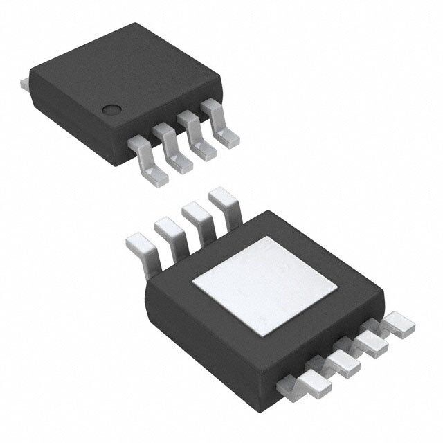
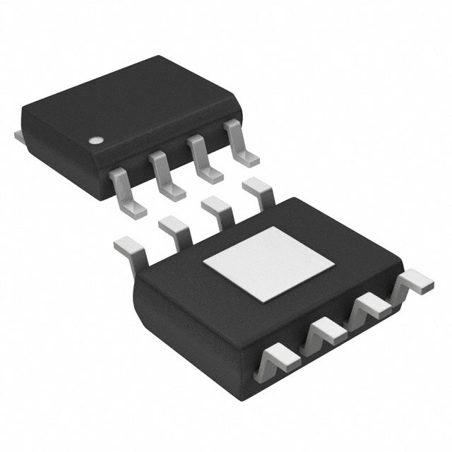
| 供应商器件封装 | 8-SOP-EP |
| 其它名称 | 1028-1214-1 |
| 包装 | 剪切带 (CT) |
| 同步整流器 | 无 |
| 安装类型 | 表面贴装 |
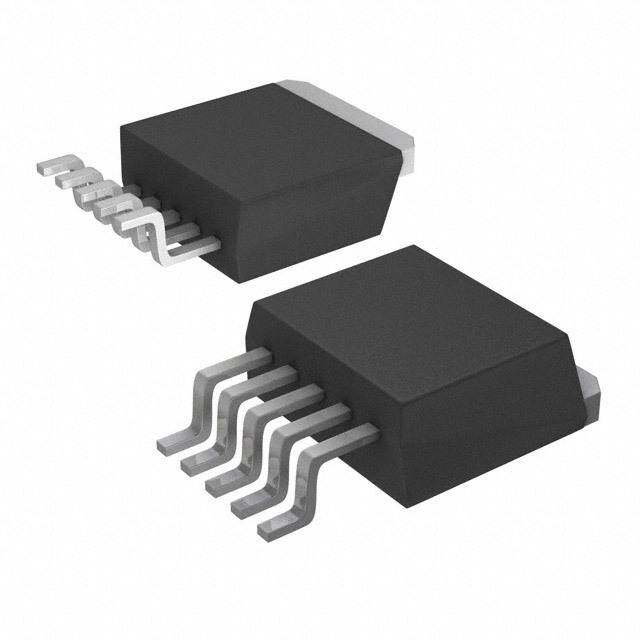
| 封装/外壳 | 8-SOIC(0.154",3.90mm 宽)裸焊盘 |
| 工作温度 | -40°C ~ 85°C |
| 标准包装 | 1 |
| 电压-输入 | 4.5 V ~ 24 V |
| 电压-输出 | 0.808 V ~ 15 V |
| 电流-输出 | 8A |
| 类型 | 降压(降压) |
| 输出数 | 1 |
| 输出类型 | 可调式 |
| 频率-开关 | 600kHz |


- 商务部:美国ITC正式对集成电路等产品启动337调查
- 曝三星4nm工艺存在良率问题 高通将骁龙8 Gen1或转产台积电
- 太阳诱电将投资9.5亿元在常州建新厂生产MLCC 预计2023年完工
- 英特尔发布欧洲新工厂建设计划 深化IDM 2.0 战略
- 台积电先进制程称霸业界 有大客户加持明年业绩稳了
- 达到5530亿美元!SIA预计今年全球半导体销售额将创下新高
- 英特尔拟将自动驾驶子公司Mobileye上市 估值或超500亿美元
- 三星加码芯片和SET,合并消费电子和移动部门,撤换高东真等 CEO
- 三星电子宣布重大人事变动 还合并消费电子和移动部门
- 海关总署:前11个月进口集成电路产品价值2.52万亿元 增长14.8%


PDF Datasheet 数据手册内容提取
® RT7258 8A, 24V, 600kHz Step-Down Converter with Synchronous Gate Driver General Description Features The RT7258 is a synchronous step-down DC/DC converter 4.5V to 24V Input Voltage Range with an integrated high side internal power MOSFET and 8A Output Current a gate driver for a low side external power MOSFET. It 45mΩΩΩΩΩ Internal High Side N-MOSFET can deliver up to 8A output current from a 4.5V to 24V Current Mode Control input supply. The RT7258's current mode architecture 600kHz Switching Frequency allows the transient response to be optimized over a wider Adjustable Output from 0.808V to 15V input voltage and load range. Cycle-by-cycle current limit Up to 95% Efficiency provides protection against shorted outputs and soft-start Internal Compensation eliminates input current surge during start-up. The RT7258 Stable with Ceramic Capacitors is synchronizable to an external clock with frequency Synchronous External Clock : 300kHz to 1.5MHz ranging from 300kHz to 1.5MHz. Cycle-by-Cycle Current Limit Input Under Voltage Lockout The RT7258 is available in WDFN-14L 4x3 and SOP-8 Output Under Voltage Protection (Exposed Pad) packages. Power Good Indicator Thermal Shutdown Protection Applications RoHS Compliant and Halogen Free Point of Load Regulator in Distributed Power System Digital Set top Boxes Personal Digital Recorders Broadband Communications Flat Panel TVs and Monitors Simplified Application Circuit RT7258 VIN VIN BOOT CIN CBOOT L SW VOUT VCC BG Q1 CVCC R1 COUT Power Good PGOOD FB R2 Chip Enable EN/SYNC GND Copyright © 2013 Richtek Technology Corporation. All rights reserved. is a registered trademark of Richtek Technology Corporation. DS7258-01 November 2013 www.richtek.com 1
RT7258 Ordering Information Marking Information RT7258 RT7258GQW Package Type 13= : Product Code QW : WDFN-14L 4x3 (W-Type) 13=YM YMDNN : Date Code SP : SOP-8 (Exposed Pad-Option 2) DNN Lead Plating System G : Green (Halogen Free and Pb Free) Note : RT7258GSP Richtek products are : RT7258GSP : Product Number RoHS compliant and compatible with the current require- RT7258 YMDNN : Date Code GSPYMDNN ments of IPC/JEDEC J-STD-020. Suitable for use in SnPb or Pb-free soldering processes. Pin Configurations (TOP VIEW) FB 1 14 GND PGOOD 2 13 BG SW 8 VIN EN/SYNC 3 12 VCC BOOT 2 7 EN/SYNC VIN 4 GND 11 BOOT GND VIN 5 10 SW VCC 3 6 FB 9 VIN 6 9 SW BG 4 5 GND NC 7 15 8 SW WDFN-14L 4x3 SOP-8 (Exposed Pad) Copyright © 2013 Richtek Technology Corporation. All rights reserved. is a registered trademark of Richtek Technology Corporation. www.richtek.com DS7258-01 November 2013 2
RT7258 Functional Pin Description Pin No. Pin Name Pin Function SOP-8 WDFN-14L 4x3 (Exposed Pad) Feedback Input. This pin is connected to the converter output. It is used to set the output of the converter to regulate to the 1 6 FB desired value via an external resistive divider. The feedback reference voltage is 0.808V typically. Power Good Indicator with Open Drain. (for RT7258GQW only) A 100k pull-high resistor is needed. The output of this pin is 2 -- PGOOD pulled to low when the FB is lower than 0.75V; otherwise it is high impedance. Enable or External Frequency Synchronization Input. A logic-high (2V < EN < 5.5V) enables the converter; a logic-low 3 7 EN/SYNC forces the IC into shutdown mode reducing the supply current to less than 3A. For external frequency synchronization operation, the available frequency range is from 300kHz to 1.5MHz. Power Input. The available input voltage range is from 4.5V to 4, 5, 6 8 VIN 24V. A 22F or larger input capacitor is needed to reduce voltage spikes at the input. 7 -- NC No Internal Connection. Switching Node. Output of the internal high side MOSFET. 8, 9, 10 1 SW Connect this pin to external low side N-MOSFET, inductor and bootstrap capacitor. Bootstrap for High side Gate Driver. Connect a 1F ceramic 11 2 BOOT capacitor between the BOOT pin and SW pin. BG Driver Bias Supply. Decouple with a 1F X5R/X7R ceramic 12 3 VCC capacitor between the VCC pin and GND. Gate Driver Output. Connect this pin to the gate of the external 13 4 BG low side N-MOSFET. 14, 5, Ground. The exposed pad must be soldered to a large PCB and GND 15 (Exposed Pad) 9 (Exposed Pad) connected to GND for maximum thermal dissipation. Copyright © 2013 Richtek Technology Corporation. All rights reserved. is a registered trademark of Richtek Technology Corporation. DS7258-01 November 2013 www.richtek.com 3
RT7258 Function Block Diagram VIN VCC VCC Internal Regulator OSC Enable Slope Current Sense Comparator Compensator Amplifier + 1.7V + RSENSE - EN/SYNC - Foldback 5k 3V Control VCC OTP BOOT UV Comparator Switch 45m VCC 0.4V + Controller SW - Current Signal + 0.808V + COMP VSS -+EA - CCoumrrepnatr ator DBrivGe r BG 54pF 300k FB PGOOD 1pF Comparator PGOOD 0.75V + - GND Operation The RT7258 is a synchronous high voltage Buck Converter side MOSFET. The output under voltage protection is that can support the input voltage range from 4.5V to 24V designed to operate in Hiccup mode. and the output current can be up to 8A. The RT7258 uses Oscillator (OSC) : The internal oscillator runs at nominal a constant frequency, current mode architecture. In normal frequency 600kHz and can be synchronized by an external operation, the high side N-MOSFET is turned on when clock in the range between 300kHz and 1.5MHz from EN/ the Switch Controller is set by the oscillator (OSC) and is SYNC pin. turned off when the current comparator resets the Switch PGOOD Comparator : This function is available for Controller. While the N-MOSFET is turned off, the external RT7258GQW only. When the feedback voltage (V ) is FB low side N-MOSFET is turned on by BG Driver with 5V higher than threshold voltage 0.75V, the PGOOD open driving voltage from Internal Regulator (V ) until next CC drain output will be high impedance. cycle begins. Enable Comparator : Internal 5kΩ resistor and Zener diode High side MOSFET peak current is measured by internal are used to clamp the input signal to 3V. A 1.7V reference R . The Current Signal is where Slope Compensator SENSE voltage is for EN logic-high threshold voltage. The EN pin works together with sensing voltage of R . The error SENSE can be connected to VIN through a 100kΩ resistor for amplifier EA adjusts COMP voltage by comparing the automatic startup. feedback signal (V ) from the output voltage with the FB internal 0.808V reference. When the load current Foldback Control : When VFB is lower than 0.7V, the increases, it causes a drop in the feedback voltage relative oscillation frequency will be proportional to the feedback to the reference, the COMP voltage then rises to allow voltage. higher inductor current to match the load current. Soft-Start (SS) : An internal current source charges an UV Comparator : If the feedback voltage (VFB) is lower internal capacitor to build the soft-start ramp voltage (VSS). than threshold voltage 0.4V, the UV Comparator's output The VFB voltage will track the internal ramp voltage during will go high and the Switch Controller will turn off the high soft-start interval. The typical soft-start time is 2ms. Copyright © 2013 Richtek Technology Corporation. All rights reserved. is a registered trademark of Richtek Technology Corporation. www.richtek.com DS7258-01 November 2013 4
RT7258 Absolute Maximum Ratings (Note 1) Supply Input Voltage, V ------------------------------------------------------------------------------------------ –0.3V to 26V IN Switching Voltage, SW -------------------------------------------------------------------------------------------- –0.3V to (V + 0.3V) IN SW (AC) < 20ns----------------------------------------------------------------------------------------------------- –5V to 30V BOOT to SW --------------------------------------------------------------------------------------------------------- –0.3V to 6V All Other Voltage ---------------------------------------------------------------------------------------------------- −0.3V to 6V Power Dissipation, P @ T = 25°C D A WDFN-14L 4x3------------------------------------------------------------------------------------------------------- 1.667W SOP-8 (Exposed Pad) --------------------------------------------------------------------------------------------- 1.333W Package Thermal Resistance (Note 2) WDFN-14L 4x3, θ ------------------------------------------------------------------------------------------------- 60°C/W JA WDFN-14L 4x3, θ ------------------------------------------------------------------------------------------------- 7.5°C/W JC SOP-8 (Exposed Pad), θ ---------------------------------------------------------------------------------------- 75°C/W JA SOP-8 (Exposed Pad), θ --------------------------------------------------------------------------------------- 15°C/W JC Lead Temperature (Soldering, 10 sec.)------------------------------------------------------------------------- 260°C Junction Temperature----------------------------------------------------------------------------------------------- 150°C Storage Temperature Range -------------------------------------------------------------------------------------- –65°C to 150°C ESD Susceptibility (Note 3) HBM (Human Body Mode) ---------------------------------------------------------------------------------------- 2kV MM (Machine Mode)------------------------------------------------------------------------------------------------ 200V Recommended Operating Conditions (Note 4) Supply Input Voltage, V ------------------------------------------------------------------------------------------ 4.5V to 24V IN Junction Temperature Range-------------------------------------------------------------------------------------- −40°C to 125°C Ambient Temperature Range-------------------------------------------------------------------------------------- −40°C to 85°C Electrical Characteristics (VIN = 12V, TA= 25°C, unless otherwise specified) Parameter Symbol Test Conditions Min Typ Max Unit Shutdown Supply Current VEN = 0V -- 1 -- A Supply Current VEN = 3V, VFB = 1V -- 0.9 -- mA Reference Voltage VREF 4.5V VIN 24V 0.796 0.808 0.82 V Feedback Current IFB VFB = 0.8V -- 10 -- nA High Side Switch On Resistance RDS(ON) -- 45 -- m High Side Switch Current Limit BOOT SW = 4.8V -- 13 -- A Oscillation Frequency fOSC1 -- 600 -- kHz Short Circuit Oscillation Frequency fOSC2 VFB = 0V -- 190 -- kHz Maximum Duty Cycle DMAX VFB = 0.6V -- 90 -- % Minimum On-Time tON VFB = 1V -- 100 -- ns Input Under Voltage Lockout Threshold VUVLO 4 4.2 4.4 V Input Under Voltage Lockout Threshold VUVLO -- 400 -- mV Hysteresis Copyright © 2013 Richtek Technology Corporation. All rights reserved. is a registered trademark of Richtek Technology Corporation. DS7258-01 November 2013 www.richtek.com 5
RT7258 Parameter Symbol Test Conditions Min Typ Max Unit EN Threshold Logic-High VIH 2 -- 5.5 V Voltage Logic-Low VIL -- -- 0.4 Sync Frequency Range fSync 0.3 -- 1.5 MHz EN Turn-Off Delay tOFF -- 10 -- s EN Pull Low Current VEN = 2V -- 1 -- A Thermal Shutdown TSD -- 150 -- C Thermal Shutdown Hysteresis T -- 20 -- C SD Power Good Threshold Rising -- 0.75 -- V Power Good Threshold Hysteresis -- 40 -- mV Power Good Pin Level PGOOD Sink 10mA -- -- 0.125 V BG Driver Bias Supply Voltage VCC 4.5 5 -- V Gate Driver Sink Impedance RSink -- 0.9 -- Gate Driver Source Impedance RSource -- 3.3 -- Note 1. Stresses beyond those listed “Absolute Maximum Ratings” may cause permanent damage to the device. These are stress ratings only, and functional operation of the device at these or any other conditions beyond those indicated in the operational sections of the specifications is not implied. Exposure to absolute maximum rating conditions may affect device reliability. Note 2. θJA is measured at TA= 25°C on a high effective thermal conductivity four-layer test board per JEDEC 51-7. θJC is measured at the exposed pad of the package. Note 3. Devices are ESD sensitive. Handling precaution is recommended. Note 4. The device is not guaranteed to function outside its operating conditions. Copyright © 2013 Richtek Technology Corporation. All rights reserved. is a registered trademark of Richtek Technology Corporation. www.richtek.com DS7258-01 November 2013 6
RT7258 Typical Application Circuit For WDFN-14L 4x3 Package RT7258 VIN 4, 5, 6 VIN BOOT 11 4.5V to 24V CIN CBOOT 22µF 1µF L 2.2µH SW 8, 9, 10 VOUT 3.3V 12 VCC 13 BG Q1 CVCC R1 1µF 62k R3 1 COUT 100k FB 22µF x 4 2 R2 Power Good PGOOD 20k Chip Enable 3 GND 14, 15 (Exposed Pad) EN/SYNC For SOP-8 (Exposed Pad) Package RT7258 VIN 8 VIN BOOT 2 4.5V to 24V CIN CBOOT 22µF 1µF L 2.2µH SW 1 VOUT 3.3V 3 VCC 4 BG Q1 CVCC R1 1µF 62k 6 COUT FB 22µF x 4 Chip Enable 7 5, 9 (Exposed Pad) R2 EN/SYNC GND 20k Table 1. Recommended Component Selection VOUT (V) R1 (k) R2 (k) L (H) COUT (F) 1.2 62 127 1.5 22F x 4 1.8 70 57 1.5 22F x 4 2.5 69 33 2.2 22F x 4 3.3 62 20 2.2 22F x 4 5 93 18 2.8 22F x 4 8 120 13.5 3.6 22F x 4 Copyright © 2013 Richtek Technology Corporation. All rights reserved. is a registered trademark of Richtek Technology Corporation. DS7258-01 November 2013 www.richtek.com 7
RT7258 Typical Operating Characteristics Efficiency vs. Load Current Output Voltage vs. Input Voltage 100 3.33 90 3.32 80 VIN = 10V ) y (%) 6700 VVIINN == 1224VV age (V 3.31 nc 50 olt 3.30 e V Effici 3400 utput 3.29 O 20 3.28 10 VOUT = 3.3V VIN = 4.5V to 24V, VOUT = 3.3V, IOUT = 0A 0 3.27 0 2 4 6 8 4 6 8 10 12 14 16 18 20 22 24 Load Current (A) Input Voltage (V) Output Voltage vs. Temperature Output Voltage vs. Load Current 3.40 3.35 3.38 3.34 3.36 3.33 V) 3.34 V) 3.32 e ( e ( g 3.32 g 3.31 a a olt 3.30 olt 3.30 V V ut 3.28 ut 3.29 VIN = 10V utp 3.26 utp 3.28 VIN = 12V O O VIN = 24V 3.24 3.27 3.22 3.26 VIN = 12V, VOUT = 3.3V, IOUT = 0A VOUT = 3.3V 3.20 3.25 -50 -25 0 25 50 75 100 125 0 1 2 3 4 5 6 7 8 Temperature (°C) Load Current (A) Switching Frequency vs. Input Voltage Switching Frequency vs. Temperature 650 650 z) 1 640 z) 1 640 H 630 H 630 k k y ( 620 y ( 620 c c n n e 610 e 610 u u eq 600 eq 600 Fr Fr g 590 ng 590 hin 580 chi 580 witc 570 wit 570 S S 560 560 VOUT = 3.3V, IOUT = 0A VIN = 12V, VOUT = 3.3V, IOUT = 0A 550 550 4 6 8 10 12 14 16 18 20 22 24 -50 -25 0 25 50 75 100 125 Input Voltage (V) Temperature (°C) Copyright © 2013 Richtek Technology Corporation. All rights reserved. is a registered trademark of Richtek Technology Corporation. www.richtek.com DS7258-01 November 2013 8
RT7258 Current Limit vs. Temperature Load Transient Response 18 17 VOUT ) 16 (100mV/Div) A nt ( 15 e rr u 14 C put 13 Out 12 (5IAO/UDTiv) 11 VIN = 12V, VOUT = 3.3V VIN = 12V, VOUT = 3.3V, IOUT = 0A to 8A 10 -50 -25 0 25 50 75 100 125 Time (500μs/Div) Temperature (°C) Load Transient Response Output Ripple Voltage VOUT (5mV/Div) VOUT (100mV/Div) VSW (10V/Div) IOUT (5A/Div) IL (2A/Div) VIN = 12V, VOUT = 3.3V, IOUT = 4A to 8A VIN = 12V, VOUT = 3.3V, IOUT = 4A Time (500μs/Div) Time (1μs/Div) Output Ripple Voltage Power On from VIN VOUT (5mV/Div) VIN (5V/Div) VSW (10V/Div) VOUT (2V/Div) IL IL (5A/Div) (10A/Div) VIN = 12V, VOUT = 3.3V, IOUT = 8A VIN = 12V, VOUT = 3.3V, IOUT = 8A Time (1μs/Div) Time (5ms/Div) Copyright © 2013 Richtek Technology Corporation. All rights reserved. is a registered trademark of Richtek Technology Corporation. DS7258-01 November 2013 www.richtek.com 9
RT7258 Power Off from VIN Power On from EN VEN (5V/Div) VIN (5V/Div) VOUT (2V/Div) VOUT (2V/Div) IL (10A/Div) IL (10A/Div) VIN = 12V, VOUT = 3.3V, IOUT = 8A VIN = 12V, VOUT = 3.3V, IOUT = 8A Time (5ms/Div) Time (2.5ms/Div) Power Off from EN External SYNC VEN Clock (5V/Div) (5V/Div) VOUT VLX (2V/Div) (10V/Div) IL IL (5A/Div) (10A/Div) VOUT (2V/Div) VIN = 12V, VOUT = 3.3V, IOUT = 8A VIN = 12V, VOUT = 3.3V, IOUT = 8A, Clock = 500kHz Time (2.5ms/Div) Time (1μs/Div) Copyright © 2013 Richtek Technology Corporation. All rights reserved. is a registered trademark of Richtek Technology Corporation. www.richtek.com DS7258-01 November 2013 10
RT7258 Application Information can also be externally pulled high by adding a R resistor Output Voltage Setting EN and C capacitor from the VIN pin (see Figure 3). EN The resistive divider allows the FB pin to sense the output EN voltage as shown in Figure 1. REN VIN EN VOUT RT7258 CEN R1 GND FB RT7258 R2 Figure 3. Enable Timing Control GND An external MOSFET can be added to implement digital Figure 1. Output Voltage Setting control on the EN pin, as shown in Figure 4. In this case, a 100kΩ pull-up resistor, R , is connected between V EN IN The output voltage is set by an external resistive voltage pin and the EN pin. MOSFET Q2 will be under logic control divider according to the following equation : to pull down the EN pin. R1 VOUT = VREF1R2 REN 100k Where VREF is the feedback voltage (0.808V typ.). VIN EN EN Q2 RT7258 External Bootstrap Diode Connect a 1μF low ESR ceramic capacitor between the GND BOOT pin and SW pin. This capacitor provides the gate Figure 4. Digital Enable Control Circuit driver voltage for the high side MOSFET. The chip starts to operate when V rises to 4.2V (UVLO IN It is recommended to add an external bootstrap diode threshold). During the V rising period, if an 8V output IN between an external 5V and BOOT pin for efficiency voltage is set, V is lower than the V target value and IN OUT improvement when input voltage is lower than 5.5V or duty it may cause the chip to shut down. To prevent this ratio is higher than 65% .The bootstrap diode can be a situation, a resistive voltage divider can be placed between low cost one such as IN4148 or BAT54. The external 5V the input voltage and ground and connected to the EN pin can be a 5V fixed input from system or a 5V output of the to adjust enable threshold, as shown in Figure 5. For RT7258. Note that the external boot voltage must be lower example, the setting V is 8V and V is from 0V to OUT IN than 5.5V. 12V, when V is higher than 10V, the chip is triggered to 5V IN enable the converter. Assume R = 50kΩ. Then, EN1 (REN1 x VEN_T) REN2 = BOOT (VIN_SVEN_T) RT7258 1µF where V is the enable comparator's logic-high reference EN_T SW threshold voltage (1.7V) and V is the target turn on IN_S input voltage (10V in this example). According to the Figure 2. External Bootstrap Diode equation, the suggested resistor R is 10.2kΩ. EN2 Chip Enable Operation REN1 VIN EN The EN pin is the chip enable input. Pulling the EN pin low (<0.4V) will shutdown the device. During shutdown REN2 RT7258 mode, the RT7258 quiescent current drops to lower than GND 3μA. Driving the EN pin high (2V < EN < 5.5V) will turn on the device again. For external timing control, the EN pin Figure 5. Resistor Divider for Lockout Threshold Setting Copyright © 2013 Richtek Technology Corporation. All rights reserved. is a registered trademark of Richtek Technology Corporation. DS7258-01 November 2013 www.richtek.com 11
RT7258 Soft-Start Over Temperature Protection The RT7258 provides soft-start function. The soft-start The RT7258 features an Over Temperature Protection function is used to prevent large inrush current while (OTP) circuitry to prevent from overheating due to converter is being powered-up. An internal current source excessive power dissipation. The OTP will shut down charges an internal capacitor to build a soft-start ramp switching operation when junction temperature exceeds voltage. The V voltage will track the internal ramp voltage 150°C. Once the junction temperature cools down by FB during soft-start interval. The typical softstart time is 2ms. approximately 20°C, the converter will resume operation. To maintain continuous operation, the maximum junction Operating Frequency and Synchronization temperature should be lower than 125°C. The internal oscillator runs at 600kHz (typ.) when the EN/ Under Voltage Protection SYNC pin is at logic-high level (>2V). If the EN pin is pulled to low-level for 10μs above, the IC will shut down. For the RT7258, it provides Hiccup Mode Under Voltage Protection (UVP). When the V voltage drops below 0.4V, The RT7258 can be synchronized with an external clock FB the UVP function will be triggered to shut down switching ranging from 300kHz to 1.5MHz applied to the EN/SYNC operation. If the UV condition remains for a period, the pin. The external clock duty cycle must be from 10% to RT7258 will retry every 2ms. When the UV condition is 90%. removed, the converter will resume operation. The UVP 3.5ms (Start-up period) 10µs is disabled during soft-start period. Hiccup Mode EN/SYNC VFB VOUT CLK (1V/Div) Foldback External CLK 600kHz IL (10A/Div) Figure 6. Startup Sequence Using External Sync Clock VIN = 12V, IOUT = Short Figure 6 shows the synchronization operation in startup Time (2.5ms/Div) period. When the EN/SYNC is triggered by an external clock, the RT7258 enters soft-start phase and the output Figure 7. Hiccup Mode Under Voltage Protection voltage starts to rise. When V is lower than 0.7V, the FB oscillation frequency will be proportional to the feedback Duty Cycle Limitation voltage. With higher VFB, the switching frequency is The RT7258 has a maximum duty cycle 90%. The relatively higher. After startup period about 3.5ms, the IC minimum input voltage is determined by the maximum operates with the same frequency as the external clock. duty cycle and its minimum operating voltage 4.5V. The voltage drops of high side MOSFET and low side MOSFET also must be considered for the minimum input voltage. The minimum duty cycle can be calculated by the following equation : Duty Cycle(min) = f x t (min) SW ON Copyright © 2013 Richtek Technology Corporation. All rights reserved. is a registered trademark of Richtek Technology Corporation. www.richtek.com DS7258-01 November 2013 12
RT7258 where fsw is the switching frequency, t (min) is the For the ripple current selection, the value of ΔI = 0.24(I ) ON L MAX minimum switch on time (100ns). This equation shows will be a reasonable starting point. The largest ripple that the minimum duty cycle increases when the switching current occurs at the highest V . To guarantee that the IN frequency is increased. Therefore, slower switching ripple current stays below the specified maximum, the frequency is necessary to achieve high V /V ratio inductor value should be chosen according to the following IN OUT application. equation : L = VOUT 1 VOUT External N-MOSFET Selection fIL(MAX) VIN(MAX) The RT7258 is designed to operate using an external low The inductor's current rating (cause a 40°C temperature side N-MOSFET. Important parameters for the power rising from 25°C ambient) should be greater than the MOSFETs are the breakdown voltage (BV ), threshold DSS maximum load current and its saturation current should voltage (V ), on-resistance (R ), total gate charge GS_TH DS(ON) be greater than the short circuit peak current limit. Please (Qg) and maximum current (I ). The gate driver voltage D(MAX) see Table 3 for the inductor selection reference. is from internal regulator (5V, V ). Therefore logic level CC N-MOSFET must be used in the RT7258 application. The Table 3. Suggested Inductors for Typical total gate charge (Qg) must be less than 50nC, lower Qg Application Circuit characteristics results in lower power losses. Drain-source Component Dimensions Series Supplier (mm) on-resistance (R ) should be as small as possible, DS(ON) 10 x 10 x 4 less than 30mΩ is desirable. Lower RDS(ON) results in Zenithtek ZPWM 6 x 6 x 3 higher efficiency. WE 74477 10 x 10 x 4 Table 2. External N-MOSFET Selection TAIYOYUDEN NR8040 8 x 10 x 4 Part No. Manufacture Si7114 Vishay C and C Selection A04474 ALPHA & OMEGA IN OUT The input capacitance, C is needed to filter the FDS6670AS Fairchild IN, trapezoidal current at the source of the high side MOSFET. IRF7821 International Rectifier To prevent large ripple current, a low ESR input capacitor sized for the maximum RMS current should be used. The Inductor Selection approximate RMS current equation is given : The inductor value and operating frequency determine the ripple current according to a specific input and output IRMS = IOUT(MAX) VOUT VIN 1 VIN VOUT voltage. The ripple current ΔI increases with higher V L IN This formula has a maximum at V = 2V , where and decreases with higher inductance. IN OUT I = I / 2. This simple worst case condition is IL =VfOULT1VVOIUNT cRoMmS monOlUyT used for design because even significant deviations do not offer much relief. Having a lower ripple current reduces not only the ESR Choose a capacitor rated at a higher temperature than losses in the output capacitors but also the output voltage required. Several capacitors may also be paralleled to ripple. High frequency with small ripple current can reduce meet size or height requirements in the design. voltage. For the highest efficiency operation, however, it requires a large inductor to achieve this goal. Copyright © 2013 Richtek Technology Corporation. All rights reserved. is a registered trademark of Richtek Technology Corporation. DS7258-01 November 2013 www.richtek.com 13
RT7258 Table 4. Suggested Capacitors for C and C IN OUT Location Component Supplier Part No. Capacitance (F) Case Size C MURATA GRM31CR61E106K 10 1206 IN CIN TDK C3225X5R1E106K 10 1206 CIN TAIYO YUDEN TMK316BJ106ML 10 1206 C MURATA GRM31CR60J476M 47 1206 OUT COUT TDK C3225X5R0J476M 47 1210 C MURATA GRM32ER71C226M 22 1210 OUT COUT TDK C3225X5R1C22M 22 1210 For the input capacitor, two 10μF low ESR ceramic Checking Transient Response capacitors are recommended. For the recommended The regulator loop response can be checked by looking capacitor, please refer to Table 4 for more details. at the load transient response. Switching regulators take The selection of C is determined by the required ESR several cycles to respond to a step load change. When a OUT to minimize voltage ripple. step load occurs, VOUTimmediately shifts by an amount equal to ΔI x ESR also begins to charge or discharge LOAD Moreover, the amount of bulk capacitance is also a key C generating a feedback error signal for the regulator OUT for C selection to ensure that the control loop is stable. OUT to return V to its steady-state value. During this OUT Loop stability can be checked by viewing the load transient recovery time, V can be monitored for overshoot or OUT response as described in a later section. ringing that would indicate a stability problem. The output ripple, ΔV , is determined by : OUT 1 Thermal Considerations VOUT ILESR8fCOUT For continuous operation, do not exceed absolute maximum junction temperature. The maximum power The output ripple will be the highest at the maximum input dissipation depends on the thermal resistance of the IC voltage since ΔI increases with input voltage. Multiple L package, PCB layout, rate of surrounding airflow, and capacitors placed in parallel may be needed to meet the difference between junction and ambient temperature. The ESR and RMS current handling requirement. maximum power dissipation can be calculated by the Higher values, lower cost ceramic capacitors are now following formula : becoming available in smaller case sizes. Their high ripple P = (T − T ) / θ D(MAX) J(MAX) A JA current, high voltage rating and low ESR make them ideal where T is the maximum junction temperature, T is for switching regulator applications. When a ceramic J(MAX) A the ambient temperature, and θ is the junction to ambient capacitor is used at the input and the power is supplied JA thermal resistance. by a wall adapter through long wires, a load step at the output can induce ringing at the input, V . This ringing For recommended operating condition specifications of IN can couple to the output and be mistaken. A sudden inrush the RT7258, the maximum junction temperature is 125°C. of current through the long wires can potentially cause a The junction to ambient thermal resistance, θ , is layout JA voltage spike at V large enough to damage the part. dependent. For SOP-8 (Exposed Pad) package, the IN thermal resistance, θ , is 75°C/W on a standard JEDEC JA 51-7 four-layer thermal test board. Copyright © 2013 Richtek Technology Corporation. All rights reserved. is a registered trademark of Richtek Technology Corporation. www.richtek.com DS7258-01 November 2013 14
RT7258 For WDFN-14L 4x3 package, the thermal resistance, θ , Layout Consideration JA is 60°C/W on a standard JEDEC 51-7 four-layer thermal Follow the PCB layout guidelines for optimal performance test board. The maximum power dissipation at TA = 25°C of the RT7258. can be calculated by the following formulas : Keep the traces of the main current paths as short and PD(MAX) = (125°C − 25°C) / (75°C/W) = 1.333W for wide as possible. SOP-8 (Exposed Pad) package Put the input capacitor as close as possible to the device PD(MAX) = (125°C − 25°C) / (60°C/W) = 1.667W for pins (VIN and GND). WDFN-14L 4x3 package SW node is with high frequency voltage swing and The maximum power dissipation depends on the operating should be kept at small area. Keep analog components ambient temperature for fixed TJ(MAX) and thermal away from the SW node to prevent stray capacitive noise resistance, θJA. For the RT7258 package, the derating pick-up. curves in Figure 8 allow the designer to see the effect of Connect feedback network behind the output capacitors. rising ambient temperature on the maximum power Keep the loop area small. Place the feedback dissipation. components near the RT7258. 1.8 ) 1 Four-Layer PCB Connect all analog grounds to a common node and then W 1.6 connect the common node to the power ground behind on ( 1.4 the output capacitors. ati sip 1.2 WDFN-14L 4x3 An example of PCB layout guide is shown in Figure 9 s Di 1.0 and Figure 10 for reference. r e 0.8 w o SOP-8 (Exposed Pad) P 0.6 m u 0.4 m axi 0.2 M 0.0 0 25 50 75 100 125 Ambient Temperature (°C) Figure 8. Derating Curves for RT7258 Package Copyright © 2013 Richtek Technology Corporation. All rights reserved. is a registered trademark of Richtek Technology Corporation. DS7258-01 November 2013 www.richtek.com 15
RT7258 SW should be connected to inductor by Input capacitor must be placed wide and short trace. Keep sensitive as close to the IC as possible. components away from this trace. GND VIN The EN/SYNC must be kept COUT Q1 BG CIN away from noise. The trace should be short and shielded L with a ground trace. VOUT CBOOT SW 8 VIN BOOT 2 7 EN/SYNCGND CVCC capacitor must GND be placed as close to VCC 3 6 FB 9 R1 VOUT the IC as possible. CVCC BG 4 5 GND R2 The feedback components must be connected as close GND to the device as possible. Figure 9. PCB Layout Guide for SOP-8 (Exposed Pad) The feedback components GND must be connected as close R2 to the device as possible. CVCC capacitor must be placed as close to VOUT R1 the IC as possible. FB 1 14 GND R3 VCC PGOOD 2 13 BG CVCC GNDEN/SYNC 3 12 VCC Tawhea yE fNro/SmY nNoCis me. uTsht eb etr akceep t VIN VVIINN 45 GND 1110 SBWOOT CBOOT StoW in sdhuocutoldr bbye wciodnen aencdte d swhitohu ald g broeu snhdo rtrt aacned. shielded CIN VNICN 67 15 98 SSWW L VOUT scohmorpt otrnaecnet.s K aeweapy s fernosmit ive this trace. Q1 BG COUT Input capacitor must be placed as close to the GND IC as possible. Figure 10. PCB Layout Guide for WDFN-14L 4x3 Copyright © 2013 Richtek Technology Corporation. All rights reserved. is a registered trademark of Richtek Technology Corporation. www.richtek.com DS7258-01 November 2013 16
RT7258 Outline Dimension 2 1 2 1 DETAIL A Pin #1 ID and Tie Bar Mark Options Note : The configuration of the Pin #1 identifier is optional, but must be located within the zone indicated. Dimensions In Millimeters Dimensions In Inches Symbol Min Max Min Max A 0.700 0.800 0.028 0.031 A1 0.000 0.050 0.000 0.002 A3 0.175 0.250 0.007 0.010 b 0.180 0.300 0.007 0.012 D 3.900 4.100 0.154 0.161 D2 3.250 3.350 0.128 0.132 E 2.900 3.100 0.114 0.122 E2 1.650 1.750 0.065 0.069 e 0.500 0.020 L 0.350 0.450 0.014 0.018 W-Type 14L DFN 4x3 Package Copyright © 2013 Richtek Technology Corporation. All rights reserved. is a registered trademark of Richtek Technology Corporation. DS7258-01 November 2013 www.richtek.com 17
RT7258 H A M EXPOSED THERMAL PAD Y (Bottom of Package) J X B F C I D Dimensions In Millimeters Dimensions In Inches Symbol Min Max Min Max A 4.801 5.004 0.189 0.197 B 3.810 4.000 0.150 0.157 C 1.346 1.753 0.053 0.069 D 0.330 0.510 0.013 0.020 F 1.194 1.346 0.047 0.053 H 0.170 0.254 0.007 0.010 I 0.000 0.152 0.000 0.006 J 5.791 6.200 0.228 0.244 M 0.406 1.270 0.016 0.050 X 2.000 2.300 0.079 0.091 Option 1 Y 2.000 2.300 0.079 0.091 X 2.100 2.500 0.083 0.098 Option 2 Y 3.000 3.500 0.118 0.138 8-Lead SOP (Exposed Pad) Plastic Package Richtek Technology Corporation 14F, No. 8, Tai Yuen 1st Street, Chupei City Hsinchu, Taiwan, R.O.C. Tel: (8863)5526789 Richtek products are sold by description only. Richtek reserves the right to change the circuitry and/or specifications without notice at any time. Customers should obtain the latest relevant information and data sheets before placing orders and should verify that such information is current and complete. Richtek cannot assume responsibility for use of any circuitry other than circuitry entirely embodied in a Richtek product. Information furnished by Richtek is believed to be accurate and reliable. However, no responsibility is assumed by Richtek or its subsidiaries for its use; nor for any infringements of patents or other rights of third parties which may result from its use. No license is granted by implication or otherwise under any patent or patent rights of Richtek or its subsidiaries. www.richtek.com DS7258-01 November 2013 18