ICGOO在线商城 > 分立半导体产品 > 二极管 - 整流器 - 单 > RS2KA-13-F
 Datasheet下载
- 型号: RS2KA-13-F
- 制造商: Diodes Inc.
- 库位|库存: xxxx|xxxx
- 要求:
| 数量阶梯 | 香港交货 | 国内含税 |
| +xxxx | $xxxx | ¥xxxx |
查看当月历史价格
查看今年历史价格
RS2KA-13-F产品简介:
ICGOO电子元器件商城为您提供RS2KA-13-F由Diodes Inc.设计生产,在icgoo商城现货销售,并且可以通过原厂、代理商等渠道进行代购。 RS2KA-13-F价格参考。Diodes Inc.RS2KA-13-F封装/规格:二极管 - 整流器 - 单, 标准 表面贴装 二极管 800V 1.5A SMA。您可以下载RS2KA-13-F参考资料、Datasheet数据手册功能说明书,资料中有RS2KA-13-F 详细功能的应用电路图电压和使用方法及教程。
Diodes Incorporated的RS2KA-13-F是一款肖特基整流器二极管,属于二极管 - 整流器 - 单类别。其应用场景广泛,适用于多种电力电子设备和系统中。以下是该型号的主要应用场景:

1. 电源适配器与充电器:
   RS2KA-13-F因其低正向电压降(Vf)特性,能够高效地将交流电转换为直流电,适用于各种电源适配器和充电器电路中的整流功能,减少功率损耗并提高效率。

2. 开关电源(SMPS):
   在开关模式电源中,该二极管可用于输出整流阶段,帮助实现高效的直流电压输出。其快速恢复特性和低反向漏电流使其非常适合高频开关应用。

3. 太阳能光伏系统:
   在光伏电池板的旁路保护电路中,RS2KA-13-F可以防止电流反向流动,从而避免因阴影或故障导致的电池板损坏,并确保系统的稳定运行。

4. 电机驱动与控制:
   用于电机驱动电路中的整流或续流功能,可有效处理电机运行时产生的反电动势,保护电路免受损害。

5. 汽车电子:
   在汽车电子系统中,例如车载充电器、LED照明驱动器和传感器接口等,该二极管能提供可靠且高效的整流性能,适应严苛的工作环境。

6. 消费类电子产品:
   包括电视、音响设备和其他家用电器的电源部分,RS2KA-13-F可以作为整流元件,支持设备的正常运行。

7. 工业自动化:
   在工业控制领域,如PLC模块、传感器信号调理电路以及变频器中,该二极管可用于整流或其他相关功能,满足高可靠性和耐用性的要求。

总结来说,RS2KA-13-F凭借其出色的电气特性和稳定性,特别适合需要高效整流、低功耗和快速响应的应用场合,是许多现代电子设备的理想选择。
| 参数 | 数值 |
| 产品目录 | |
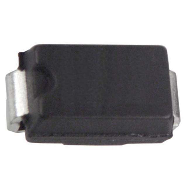
| 描述 | DIODE FAST REC 800V 1.5A SMA |
| 产品分类 | 单二极管/整流器 |
| 品牌 | Diodes Incorporated |
| 数据手册 | |
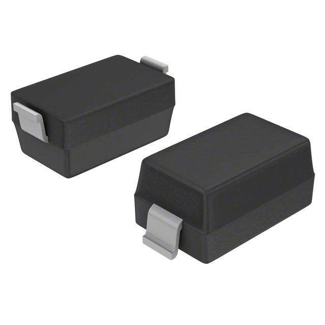
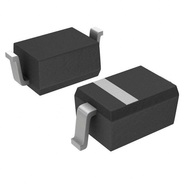
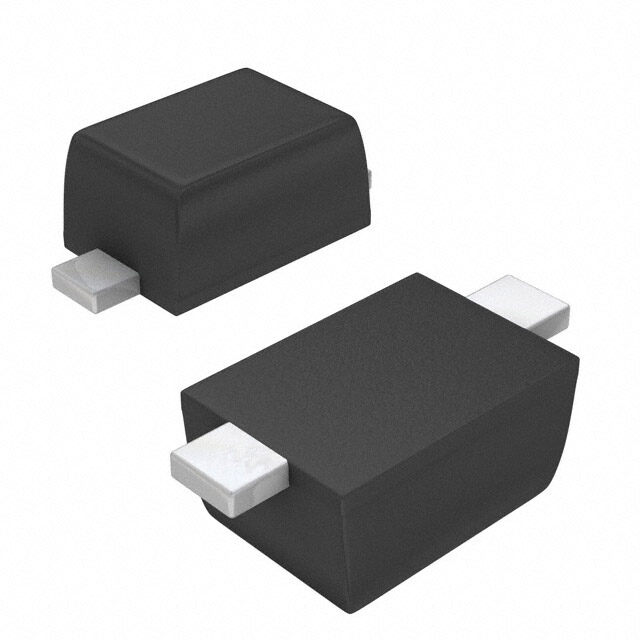
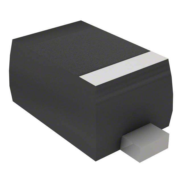
| 产品图片 |
|
| 产品型号 | RS2KA-13-F |
| rohs | 不受无铅要求限制 / 符合限制有害物质指令(RoHS)规范要求 |
| RoHS指令信息 | http://diodes.com/download/4349 |
| 产品系列 | - |
| 不同If时的电压-正向(Vf) | 1.3V @ 1.5A |
| 不同 Vr、F时的电容 | 30pF @ 4V,1MHz |
| 不同 Vr时的电流-反向漏电流 | 5µA @ 800V |
| 二极管类型 | 标准 |
| 产品目录页面 | |
| 供应商器件封装 | SMA |
| 其它名称 | RS2KA-FDICT |
| 包装 | 剪切带 (CT) |
| 反向恢复时间(trr) | 500ns |
| 安装类型 | 表面贴装 |
| 封装/外壳 | DO-214AC,SMA |
| 工作温度-结 | -65°C ~ 150°C |
| 标准包装 | 1 |
| 热阻 | 20°C/W Jl |
| 电压-DC反向(Vr)(最大值) | 800V |
| 电流-平均整流(Io) | 1.5A |
| 速度 | 快速恢复 =< 500 ns,> 200mA(Io) |


PDF Datasheet 数据手册内容提取
RS2A/A - RS2M/A 1.5A SURFACE MOUNT FAST RECOVERY RECTIFIER Features Mechanical Data • Glass Passivated Die Construction • Case: SMA/SMB • Fast Recovery Time For High Efficiency • Case Material: Molded Plastic. UL Flammability Classification • Surge Overload Rating to 50A Peak Rating 94V-0 • Ideally Suited for Automated Assembly • Moisture Sensitivity: Level 1 per J-STD-020 • Lead Free Finish/RoHS Compliant (Note 1) • Terminals: Lead Free Plating (Matte Tin Finish). Solderable per MIL-STD-202, Method 208 • Green Molding Compound (No Halogen and Antimony) (Note 2) • Polarity: Cathode Band or Cathode Notch • SMA Weight: 0.065 grams (approximate) • SMB Weight: 0.09 grams (approximate) Top View Bottom View Ordering Information (Note 3) Part Number Case Packaging RS2xA-13-F SMA 5000/Tape & Reel RS2x-13-F SMB 3000/Tape & Reel *x = Device type, e.g. RS2DA-13-F (SMA package); RS2J-13-F (SMB package). Notes: 1. EU Directive 2002/95/EC (RoHS). All applicable RoHS exemptions applied, see EU Directive 2002/95/EC Annex Notes. 2. Product manufactured with Data Code 0924 (week 24, 2009) and newer are built with Green Molding Compound. 3. For packaging details, go to our website at http://www.diodes.com. Marking Information RS2x = Product type marking code, ex: RS2G (SMB package) RS2xA = Product type marking code, ex: RS2GA (SMA package) YWW = Manufacturers’ code marking RS2x(A) YWW = Date code marking Y = Last digit of year (ex: 2 for 2002) WW = Week code (01 to 53) RS2A/A - RS2M/A 1 of 4 September 2010 Document number: DS15004 Rev. 11 - 2 www.diodes.com © Diodes Incorporated
RS2A/A - RS2M/A Maximum Ratings @TA = 25°C unless otherwise specified Single phase, half wave, 60Hz, resistive or inductive load. For capacitance load, derate current by 20%. RS2 RS2 RS2 RS2 RS2 RS2 RS2 Characteristic Symbol Unit A/AA B/BA D/DA G/GA J/JA K/KA M/MA Peak Repetitive Reverse Voltage VRRM Working Peak Reverse Voltage VRWM 50 100 200 400 600 800 1000 V DC Blocking Voltage (Note 4) VR RMS Reverse Voltage VR(RMS) 35 70 140 280 420 560 700 V Average Rectified Output Current @ TT = 120°C IO 1.5 A Non-Repetitive Peak Forward Surge Current 8.3ms Single Half Sine-Wave Superimposed on Rated Load IFSM 50 A Thermal Characteristics Characteristic Symbol Value Unit Typical Thermal Resistance, Junction to Terminal (Note 5) RθJT 20 °C/W Operating and Storage Temperature Range TJ, TSTG -65 to +150 °C Electrical Characteristics @TA = 25°C unless otherwise specified RS2 RS2 RS2 RS2 RS2 RS2 RS2 Characteristic Symbol Unit A/AA B/BA D/DA G/GA J/JA K/KA M/MA Forward Voltage @ IF = 1.5A VFM 1.3 V Pate Raka tRede vDeCrs eB lCocukrrinegn tV oltage ( N o t e 4 ) @@ TTAA == 1 2255°°CC IRM 250.00 μA Reverse Recovery Time (Note 6) trr 150 250 500 ns Typical Total Capacitance (Note 7) CT 30 pF Notes: 4. Short duration pulse test used to minimize self-heating effect. 5. Reverse recovery test conditions: I = 0.5A, I = 1.0A, I = 0.25A. See Figure 5. F R rr 6. Thermal Resistance: Junction to terminal, unit mounted on PC board with 5.0 mm2 (0.013 mm thick) copper pads as heat sink. 7. Measured at 1.0MHz and applied reverse voltage of 4.0V DC. 1.5 A) 10 A) NT ( T ( RE N R E U R C UR 1.0 D 1.0 C R D WA FIE OR TI F C S E U R O E 0.5 E 0.1 G N A A R T E N V A A T , O NS TJ = 25°C I IF, I 0 0.01 25 50 75 100 125 150 175 0 0.4 0.8 1.2 1.6 T , TERMINAL TEMPERATURE (°C) V , INSTANTANEOUS FORWARD VOLTAGE (V) T F Fig. 1 Forward Current Derating Curve Fig. 2 Typical Forward Characteristics RS2A/A - RS2M/A 2 of 4 September 2010 Document number: DS15004 Rev. 11 - 2 www.diodes.com © Diodes Incorporated
RS2A/A - RS2M/A T (A) 60 Single Half-Sine-Wave T (µA) 1,000 REN 50 REN TJ = 125°C UR TJ = 150°C UR 100 C C E 40 E G S R R U E S V D 30 E 10 R R A S W U R O O 20 E F N K TA 1.0 TJ = 25°C A N PE 10 TA , M NS IFS 0 I, IR 0.1 1 10 100 0 20 40 60 80 100 120 140 NUMBER OF CYCLES AT 60 Hz PERCENT OF RATED PEAK REVERSE VOLTAGE (%) Fig. 3 Forward Surge Current Derating Curve Fig. 4 Typical Reverse Characteristics Package Outline Dimensions B SMA SMB Dim Min Max Dim Min Max A C A 2.29 2.92 A 3.30 3.94 B 4.00 4.60 B 4.06 4.57 C 1.27 1.63 C 1.96 2.21 D 0.15 0.31 D 0.15 0.31 D E 4.80 5.59 E 5.00 5.59 G 0.05 0.20 G 0.05 0.20 J H 0.76 1.52 H 0.76 1.52 J 2.01 2.30 J 2.00 2.50 H G All Dimensions in mm All Dimensions in mm E RS2A/A - RS2M/A 3 of 4 September 2010 Document number: DS15004 Rev. 11 - 2 www.diodes.com © Diodes Incorporated
RS2A/A - RS2M/A Suggested Pad Layout SMA SMB Dimensions Value (in mm) Dimensions Value (in mm) Z 6.5 Z 6.7 G 1.5 G 1.8 X 1.7 X 2.3 Y 2.5 Y 2.5 C 4.0 C 4.3 IMPORTANT NOTICE DIODES INCORPORATED MAKES NO WARRANTY OF ANY KIND, EXPRESS OR IMPLIED, WITH REGARDS TO THIS DOCUMENT, INCLUDING, BUT NOT LIMITED TO, THE IMPLIED WARRANTIES OF MERCHANTABILITY AND FITNESS FOR A PARTICULAR PURPOSE (AND THEIR EQUIVALENTS UNDER THE LAWS OF ANY JURISDICTION). Diodes Incorporated and its subsidiaries reserve the right to make modifications, enhancements, improvements, corrections or other changes without further notice to this document and any product described herein. Diodes Incorporated does not assume any liability arising out of the application or use of this document or any product described herein; neither does Diodes Incorporated convey any license under its patent or trademark rights, nor the rights of others. Any Customer or user of this document or products described herein in such applications shall assume all risks of such use and will agree to hold Diodes Incorporated and all the companies whose products are represented on Diodes Incorporated website, harmless against all damages. Diodes Incorporated does not warrant or accept any liability whatsoever in respect of any products purchased through unauthorized sales channel. Should Customers purchase or use Diodes Incorporated products for any unintended or unauthorized application, Customers shall indemnify and hold Diodes Incorporated and its representatives harmless against all claims, damages, expenses, and attorney fees arising out of, directly or indirectly, any claim of personal injury or death associated with such unintended or unauthorized application. Products described herein may be covered by one or more United States, international or foreign patents pending. Product names and markings noted herein may also be covered by one or more United States, international or foreign trademarks. LIFE SUPPORT Diodes Incorporated products are specifically not authorized for use as critical components in life support devices or systems without the express written approval of the Chief Executive Officer of Diodes Incorporated. As used herein: A. Life support devices or systems are devices or systems which: 1. are intended to implant into the body, or 2. support or sustain life and whose failure to perform when properly used in accordance with instructions for use provided in the labeling can be reasonably expected to result in significant injury to the user. B. A critical component is any component in a life support device or system whose failure to perform can be reasonably expected to cause the failure of the life support device or to affect its safety or effectiveness. Customers represent that they have all necessary expertise in the safety and regulatory ramifications of their life support devices or systems, and acknowledge and agree that they are solely responsible for all legal, regulatory and safety-related requirements concerning their products and any use of Diodes Incorporated products in such safety-critical, life support devices or systems, notwithstanding any devices- or systems-related information or support that may be provided by Diodes Incorporated. Further, Customers must fully indemnify Diodes Incorporated and its representatives against any damages arising out of the use of Diodes Incorporated products in such safety-critical, life support devices or systems. Copyright © 2010, Diodes Incorporated www.diodes.com RS2A/A - RS2M/A 4 of 4 September 2010 Document number: DS15004 Rev. 11 - 2 www.diodes.com © Diodes Incorporated
Mouser Electronics Authorized Distributor Click to View Pricing, Inventory, Delivery & Lifecycle Information: D iodes Incorporated: RS2A-13-F RS2AA-13-F RS2B-13-F RS2BA-13-F RS2D-13-F RS2DA-13-F RS2G-13-F RS2GA-13-F RS2J-13-F RS2JA-13-F RS2K-13-F RS2KA-13-F RS2M-13-F RS2MA-13-F