ICGOO在线商城 > 射频/IF 和 RFID > RF 收发器模块 > RN131C/RM

 Datasheet下载
- 型号: RN131C/RM
- 制造商: Microchip
- 库位|库存: xxxx|xxxx
- 要求:
| 数量阶梯 | 香港交货 | 国内含税 |
| +xxxx | $xxxx | ¥xxxx |
查看当月历史价格
查看今年历史价格
RN131C/RM产品简介:
ICGOO电子元器件商城为您提供RN131C/RM由Microchip设计生产,在icgoo商城现货销售,并且可以通过原厂、代理商等渠道进行代购。 RN131C/RM价格参考¥250.74-¥250.74。MicrochipRN131C/RM封装/规格:RF 收发器模块, 。您可以下载RN131C/RM参考资料、Datasheet数据手册功能说明书,资料中有RN131C/RM 详细功能的应用电路图电压和使用方法及教程。
| 参数 | 数值 |
| 产品目录 | |
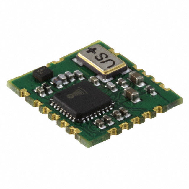
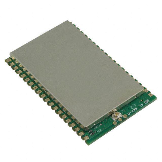
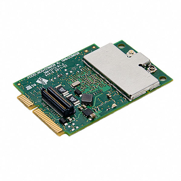
| 描述 | MODULE WIFLY GSX 802.11 B/G U.FL |
| 产品分类 | RF 收发器 |
| 品牌 | Microchip Technology |
| 数据手册 | http://www.microchip.com/mymicrochip/filehandler.aspx?ddocname=en558057http://www.microchip.com/mymicrochip/filehandler.aspx?ddocname=en557989 |
| 产品图片 |
|
| 产品型号 | RN131C/RM |
| PCN制造商信息 | |
| PCN组件/产地 | http://www.microchip.com/mymicrochip/NotificationDetails.aspx?id=6063&print=view |
| PCN设计/规格 | http://www.microchip.com/mymicrochip/NotificationDetails.aspx?id=5655&print=vewhttp://www.microchip.com/mymicrochip/NotificationDetails.aspx?id=5860&print=view |
| rohs | 无铅 / 符合限制有害物质指令(RoHS)规范要求 |
| 产品系列 | - |
| 其它名称 | 740-1036 |
| 其它有关文件 | http://www.microchip.com/mymicrochip/filehandler.aspx?ddocname=en557928 |
| 功率-输出 | 18dBm |
| 包装 | 托盘 |
| 天线连接器 | 板载,芯片,U.FL |
| 存储容量 | 8Mb 闪存,128kB RAM |
| 封装/外壳 | 模块 |
| 工作温度 | 0°C ~ 70°C |
| 应用 | 通用 |
| 数据接口 | PCB,表面贴装 |
| 数据速率(最大值) | 54Mbps |
| 标准包装 | 20 |
| 灵敏度 | -85dBm |
| 电压-电源 | 3 V ~ 3.7 V |
| 电流-传输 | 140mA |
| 电流-接收 | 40mA |
| 调制或协议 | 802.11b/g |
| 频率 | 2.4GHz |


- 商务部:美国ITC正式对集成电路等产品启动337调查
- 曝三星4nm工艺存在良率问题 高通将骁龙8 Gen1或转产台积电
- 太阳诱电将投资9.5亿元在常州建新厂生产MLCC 预计2023年完工
- 英特尔发布欧洲新工厂建设计划 深化IDM 2.0 战略
- 台积电先进制程称霸业界 有大客户加持明年业绩稳了
- 达到5530亿美元!SIA预计今年全球半导体销售额将创下新高
- 英特尔拟将自动驾驶子公司Mobileye上市 估值或超500亿美元
- 三星加码芯片和SET,合并消费电子和移动部门,撤换高东真等 CEO
- 三星电子宣布重大人事变动 还合并消费电子和移动部门
- 海关总署:前11个月进口集成电路产品价值2.52万亿元 增长14.8%


PDF Datasheet 数据手册内容提取
RN-131-DS RN-131G & RN-131C 802.11 b/g Wireless LAN Module Features • Qualified 2.4-GHz IEEE 802.11b/g transceiver • Ultra-low power: 4 uA sleep, 40 mA Rx, 210 mA Tx • High throughput, 1 Mbps sustained data rate with TCP/IP and WPA2 • Small, compact surface-mount module • On-board ceramic chip antenna and U.FL connector for external antenna • 8-Mbit flash memory and 128-KB RAM Description • UART hardware interface • 10 general-purpose digital I/O pins The RN-131 module is a standalone, embedded • 8 analog sensor interfaces wireless 802.11 b/g networking module. With its small form factor and extremely low power consumption, the • Real-time clock for wakeup and time stamping RN-131 is perfect for mobile wireless applications such • Accepts 3.3-V regulated or 2 to 3 V battery as asset monitoring, GPS tracking, and battery sensors. • Supports ad hoc and infrastructure networking The WiFly module incorporates a 2.4-GHz radio, modes processor, TCP/IP stack, real-time clock, crypto • On board ECOS -OS, TCP/IP stacks accelerator, power management, and analog sensor • Wi-Fi Alliance certified for WPA2-PSK interfaces as shown in Figure 1. The module is • FCC/CE/ICS certified and RoHS compliant. preloaded with software to simplify integration and minimize application development. In the simplest • Industrial (RN-131G) and commercial (RN-131C) configuration, the hardware requires only four grade temperature options connections (PWR, TX, RX, and GND) to create a wireless data connection. Additionally, the sensor Applications interface provides temperature, audio, motion, acceleration, and other analog data without requiring • Remote equipment monitoring additional hardware. The module is programmed and • Telemetry controlled with a simple ASCII command language. • Industrial sensors and home automation controls Once the module is set up, it can scan to find an access • Medical device monitoring point, associate, authenticate, and connect over any Wi-Fi network. Figure 1. RN-131 Block Diagram RN-131 On-Board Chip Antenna 128-KB 32-Bit RAM CPU 2-MB ROM Flash 2.4 GHz Memory TX/RX 2.4-GHz Timers Radio 2-K forU O.FpLAti noCntoeannl nnEeaxctteorrnal 2.4-GHz 8M0A2C.1/P1H bY/g B NVM SPI SGPPIIO PA UART VDD IN Crypto Pwr GPIO VDD BATT ADC accelerator Mgmt SDIO 3.3-V Boost Boost Sensor Interface EPC/RFID Regulator Enable www.rovingnetworks.com Version 3.2r 4/9/2012 1
RN-131-DS OVERVIEW • Host data rate up to 1 Mbps for the UART • Intelligent, built-in power management with programmable wakeup • Real-time clock for time stamping, auto-sleep, and auto-wakeup • Configuration over UART using simple ASCII commands • Remote configuration over WiFi using Telnet • Supports over the air firmware upgrade (FTP) • Supports WPS pushbutton mode for easy association with access points • Secure WiFi authentication using WEP-128, WPA-PSK (TKIP), or WPA2-PSK (AES) • Built-in networking applications—DHCP, UDP, DNS, ARP, ICMP, TCP, HTTP client, and FTP client • 802.11 power saving and roaming functions The modules size and weight are: • Size—1.49” x 0.78” x 0.15” (37mm x 20 mm x 3.5 mm) • Weight—0.140 oz Tables 1 through 4 provide detailed specifications for the module. Table 1. Environmental Conditions Parameter RN-131G RN-131C Temperature Range (Operating) -30 oC to +85 oC 0 oC to +70 oC Temperature Range (Storage) -40oC to +85 oC -40oC o +85 oC Relative Humidity (Operating) ≤ 90% ≤ 90% Relative Humidity (Storage) ≤ 90% ≤ 90% Table 2. Electrical Characteristics Supply Voltage Min Typ. Max. Unit Supply voltage VDD 3.0 3.3 3.7 VDC Supply voltage (VBATT option) 2.0 3.0 3.3 VDC Pin 21 switched 3.3 V output 150 mA Digital input Input logic high VIH 2.3 V VDC Input logic low VIL 1.0 V VDC Digital output drive GPIO 4, 5, 6, 7, 8 24 mA GPIO 9, 10, 11, 12, 13 8 mA Power consumption Sleep 4 uA Standby (doze) - 15 - mA Connected (idle, RX) 40 mA Connected (TX) 140 212 mA www.rovingnetworks.com Version 3.2r 4/9/2012 2
RN-131-DS Table 3. Analog Sensor Inputs Parameter Value Sense 0,1,2,3 wakeup detect threshold 500 mV AD sense 0 - 7 measurement range 0 - 400 mV Precision 14 bits = 12 uV Accuracy 5% un-calibrated, 0.01% calibrated Minimum conversion time 35uS (5kHz over Wi-Fi) Sensor Power (pin 33) output resistance 3.3 V 10 ohms, max current = 50 mA Table 4. Radio Characteristics Parameter Specifications Frequency 2,402 to 2,480 MHz 802.11b compatibility: DSSS (CCK-11, CCK-5.5, DQPSK-2, DBPSK-1) Modulation 802.11g: OFDM (default) Channel intervals 5 MHz Channels 1 - 14 Transmission rate (over the air) 1 – 11 Mbps for 802.11b / 6 – 54 Mbps for 802.11g Receive sensitivity -85 dBm typ. Output level (class 1) +18 dBm Maximum RF input to U.FL connector 10 dBm www.rovingnetworks.com Version 3.2r 4/9/2012 3
RN-131-DS TYPICAL APPLICATION SCHEMATIC Figure 2 shows a typical application schematic. Figure 2. Application Schematic P3_3V LED_RED LED_GREEN www.rovingnetworks.com Version 3.2r 4/9/2012 4
RN-131-DS Figure 3 shows the pin pads and Table 5 describes the pins. Figure 3. Pin Pads 44 43 42 41 4039 38 37 36 1 35 2 34 3 33 4 32 5 31 6 30 7 29 8 28 9 27 10 26 11 25 12 24 13 23 14 15 16 17 1819 20 21 22 Top View (Pads Not Visible from Top) Table 5. Pin Description Pin Name Description Default 1 SENSOR 6 Sensor interface, analog input to module, 1.2 V. No connect 2 SENSOR 4 Sensor interface, Analog input to module, 1.2 V. No connect 3 SENSOR 5 Sensor interface, Analog input to module, 1.2 V. No connect 4 SENSOR 7 Analog input to module, 1.2 V. No connect 5 RESET Module reset, active low, reference to VDD-BATT, 160 usec pulse. Pull up 6 EPC-ANT-A EPC port, RFID antenna A. No connect 7 EPC-ANT-B EPC port, RFID antenna B. No connect 8 SUPERCAP Balance center pin voltage on stacked super capacitors, analog 3.3 V. No connect 9 FORCE_AWAKE Force the module to wakeup, input to module, 250 us min. pulse.3.3 V. – 10 GPIO-13 UART RTS flow control, 8-mA drive, 3.3-V tolerant. – 11 GPIO-12 UART CTS flow control, 8-mA drive, 3.3-V tolerant. – 12 UART-RX INPUT: RX in to the module, 3.3-V tolerant. – 13 UART-TX OUTPUT: TX out from the module, 8-mA drive, 3.3-V tolerant. – 14 Not used Not applicable No connect 15 Not used Not applicable No connect 16 Not used Not applicable No connect 17 3.3V-REG-OUT Boost regulator control output, connect to 3.3V-REG-IN to enable. No connect 18 3.3V-REG-IN Boost regulator control input, connect to 3.3V-REG-OUT to enable. GND to disable 19 GND Ground. – 20 VDD-BATT Battery input. 2.0 to 3.3 V with boost regulator in use, otherwise use 3.0 – to 3.7 V. 21 VDD-IN 3.3 to 3.7 voltage. Do not connect when boost regulator is in use. – www.rovingnetworks.com Version 3.2r 4/9/2012 5
RN-131-DS Pin Name Description Default 22 DMA-TX Debug port (apply a 100 kΩ pull down if ultra-low sleep power is High Z required) 23 DMA-RX Debug port No connect 24 GPIO-9 Restore factory resets/enter ad hoc mode, 8-mA drive, 3.3-V tolerant. Input 25 GPIO-8 GPIO, 24-mA drive, 3.3-V tolerant. GP output 26 GPIO-7 GPIO, 24-mA drive, 3.3-V tolerant. GP output 27 GPIO-6 Association STATUS, 24-mA drive, 3.3-V tolerant. LED_RED output 28 GPIO-5 Data transfer STATUS, 24-mA drive, 3.3-V tolerant. LED_YELLOW output 29 GPIO-4 Connection STATUS, 24-mA drive, 3.3-V tolerant. LED_GREEN output 30 SENSOR-1 Sensor interface, analog input to module, 1.2 V. – 31 SENSOR-2 Sensor interface, analog input to module, 1.2 V. – 32 SENSOR-3 Sensor interface, analog input to module, 1.2 V. – 33 SENSE-PWR Voltage output from module to power external sensors, 3.3 V. – 34 SENSOR-0 Wakeup from external condition. – 35 NO CONNECT – No connect 36- GND Must be connected for proper antenna performance. – 44 Figure 4 shows the module’s physical dimensions. Figure 5 shows the pad dimensions. www.rovingnetworks.com Version 3.2r 4/9/2012 6
RN-131-DS Figure 4. Module Physical Dimensions 20 mm 2.5 mm Ceramic Chip Antenna 2.5 mm U.FL Connector 37 mm RN-131 Ceramic Chip RF Shield RF Shield Antenna 3.5 mm Figure 5. Pad Dimensions www.rovingnetworks.com Version 3.2r 4/9/2012 7
RN-131-DS DESIGN CONCERNS The following sections provide information on designing with the RN-131 module, including radio interference, grounding, solder reflow, connection status, etc. Minimizing Radio Interference When integrating the WiFly module with the on-board chip antenna, ensure that the area around the chip antenna end of the module protrudes at least 6 mm from the motherboard and any metal enclosure. If this placement is not possible, use the on-board U.FL connector to route to an external antenna. The 8.5-mm area under the module’s antenna end should be kept clear of metallic components, connectors, vias, traces, and other materials that can interfere with the radio signal. See Figure 6. Figure 6. Antenna Clearance 20 mm 6 mm Keep Metallic Components, Connectors, Vias, & Traces Away from Antenna Area 8.5 mm RN-131 Top View www.rovingnetworks.com Version 3.2r 4/9/2012 8
RN-131-DS Grounding Recommendations For the module antenna to function, pins 36 through 44 must be connected to ground. Roving Networks suggests you place the module such that 0.5 mm of theses pads is exposed. This placement provides access for soldering pins 36 through 44 from below, and provides ample clearance of the antenna from the PCB. See Figure 7. Figure 7. Module Placement for Grounding 8.5 mm For Proper Antenna Performance, Pins 36 Through 44 Must be Grounded RN-131 Motherboard for RN-131 Bottom View Solder Reflow The solder reflow temperature must not exceed 220° C. To reflow solder the module onto a PCB, Roving Networks recommends an RoHS-compliant solder paste equivalent to NIHON ALMIT paste or OMNIX OM-310 solder paste from Alpha metals. See Table 6. NOTE: Use no-clean flux and DO NOT water wash. Table 6. Paste Solder Recommendations Manufacturer Alpha Metals NIHON ALMIT Co. LTD http://www.alphametals.com http://almit.co.jp Part Number OMNIX OM-310 LFM-70W INP Metal Composition SAC305 (96.5% Sn, 3% Ag, 0.5% Cu) 88% Sn, 3.5% Ag, 0.5% Bi, 8% In Liquidus Temperature ~220°C ~215°C Figures 8 and 9 show the solder reflow temperature profiles. www.rovingnetworks.com Version 3.2r 4/9/2012 9
RN-131-DS Figure 8. Solder Reflow Temperature Profile www.rovingnetworks.com Version 3.2r 4/9/2012 10
RN-131-DS Figure 9. Solder Reflow Curve U.FL Connector Roving Networks recommends that you use the Hirose U.FL connector (part number U.FL-R-SMT) for connecting external antennas. If you prefer to use the SMA connector, use the Roving Networks U.FL-to-SMA cable (part number RN-UFLSMA6). Figure 10 shows the U.FL connector dimensions. Figure 10. U.FL Connector Dimensions www.rovingnetworks.com Version 3.2r 4/9/2012 11
RN-131-DS Connection Status GPIO4, GPIO5, and GPIO6 drive status the LEDs. • GPIO4 indicates the TCP/IP connection status. This signal is on high for an active connection, toggles fast to indicate no IP address, and toggles slowly to indicate that the IP address is OK but not connected. • GPIO6 indicates the association status. High means the module is not associated with a network, off indicates that it is associated and Internet access is OK. • GPIO5 toggles when data is transferred. Keep-Out Areas When designing your PCB avoid exposed traces and vias beneath the module. Figure 11 shows areas on the module that should be kept clear. Figure 11. Keep Out Areas Keep Out Areas. There are two 1-mm round test pads on the bottom of the module. Avoid placing exposed traces or vias in these areas. 8.0 mm 3 mm 6 mm 5 mm Powering the Module The module can be powered from either 3.0-V DC batteries or 3.3-V DC regulated power. For 3.0-V DC battery power: • Apply power to pin 20 (VDD-BATT). • Short pin 17 (3.3 V REG-OUT) to pin 18 (3.3 V REG-IN) (battery boost mode). • 150 mA of current at 3.3 V is available for external devices on pin 21 when the module is in battery boost mode. For 3.3-V DC power: • Apply power to pin 20 (VDD-BATT) and pin 21 (VDD-IN). • Connect pin 18 (3.3 V REG-IN) to ground and leave pin 17 (3.3 V REG-OUT) unconnected. www.rovingnetworks.com Version 3.2r 4/9/2012 12
RN-131-DS Reset (Pin 5) The RESET signal is used to reset the module and is active low. This pin has a built-in 100-kΩ pull up resistor. You do not need to connect this; it can be left unconnected. To reset the module, apply a 3.3-V pulse for a minimum of 160 us. Force Awake (Pin 9) This signal forces the module to wake up from sleep. FORCE_AWAKE is an active-high signal. To wake the module, apply a 3.3-V pulse for a minimum of 250 us. Achieving Lowest Power in Sleep Mode To achieve the lowest power consumption (4 uA) in sleep mode, connect a weak pull-down (100 KΩ resistor to GND) on pin 22 (DMA-TX). If GPIO8 through GPIO4 are being used to drive an output, connect a 100-kΩ pull-down resistor. Any unused (no connect) GPIO pins can be left floating. • Pin 25: GPIO8 • Pin 26: GPIO7 • Pin 27: GPIO6 • Pin 28: GPIO5 • Pin 29: GPIO4 For other GPIO lines, you do not need to use a pull down. The module already has an on-chip internal pull down (80 kΩ); The power consumption in sleep mode without these signals connected to a pull down is 655 uA. Sensor Interfaces Inputs must not exceed 1.2 V. The sensitivity saturates at 400 mV. Ad Hoc Mode & Restoring Factory Settings Ad hoc mode is controlled with GPIO9 (pin 24). Roving Networks recommends that you connect pin 24 to a switch or jumper connected to a pull up. When GPIO9 is driven high at power up, the module enters ad hoc mode. If GPIO9 is then toggled low 5 times, the module will be restored to it’s initial factory default configuration. This feature is useful for cases where the module is misconfigured and is no long responding. www.rovingnetworks.com Version 3.2r 4/9/2012 13
RN-131-DS COMPLIANCE INFORMATION The following sections describe the module’s FCC and NCC compliance information. FCC Compliance This equipment has been tested and found to comply with the limits for a Class digital device, pursuant to Part 15 of the FCC rules. These limits are designed to provide reasonable protection against harmful interference in a residential installation. This equipment generates uses and can radiate radio frequency energy and, if not installed and used in accordance with the instructions, may cause harmful interference to the radio communications. However, there are no guarantees that interference will not occur in a particular installation. Troubleshooting If this equipment does cause harmful interference to radio or television reception, which can be determined by turning the equipment off and on, the user is encouraged to try to correct the interference by one or more of the following instructions • Reorient or relocate the receiving antenna. • Increase the separation between the equipment and receiver. • Connect the equipment to an outlet or a circuit difference from that to which the receiver is connected. • Consult the dealer or an experienced radio/TV technician. Conditions Operation is subject to the following conditions • This device may not cause harmful interference. • This device must accept any interference received, including interference that may cause undesired operation. Markings To satisfy the FCC exterior labeling requirements the following text must be placed on the exterior of the end product. Contains Module FCC ID: U30-G2M5477 This marking applies to the G2M5477 and the RN-131 module, which are the same. Any similar working that expresses the same meaning may be used. FCC Warning Modifications Modifications not expressly approved by the manufacturer could void the user’s authority to operate the equipment under FCC rules. See Table 7. www.rovingnetworks.com Version 3.2r 4/9/2012 14
RN-131-DS Table 7. Radio Frequency Exposure Property (Units Measured) Value Units Antenna Gain 2.0 dBi Numeric Gain 1.58 Numeric Max Allowable Peak Power +23.76 dBm Max Allowable Peak Power 237.7 mW Calculated Safe Distance at 1 5.5 mW/cm2 Minimum Separation Distance 20 cm3 This equipment has been evaluated in accordance with the FCC bulletin 56 “Hazards of radio frequency and electromagnetic fields” and Bulletin 65 “Human exposure to radio frequency and electromagnetic fields.” A distance greater or equal to 20 cm from the device should be maintained for safe operation in an uncontrolled environment. NCC (Taiwan Statement) Contains Transmitter Module NCC ID: CCAF11LP0240T6 802.11b/802.11g/BT 警語: 第十二條→經型式認證合格之低功率射頻電機,非經許可,公司,商號或使用者均不得擅自變更頻率、加 大功率或變更原設計之特性及功能。 第十四條→低功(cid:0)射頻電機之使用(cid:0)得影響飛航安全及干擾合法通信;經發現有干擾現象時,應(cid:0)即停用 ,並改善至無干擾時方得繼續使用。 前項合法通信,指依電信法規定作業之無線電通信。 低功(cid:0)射頻電機須忍受合法通信或工業、科學及醫(cid:0) 用電波(cid:0)射性電機設備之干擾。 Unofficial Translation Article 12 Without permission granted by the NCC, any company, enterprise, or user is not allowed to change frequency, enhance transmitting power or alter original characteristic as well as performance to an approved low power radio-frequency devices. Article 14 The low power radio-frequency devices shall not influence aircraft security and interfere legal communications. If found, the user shall cease operating immediately until no interference is achieved. The said legal communications means radio communications is operated in compliance with the Telecommunications Act. The low power radio-frequency devices must be susceptible with the interference from legal communications or ISM radio wave radiated devices. www.rovingnetworks.com Version 3.2r 4/9/2012 15
RN-131-DS Table 8. Compliance Information Specification Compliance FCC ID U3O-G2M5477 Part 15.247 IC (Canada) RSS-210 CE EU ID # 0681 REG U9M20901-1000-C RADIO EN 300328 V1.7.1 (10/2006) EMC EN 301489-1 V1.8.1 (04/2008), EN 301489-17 V1.3.2 (04/2008) SAFETY EN 60950-1:2001+A11:2004 RoHs Compliant ORDERING INFORMATION Table 9 provides ordering information. Table 9. Ordering Information Part Number Description RN-131G Industrial Temperature (-30 to + 85 C ) With chip antenna and U.FL connector RN-131C Commercial Temperature (0 to + 70 C ) With chip antenna and U.FL connector RN-131G-EVAL Development Kit for the RN-131G (Includes the RN-131G module) RN-134 RN-131 Evaluation board, includes RS-232, LEDs, and power regulator. Sensor connections. RN-SMA4-RP 4” external antenna with reverse polarity SMA connector. Used with RN-UFL-SMA6 RN-UFL-SMA6 6 inch cable with U.FL connector on one end and SMA on the other For other configurations, contact Roving Networks directly. Go to http://www.rovingnetworks.com for current pricing and a list of distributors carrying Roving Networks products. www.rovingnetworks.com Version 3.2r 4/9/2012 16
RN-131-DS NOTES www.rovingnetworks.com Version 3.2r 4/9/2012 17
RN-131-DS Copyright © 2012 Roving Networks. All rights reserved. Roving Networks is a registered trademark of Roving Networks. Apple Inc., iPhone, iPad, iTunes, Made for iPhone are registered trademarks of Apple Computer. Roving Networks reserves the right to make corrections, modifications, and other changes to its products, documentation and services at any time. Customers should obtain the latest relevant information before placing orders and should verify that such information is current and complete. Roving Networks assumes no liability for applications assistance or customer’s product design. Customers are responsible for their products and applications which use Roving Networks components. To minimize customer product risks, Roving Networks, Inc. customers should provide adequate design and operating safeguards. 102 Cooper Court Roving Networks products are not authorized for use in safety-critical applications Los Gatos, CA 95032 (such as life support) where a failure of the Roving Networks product would +1 (408) 395-5300 reasonably be expected to cause severe personal injury or death, unless officers of www.rovingnetworks.com the parties have executed an agreement specifically governing such use. www.rovingnetworks.com Version 3.2r 4/9/2012 18