 Datasheet下载
- 型号: RCLAMP0524J.TCT
- 制造商: SEMTECH
- 库位|库存: xxxx|xxxx
- 要求:
| 数量阶梯 | 香港交货 | 国内含税 |
| +xxxx | $xxxx | ¥xxxx |
查看当月历史价格
查看今年历史价格
RCLAMP0524J.TCT产品简介:
ICGOO电子元器件商城为您提供RCLAMP0524J.TCT由SEMTECH设计生产,在icgoo商城现货销售,并且可以通过原厂、代理商等渠道进行代购。 RCLAMP0524J.TCT价格参考¥3.10-¥8.04。SEMTECHRCLAMP0524J.TCT封装/规格:TVS - 二极管, 15V Clamp 5A (8/20µs) Ipp Tvs Diode Surface Mount SLP2710P8。您可以下载RCLAMP0524J.TCT参考资料、Datasheet数据手册功能说明书,资料中有RCLAMP0524J.TCT 详细功能的应用电路图电压和使用方法及教程。
RCLAMP0524J.TCT是Semtech Corporation生产的一款瞬态电压抑制(TVS)二极管,属于低电容、高可靠性保护器件。该器件主要用于电子设备中对敏感电路进行静电放电(ESD)和浪涌电压的防护。

其典型应用场景包括:便携式消费类电子产品(如智能手机、平板电脑、笔记本电脑)、USB接口保护(特别是USB 2.0和USB 3.0高速数据线)、HDMI接口、音频/视频端口、SIM卡接口以及其它高速数据通信线路。由于其超低电容(通常低于1pF),能够有效保护信号完整性,适用于高速数据传输场景,避免因寄生电容影响信号质量。

RCLAMP0524J.TCT具备快速响应时间(皮秒级)和高脉冲功率承受能力,可有效钳制瞬态过电压,将残压限制在安全范围内,从而保护后级集成电路。其工作电压为5V,适合用于低压电源轨和I/O端口的保护。

此外,该器件采用小型化封装(如SOD-882),节省PCB空间,适用于高密度布局的现代电子产品。广泛应用于工业控制、通信设备、汽车电子外围接口及家用电器中需要可靠ESD和浪涌保护的场合。

综上,RCLAMP0524J.TCT是一款高性能TVS二极管,特别适用于高速信号线和低压电路的电磁兼容(EMC)防护,确保电子系统在恶劣电气环境下的稳定运行。
| 参数 | 数值 |
| 产品目录 | |
| 描述 | TVS DIODE 5VWM 15VC 8SLP |
| 产品分类 | |
| 品牌 | Semtech |
| 数据手册 | |
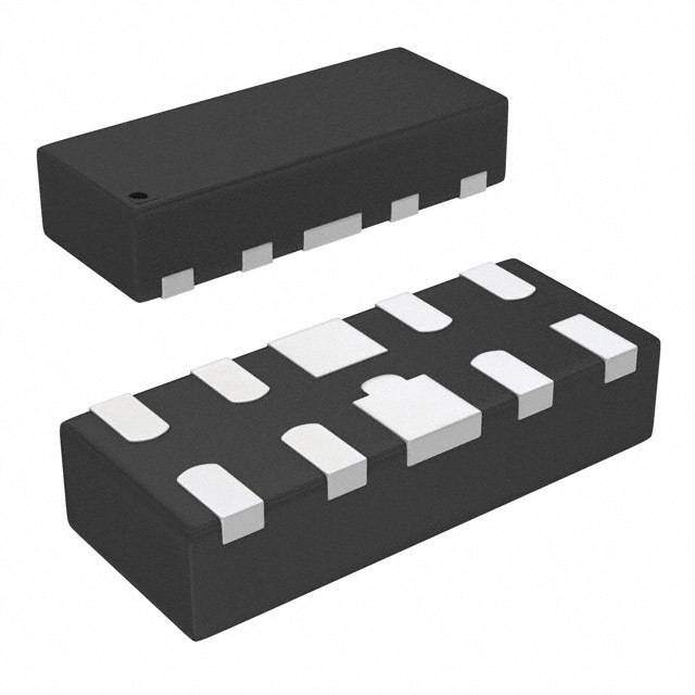
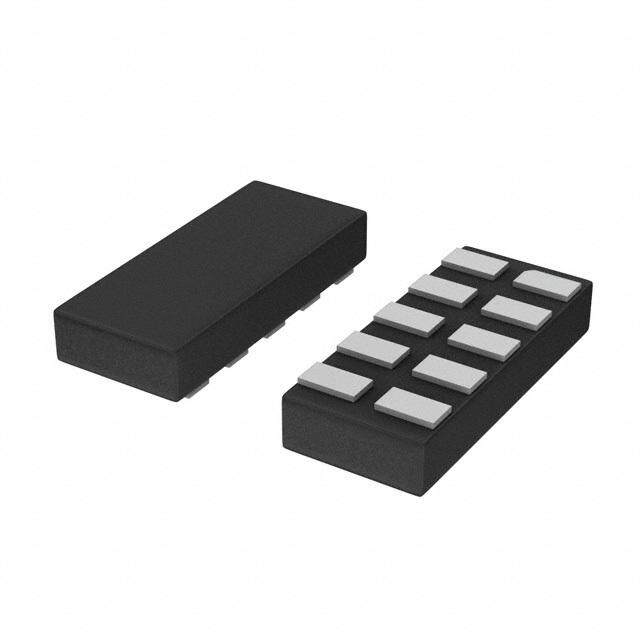
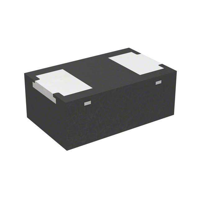
| 产品图片 |
|
| 产品型号 | RCLAMP0524J.TCT |
| rohs | 无铅 / 符合限制有害物质指令(RoHS)规范要求 |
| 产品系列 | RailClamp® |
| 不同频率时的电容 | 0.8pF @ 1MHz |
| 产品目录页面 | |
| 供应商器件封装 | SLP2710P8 |
| 其它名称 | RCLAMP0524JTCT |
| 功率-峰值脉冲 | 150W |
| 包装 | 带卷 (TR) |
| 单向通道 | - |
| 双向通道 | 4 |
| 安装类型 | 表面贴装 |
| 封装/外壳 | 10-SMD,无引线 |
| 工作温度 | -55°C ~ 125°C (TJ) |
| 应用 | HDMI |
| 应用说明 | |
| 标准包装 | 3,000 |
| 电压-击穿(最小值) | 6V |
| 电压-反向关态(典型值) | 5V(最小值) |
| 电压-箝位(最大值)@Ipp | 15V |
| 电流-峰值脉冲(10/1000µs) | 5A (8/20µs) |
| 电源线路保护 | 是 |
| 类型 | 转向装置(轨至轨) |


- 商务部:美国ITC正式对集成电路等产品启动337调查
- 曝三星4nm工艺存在良率问题 高通将骁龙8 Gen1或转产台积电
- 太阳诱电将投资9.5亿元在常州建新厂生产MLCC 预计2023年完工
- 英特尔发布欧洲新工厂建设计划 深化IDM 2.0 战略
- 台积电先进制程称霸业界 有大客户加持明年业绩稳了
- 达到5530亿美元!SIA预计今年全球半导体销售额将创下新高
- 英特尔拟将自动驾驶子公司Mobileye上市 估值或超500亿美元
- 三星加码芯片和SET,合并消费电子和移动部门,撤换高东真等 CEO
- 三星电子宣布重大人事变动 还合并消费电子和移动部门
- 海关总署:前11个月进口集成电路产品价值2.52万亿元 增长14.8%


PDF Datasheet 数据手册内容提取
RClamp0524J RailClamp®®®®® Ultra Low Capacitance TVS Arrays ®®®®® PPRROOTTEECCTTIIOONN PPRROODDUUCCTTSS - RailClamp PRELIMINARY Description Features RailClamps® are ultra low capacitance TVS arrays (cid:139) ESD protection for high-speed data lines to designed to protect high speed data interfaces. This IEC 61000-4-2 (ESD) ±15kV (air), ±8kV (contact) series has been specifically designed to protect sensitive IEC 61000-4-5 (Lightning) 5A (8/20μs) components which are connected to high-speed data IEC 61000-4-4 (EFT) 40A (5/50ns) and transmission lines from overvoltage caused by ESD (cid:139) Package design optimized for high speed lines (electrostatic discharge), CDE (Cable Discharge Events), (cid:139) Flow-Through design and EFT (electrical fast transients). (cid:139) Protects four I/O lines The RClampTM0524J has a typical capacitance of only (cid:139) Low capacitance: 0.3pF typical (I/O to I/O) 0.30pF between I/O pins. This allows it to be used on (cid:139) Low clamping voltage circuits operating in excess of 3GHz without signal (cid:139) Low operating voltage: 5V attenuation. They may be used to meet the ESD (cid:139) Solid-state silicon-avalanche technology immunity requirements of IEC 61000-4-2, Mechanical Characteristics Level 4 (±15kV air, ±8kV contact discharge). Each device is designed to protect four lines (two differential (cid:139) SLP2710P8 8-pin package (2.7 x 1.0 x 0.5mm) pairs). (cid:139) RoHS/WEEE Compliant The RClamp0524J is in a 8-pin, RoHS/WEEE compliant, (cid:139) Lead Pitch: 0.5mm SLP2710P8 package. It measures 2.7 x 1.0 x 0.5mm. (cid:139) Lead finish: NiPdAu The leads are spaced at a pitch of 0.5mm and are fin- (cid:139) Marking: Marking Code ished with lead-free NiPdAu. They are designed for easy (cid:139) Packaging: Tape and Reel per EIA 481 PCB layout by allowing the traces to run straight through the device. The combination of small size, low capaci- tance, and high level of ESD protection makes them a Applications flexible solution for applications such as HDMI, (cid:139) High Definition Multi-Media Interface (HDMI) DisplayPortTM, MDDI, and eSATA interfaces. (cid:139) Digital Visual Interface (DVI) (cid:139) DisplayPortTM Interface (cid:139) MDDI Ports (cid:139) LVDS (cid:139) Serial ATA (cid:139) PCI Express Dimensions Circuit Diagram 2.70 0.40 1 2 1.00 Pin 1 Pin 2 Pin 3 Pin 4 0.60 0.20 0.50 GND 0.50 Nominal Dimensions in mm 4-Line Protection Revision 07/20/2010 1 www.semtech.com
RClamp0524J PROTECTION PRODUCTS PRELIMINARY Absolute Maximum Rating Rating Symbol Value Units PeakPulsePower (tp = 8/20μs) P 150 Watts pk PeakPulseCurrent(tp = 8/20μs) I 5 A PP ESD per IEC 61000-4-2 (Air) V +/- 17 kV ESD ESD per IEC 61000-4-2 (Contact) +/- 12 Operating Temperature T -55 to+125 °C J StorageTemperature T -55 to+150 °C STG Electrical Characteristics (T=25oC) Parameter Symbol Conditions Minimum Typical Maximum Units ReverseStand-Off Voltage V Any I/Opin toground 5 V RWM ReverseBreakdown Voltage V I =1mA 6 V BR t Any I/Opin toground ReverseLeakageCurrent I V =5V, T=25°C 1 μA R RWM Any I/Opin toground Clamping Voltage V I =1A, tp =8/20μs 15 V C PP Any I/Opin toground V =0V, f =1MHz 0.30 0.4 pF Junction Capacitance C R j Between I/Opins V =0V, f =1MHz 0.8 pF Junction Capacitance C R j Any I/Opin toground © 2011 Semtech Corp. 2 www.semtech.com
RClamp0524J PROTECTION PRODUCTS PRELIMINARY Typical Characteristics Non-Repetitive Peak Pulse Power vs. Pulse Time Power Derating Curve 10 110 100 W) 90 wer - P (kPP 1 Power or IPP 678000 ak Pulse Po 0.1 % of Rated 345000 Pe 20 10 0.01 0 0.1 1 10 100 1000 0 25 50 75 100 125 150 Pulse Duration - tp (us) Ambient Temperature - T (oC) A Pulse Waveform Clamping Voltage vs. Peak Pulse Current 110 Waveform 40 100 Parameters: 90 35 tr = 8µs 80 td = 20µs V) 30 (C Line to Line ent of IPP 567000 e-t Voltage -V 2205 Line to Gnd Perc 40 td = IPP/2 mping 15 30 Cla 10 PWaraavmefeotremrs: 20 tr = 8µs 5 10 td = 20µs 0 0 0 1 2 3 4 5 6 0 5 10 15 20 25 30 Peak Pulse Current - I (A) PP Time (µs) Normalized Capacitance vs. Reverse Voltage ESD Clamping for +8kV pulse per IEC 61000-4-2 1.5 1.4 1.3 1.2 1.1 1 =0) 0.9 R V 0.8 C(J 0.7 ) / R 0.6 V C(J 0.5 0.4 0.3 0.2 0.1 f = 1 MHz 0 0 1 2 3 4 5 Reverse Voltage - V (V) R © 2011 Semtech Corp. 3 www.semtech.com
RClamp0524J PROTECTION PRODUCTS PRELIMINARY Typical Characteristics (Con’t) Insertion Loss S21 - I/O to I/O Insertion Loss S21 - I/O to GND CH1 S21 LOG 6 dB / REF 0 dB CH1 S21 LOG 6 dB / REF 0 dB 1: -0.076 dB 1: -0.086 dB 900 MHz 900 MHz 3 2: -0.062 dB 3 2: -0.0336 dB 0 dB 1.8 GHz 0 dB 1.8 GHz 1 2 1 2 -6 dB 3: -0.1087 dB -6 dB 3: -0.126 dB 2.5 GHz 2.5 GHz -12 dB -12 dB -18 dB -18 dB -24 dB -24 dB -30 dB -30 dB -36 dB -36 dB -42 dB -42 dB -48 dB -48 dB 1 10 100 1 3 1 10 100 1 3 MHz MHz MHz GHz GHz MHz MHz MHz GHz GHz START . 030 MHz STOP 3 000. 0000 00 MHz START . 030 MHz STOP 3 000. 0000 00 MHz © 2011 Semtech Corp. 4 www.semtech.com
RClamp0524J PROTECTION PRODUCTS PRELIMINARY Applications Information 8 7 GND 6 5 Design Recommendations for HDMI Protection Adding external ESD protection to HDMI ports can be challenging. First ESD protection devices have an inherent junction capacitance. However, adding even a small amount of capacitance will cause the impedance of the differential pair to drop. Second, large packages 1 2 GND 3 4 and land pattern requirements cause discontinuities that adversely affect signal integrity. The RClamp0524J is specifically designed for protection of Pin Identification high-speed interfaces such as HDMI. They present <0.3pF capacitance between the pairs while being 1,2,3,4 Input Lines rated to handle >±8kV ESD contact discharges (>±15kV air discharge) as outlined in IEC 61000-4-2. Output Lines 5,6,7,8 (NoInternal Connection) Each device is in a leadless SLP package that is less than 1.1mm wide. They are designed such that the GND Ground traces flow straight through the device. The narrow package and flow-through design reduces discontinuities and minimizes impact on signal integrity. SLP2710P8 Pin Configuration (Top View) This becomes even more critical as signal speeds increase. Pin Configuration Figure 1 is an example of how to route the high speed differential traces through the RClamp0524J. The solid line represents the PCB trace. The PCB traces are used to connect the pin pairs for each line (pin 1 to pin 8, pin 2 to pin 7, pin 3 to pin 6, pin 4 to pin 5). For 1 1122 example, line 1 enters at pin 1 and exits at Pin 8 and 1111 the PCB trace connects pin 1 and 8 together. This is 1100 true for lines connected at pins 2, 3, and 4 also. GND GND rr Ground is connected at the center tabs. One large oo 99 tt ground pad should be used in lieu of two separate cc 88 ee nn 77 pads. nn oo 1 CC TDR Measurements for HDMI I I 66 MM 55 The combination of low capacitance, small package, and DD 44 HH flow-through design means it is possible to use these GND GND devices to meet the HDMI impedance requirements of 33 100 Ohm ±15% without any PCB board modification. 22 11 Figures 3 and 4 show impedance test results for a TDR risetime of 200ps and 100ps respectively, using a Semtech evaluation board with 100 Ohm traces through- FFFFFiiiiiggggguuuuurrrrreeeee 11111..... FFFFFlllllooooowwwww ttttthhhhhrrrrrooooouuuuuggggghhhhh LLLLLaaaaayyyyyooooouuuuuttttt UUUUUsssssiiiiinnnnnggggg out. Measurements were taken using a TDR method as RRRRRCCCCClllllaaaaammmmmppppp00000555552222244444JJJJJ outlined in the HDMI Compliance Test Specification (CTS). In each case, the device meets the HDMI CTS © 2011 Semtech Corp. 5 www.semtech.com
RClamp0524J PROTECTION PRODUCTS PRELIMINARY Applications Information requirement of 100 Ohm ±15% with plenty of margin. For signal integrity purposes, the best results will be obtained by using the RClamp0524J to protect the high-speed differential pairs. This is because the BB device is designed such that the data lines from the connector line up with the I/O pins of the device without altering the trace routing. Either the RClamp0504P or RClamp0524J may be used to AA protect the remaining lines (I2C, CEC, and hot plug) depending on layout constraints. Layout Guidelines for Optimum ESD Protection Good circuit board layout is critical not only for signal integrity, but also for effective suppression of ESD in- duced transients. For optimum ESD protection, the A B following guidelines are recommended: X-axis 1.905 2.081 (nsec) (cid:122) Place the device as close to the connector as pos- Y-axis 101.0 107.0 (Ohm) sible. This practice restricts ESD coupling into adjacent traces and reduces parasitic inductance. Figure 2 - TDR Measurement with 200ps risetime (cid:122) The ESD transient return path to ground should be using Semtech Evaluation Board kept as short as possible. Whenever possible, use multiple micro vias connected directly from the device ground pad to the ground plane. (cid:122) Avoid running critical signals near board edges. BB AA A B X-axis 1.80 2.076 (nsec) Y-axis 96 108.0 (Ohm) Figure 3 - TDR Measurement with 100ps risetime using Semtech Evaluation Board Note: Measurements were taken on SLP HDMI EVAL Rev C Board that has 100Ω differential traces impedance throughout (No trace Compensation). © 2011 Semtech Corp. 6 www.semtech.com
RClamp0524J PROTECTION PRODUCTS PRELIMINARY Applications Information RRCCllaammpp00552244JJ DDaattaa 22++ DDaattaa 22-- DDaattaa 11++ DDaattaa 11-- TToo HHDDMMII DDaattaa 00++ GGrraapphhiiccss CChhiipp DDaattaa 00-- CCllkk++ CCllkk-- RRCCllaammpp00552244JJ CCEECC SSCCLL SSDDAA GGnndd 55VVPPoowweerr HHPP DDeetteecctt 111 666 RRCCllaammpp00550044PP FFFFFiiiiiggggguuuuurrrrreeeee 44444..... HHHHHDDDDDMMMMMIIIII PPPPPrrrrrooooottttteeeeeccccctttttiiiiiooooonnnnn EEEEExxxxxaaaaammmmmpppppllllleeeee HHH EEE ooo SSS HHHHHHoooooosssssstttttt TTTTTTxxxxxx+-+-+- AAAA ++-- st Plust Plust Plu ATAATAATA ggg HHHooosssttt RRRxxx --- BBB --- HHHooosssttt RRRxxx +++ BBB +++ 11 RRCCllaammpp00552244JJ 11 AA ++ AA -- e e cc vivi ee DD A A BBBBBB ------ TT AAgg BBBBBB +++--- SSuu EEPlPl RRCCllaammpp00552244JJ FFFFFiiiiiggggguuuuurrrrreeeee 55555..... eeeeeSSSSSAAAAATTTTTAAAAA PPPPPrrrrrooooottttteeeeeccccctttttiiiiiooooonnnnn EEEEExxxxxaaaaammmmmpppppllllleeeee © 2011 Semtech Corp. 7 www.semtech.com
RClamp0524J PROTECTION PRODUCTS PRELIMINARY Applications Information 11111 RRRCCClllaaammmppp000555222444JJJ DDDDDDDDDDDDIIIIIIIIIIIISSSSSSSSSSSSPPPPPPPPPPPPLLLLLLLLLLLLAAAAAAAAAAAAYYYYYYYYYYYY PPPPPPPPPPPPOOOOOOOOOOOORRRRRRRRRRRRTTTTTTTTTTTT CCCCCCCCCCCCOOOOOOOOOOOONNNNNNNNNNNNNNNNNNNNNNNNEEEEEEEEEEEECCCCCCCCCCCCTTTTTTTTTTTTOOOOOOOOOOOORRRRRRRRRRRR 11111 RRRCCClllaaammmppp000555222444JJJ 11111 RRRCCClllaaammmppp000555222444JJJ OOOOOOOOOhhhhhhhhhmmmmmmmmm μμμμμμμμμ FFFFFiiiiiggggguuuuurrrrreeeee 66666..... DDDDDiiiiisssssppppplllllaaaaayyyyyPPPPPooooorrrrrttttt PPPPPrrrrrooooottttteeeeeccccctttttiiiiiooooonnnnn EEEEExxxxxaaaaammmmmpppppllllleeeee © 2011 Semtech Corp. 8 www.semtech.com
RClamp0524J PROTECTION PRODUCTS PRELIMINARY Applications Information Spice Model RClamp0524J Spice Model RClamp0524JSpice Parameters Parameter Unit D1(LCRD) D2(LCRD) D3(TVS) IS Amp 1E-20 1E-20 2E-12 BV Volt 100 100 9.36 VJ Volt 0.7 0.7 0.6 RS Ohm 0.458 1.0 2.6 IBV Amp 1E-3 1E-3 1E-3 CJO Farad 0.4E-12 0.6E-12 56E-12 TT sec 2.541E-9 2.541E-9 2.541E-9 M -- 0.01 0.01 0.23 N -- 1.1 1.1 1.1 EG eV 1.11 1.11 1.11 © 2011 Semtech Corp. 9 www.semtech.com
RClamp0524J PROTECTION PRODUCTS PRELIMINARY OOuuttlliinnee DDrraawwiinngg -- SSOL-P82710P8 A D B DIMENSIONS MILLIMETERS DIM MIN NOMMAX A 0.47 0.50 0.53 A1 0.00 0.03 0.05 PIN 1 E A2 (0.13) INDICATOR b 0.15 0.20 0.25 (LASER MARK) b1 0.35 0.40 0.45 D 2.60 2.70 2.80 E 0.90 1.00 1.10 e 0.50 BSC e1 0.60 BSC L 0.30 0.38 0.43 A N 8 SEATING aaa 0.08 aaa C PLANE bbb 0.10 A2 A1 C b1xN R0.125 bbb C A B 1 2 E/2 LxN 2X R0.075 7 PLACES N e1 bxN e bbb C A B D/2 NOTES: 1. CONTROLLING DIMENSIONS ARE IN MILLIMETERS (ANGLES IN DEGREES). Land Pattern - SLP2710P8 P1 P DIMENSIONS DIM INCHES MILLIMETERS Y C (.034) (0.875) G .008 0.20 Z (C) G (Y1) P .020 0.50 P1 .024 0.60 X .008 0.20 X1 .016 0.40 Y .027 0.675 X Y1 (.061) (1.55) X1 Z .061 1.55 NOTES: 1. CONTROLLING DIMENSIONS ARE IN MILLIMETERS (ANGLES IN DEGREES). 2. THIS LAND PATTERN IS FOR REFERENCE PURPOSES ONLY. CONSULT YOUR MANUFACTURING GROUP TO ENSURE YOUR COMPANY'S MANUFACTURING GUIDELINES ARE MET. © 2011 Semtech Corp. 10 www.semtech.com
RClamp0524J PROTECTION PRODUCTS PRELIMINARY Marking Codes Ordering Information Number Qtyper Reel Part Number 0524J ofLines Reel Size PIN 1 RClamp0524J.TCT 4 3000 7Inch INDICATOR YYWW Note: Lead finish is lead-free NiPdAu. YYWW = Date Code Tape and Reel Specification Pin 1 Location User Direction of feed Device Orientation in Tape PartNumber A0 B0 K0 RClamp0524J 1.21+/-0.10mm 2.91+/-0.10mm 0.66+/-0.10mm Tape K B,(Max) D D1 E F P P0 P2 T(MAX) W Width (MAX) 8.0mm 0.5mm 1.750±.10 1.5+0.1mm 3.5±0.05 4.0±0.1 4.0±0.1 2.0±0.05 +0.3mm 8mm 4.2mm ±0.05 mm 2.4mm 0.4mm -0.0mm) mm mm mm mm -0.1mm Contact Information Semtech Corporation Protection Products Division 200 Flynn Road, Camarillo, CA 93012 Phone: (805)498-2111 FAX (805)498-3804 © 2011 Semtech Corp. 11 www.semtech.com