ICGOO在线商城 > 电阻器 > 芯片电阻 - 表面安装 > RCL12251K00JNEG
 Datasheet下载
- 型号: RCL12251K00JNEG
- 制造商: Vishay
- 库位|库存: xxxx|xxxx
- 要求:
| 数量阶梯 | 香港交货 | 国内含税 |
| +xxxx | $xxxx | ¥xxxx |
查看当月历史价格
查看今年历史价格
RCL12251K00JNEG产品简介:
ICGOO电子元器件商城为您提供RCL12251K00JNEG由Vishay设计生产,在icgoo商城现货销售,并且可以通过原厂、代理商等渠道进行代购。 RCL12251K00JNEG价格参考。VishayRCL12251K00JNEG封装/规格:芯片电阻 - 表面安装, 1 kOhms ±5% 2W Chip Resistor Wide 2512 (6432 Metric), 1225 Automotive AEC-Q200 Thick Film。您可以下载RCL12251K00JNEG参考资料、Datasheet数据手册功能说明书,资料中有RCL12251K00JNEG 详细功能的应用电路图电压和使用方法及教程。
Vishay Dale的RCL12251K00JNEG是一款高精度、高稳定性的表面贴装芯片电阻,属于RCL系列,具有优异的长期稳定性与抗湿性,适用于对性能要求严苛的精密电子设备。其典型应用场景包括:工业控制设备中的精密测量电路、医疗电子设备(如监护仪、诊断设备)中的信号调理模块、测试与测量仪器(如万用表、示波器)中的分压和反馈网络,以及高端通信设备中的模拟前端电路。该电阻阻值为1.00kΩ,精度达±5%,工作温度范围宽(-55°C至+155°C),具备良好的耐高温和抗老化性能,适合在恶劣环境或长期运行系统中使用。此外,由于其符合AEC-Q200标准,也可用于部分汽车电子应用,如传感器模块和车载控制单元。RCL12251K00JNEG采用1225封装尺寸(3.2mm × 6.4mm),功率可达1W,适合需要较高功率密度和散热能力的设计。总体而言,该器件广泛应用于需高可靠性、高精度和长期稳定性的高端电子系统中。
| 参数 | 数值 |
| 产品目录 | |
| 描述 | RES 1K OHM 2W 5% 1225 WIDE厚膜电阻器 - SMD 2watt 1Kohm 5% 200ppm 1225 |
| 产品分类 | |
| 品牌 | Vishay DaleVishay / Draloric |
| 产品手册 | |
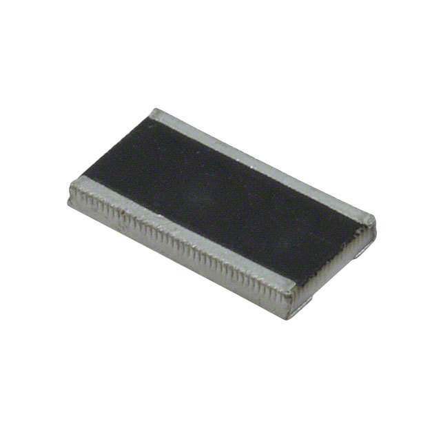
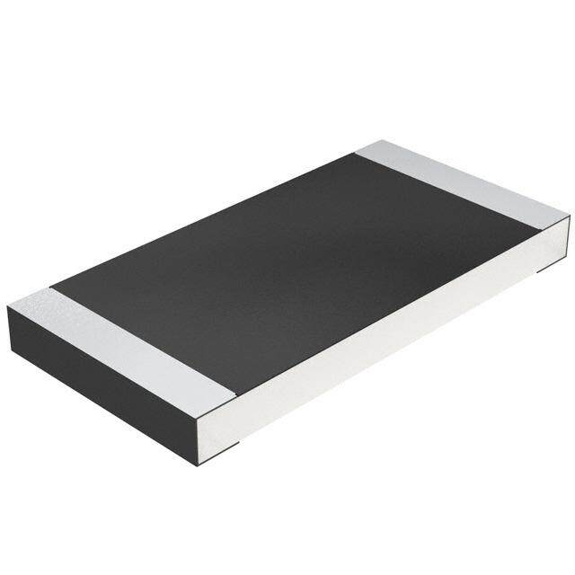
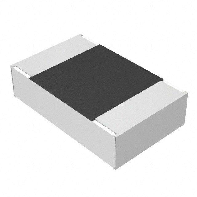
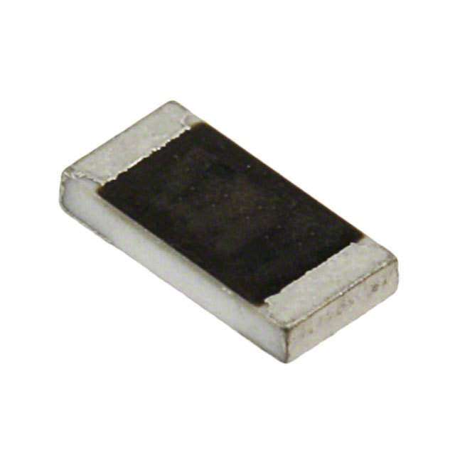
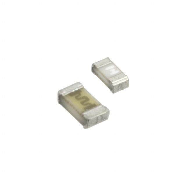
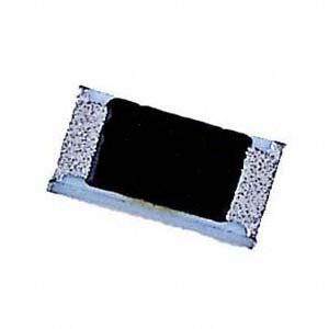
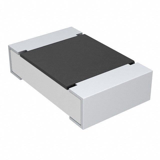
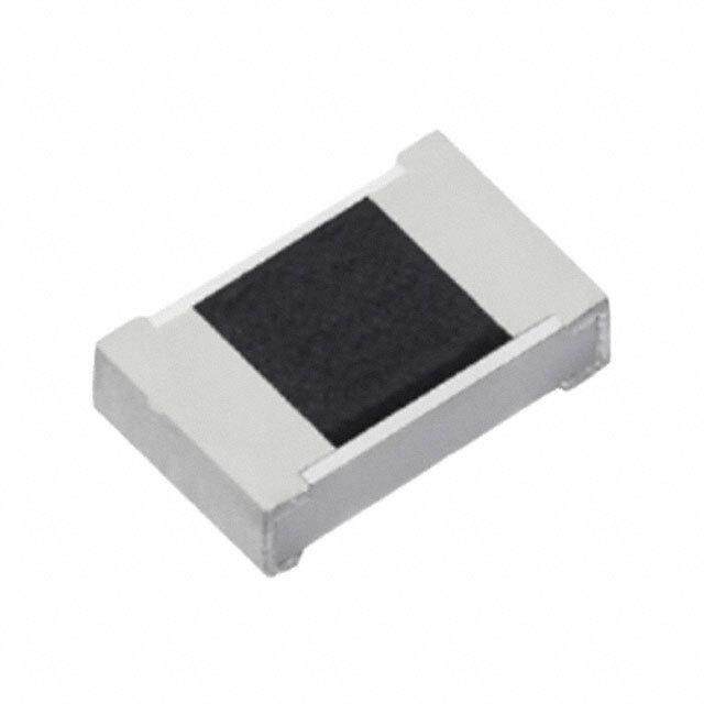
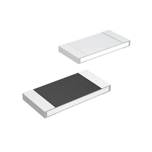
| 产品图片 |
|
| rohs | RoHS 合规性豁免无铅 / 符合限制有害物质指令(RoHS)规范要求 |
| 产品系列 | 薄膜电阻器,厚膜电阻器 - SMD,Vishay / Draloric RCL12251K00JNEGRCL |
| 数据手册 | |
| 产品型号 | RCL12251K00JNEGRCL12251K00JNEG |
| 产品 | Thick Film Resistors SMD |
| 产品种类 | 厚膜电阻器 - SMD |
| 供应商器件封装 | 1225(3263 公制) |
| 其它名称 | RCL1.0KFDKR |
| 功率(W) | 2W |
| 功率额定值 | 2 W |
| 包装 | Digi-Reel® |
| 商标 | Vishay / Draloric |
| 外壳代码-in | 1225 (Reversed) |
| 外壳代码-mm | 3263 (Reversed) |
| 外壳宽度 | 6.3 mm |
| 外壳长度 | 3.2 mm |
| 外壳高度 | 0.75 mm |
| 大小/尺寸 | 0.126" 长 x 0.248" 宽(3.20mm x 6.30mm) |
| 容差 | 5 %±5% |
| 封装 | Reel |
| 封装/外壳 | 宽 2512(6432 公制),1225 |
| 封装/箱体 | 1225 (3263 metric) Reversed |
| 工作温度范围 | - 55 C to + 155 C |
| 成分 | 厚膜 |
| 标准包装 | 10 |
| 温度系数 | ±200ppm/°C200 PPM / K |
| 特性 | 获得 AEC-Q200 汽车认证 |
| 电压额定值 | 200 V |
| 电阻 | 1 kOhms |
| 电阻(Ω) | 1k |
| 端子数 | 2 |
| 类型 | Long Side Termination Thick Film Chip Resistors |
| 系列 | RCL |
| 高度 | 0.035"(0.90mm) |


PDF Datasheet 数据手册内容提取
RCL e3 www.vishay.com Vishay Draloric Long Side Termination Thick Film Chip Resistors FEATURES • Enhanced power rating • Long side terminations • Enhanced thermal cycling performance • Pure tin solder contacts on Ni barrier layer, provides compatibility with lead (Pb)free and lead containing soldering processes • AEC-Q200 qualified • Material categorization: for definitions of compliance RCL e3 resistors series are the perfect choice for most fields please see www.vishay.com/doc?99912 of power measurement electronics where reliability, APPLICATIONS stability, power dissipation, and robust design is of major concern. • Automotive Typical applications include power electronics in automotive • Industrial and industrial appliances. • Commercial TECHNICAL SPECIFICATIONS DESCRIPTION RCL0406 e3 RCL0612 e3 RCL1020 e3 RCL1218 e3 RCL1225 e3 Imperial size 0406 0612 1020 1218 1225 Metric size code RR1016M RR1632M RR2550M RR3246M RR3263M Resistance range 1 Ω to 1 MΩ; jumper (0 Ω) 1 juΩm top e2r. 2(0 M ΩΩ); 1ju Ωm ptoe r1 ( 0M ΩΩ); Resistance tolerance ± 5 %; ± 1 % Temperature coefficient ± 200 ppm/K; ± 100 ppm/K Rated dissipation, P (1) 0.25 W 0.75 W 1.0 W 1.0 W 2.0 W (2) 70 Operating voltage, U AC /DC 50 V 75 V 200 V 200 V 200 V max. RMS Permissible film temperature, ϑ (1) 155 °C F max. Operating temperature range -55 °C to +155 °C Max. resistance change at P 70 for resistance range, |ΔR/R| after: 1000 h ≤ 1.0 % 8000 h ≤ 2.0 % Permissible voltage against ambient (insulation): 1 min, U 100 V 100 V 300 V 300 V 300 V ins Notes (1) Please refer to APPLICATION INFORMATION below (2) Specified power rating requires dedicated mounting conditions to achieve the required thermal resistance APPLICATION INFORMATION When the resistor dissipates power, a temperature rise above the ambient temperature occurs, dependent on the thermal resistance of the assembled resistor together with the printed circuit board. The rated dissipation applies only if the permitted film temperature is not exceeded. These resistors do not feature a limited lifetime when operated within the permissible limits. However, resistance value drift increasing over operating time may result in exceeding a limit acceptable to the specific application, thereby establishing a functional lifetime. Revision: 12-Jul-17 1 Document Number: 20046 For technical questions, contact: thickfilmchip@vishay.com THIS DOCUMENT IS SUBJECT TO CHANGE WITHOUT NOTICE. THE PRODUCTS DESCRIBED HEREIN AND THIS DOCUMENT ARE SUBJECT TO SPECIFIC DISCLAIMERS, SET FORTH AT www.vishay.com/doc?91000
RCL e3 www.vishay.com Vishay Draloric TEMPERATURE COEFFICIENT AND RESISTANCE RANGE TYPE / SIZE TCR TOLERANCE RESISTANCE E-SERIES ± 200 ppm/K ± 5 % 1 Ω to 1 MΩ E24 RCL0406 e3 ± 100 ppm/K ± 1 % 1 Ω to 1 MΩ E24; E96 Jumper, I = 4 A ≤ 10 mΩ 0 Ω - max. ± 200 ppm/K ± 5 % 1 Ω to 1 MΩ E24 RCL0612 e3 ± 100 ppm/K ± 1 % 1 Ω to 1 MΩ E24; E96 Jumper, I = 6 A ≤ 10 mΩ 0 Ω - max. ± 200 ppm/K ± 5 % 1 Ω to 1 MΩ E24 RCL1020 e3 ± 100 ppm/K ± 1 % 1 Ω to 1 MΩ E24; E96 Jumper, I = 10 A ≤ 10 mΩ 0 Ω - max. ± 200 ppm/K ± 5 % 1 Ω to 2.2 MΩ E24 RCL1218 e3 ± 100 ppm/K ± 1 % 1 Ω to 2.2 MΩ E24; E96 Jumper, I = 7 A ≤ 20 mΩ 0 Ω - max. ± 200 ppm/K ± 5 % 1 Ω to 1 MΩ E24 RCL1225 e3 ± 100 ppm/K ± 1 % 1 Ω to 1 MΩ E24; E96 Jumper, I = 12 A ≤ 10 mΩ 0 Ω - max. Note • The temperature coefficient of resistance (TCR) is not specified for 0 Ω jumpers PACKAGING PACKAGING TYPE / SIZE CODE QUANTITY PACKAGING STYLE WIDTH PITCH DIMENSIONS EA = ET1 5000 Ø 180 mm/7" RCL0406 e3 EB = ET5 10 000 4 mm Ø 285 mm/11.25" EC = ET6 20 000 Paper tape acc. to Ø 330 mm/13" 8 mm EA = ET1 5000 IEC 60286-3, Type 1a Ø 180 mm/7" RCL0612 e3 EB = ET5 10 000 4 mm Ø 285 mm/11.25" EC = ET6 20 000 Ø 330 mm/13" RCL1020 e3 EF = E02 4000 4 mm RCL1218 e3 EK = ET9 4000 Blister tape acc. to 12 mm Ø 180 mm/7" EG = E67 2000 IEC 60286-3, Type 2a 8 mm RCL1225 e3 EH = E82 4000 4 mm PART NUMBER AND PRODUCT DESCRIPTION Part Number: RCL061210K0FKEA Part Number: RCL06120000Z0EA R C L 0 6 1 2 1 0 K 0 F K E A MODEL RESISTANCE TOLERANCE TCR PACKAGING RCL0406 R = decimal F = ± 1 % K = ± 100 ppm/K EA RCL0612 K = thousand J = ± 5 % N = ± 200 ppm/K EB RCL1020 M = million Z = jumper 0 = jumper EC RCL1218 0000 = jumper EF RCL1225 EG EH EK Product Description: RCL0612 100 10K 1 % ET1 e3 Product Description: RCL0612 0R0 ET1 e3 RCL0612 100 10K 1 % ET1 e3 MODEL TCR RESISTANCE TOLERANCE PACKAGING LEAD (Pb)-FREE RCL0406 ± 100 ppm/K 10R = 10 Ω ± 1 % ET1 e3 = pure tin RCL0612 ± 200 ppm/K 1K = 1 kΩ ± 5 % ET5 termination RCL1020 10K = 10 kΩ ET6 finish RCL1218 1M0 = 1 MΩ ET9 RCL1225 0R0 = jumper E02 E67 E82 Revision: 12-Jul-17 2 Document Number: 20046 For technical questions, contact: thickfilmchip@vishay.com THIS DOCUMENT IS SUBJECT TO CHANGE WITHOUT NOTICE. THE PRODUCTS DESCRIBED HEREIN AND THIS DOCUMENT ARE SUBJECT TO SPECIFIC DISCLAIMERS, SET FORTH AT www.vishay.com/doc?91000
RCL e3 www.vishay.com Vishay Draloric DESCRIPTION The products do not contain any of the banned substances as per IEC 62474, GADSL, or the SVHC list, Production is strictly controlled and follows an extensive set see www.vishay.com/how/leadfree. of instructions established for reproducibility. A cermet film layer and a glass-over are deposited on a high grade (Al O ) Hence the products fully comply with the following 2 3 ceramic substrate with its prepared inner contacts on both directives: sides. A special laser is used to achieve the target value by • 2000/53/EC End-of-Life Vehicle Directive (ELV) and smoothly fine trimming the resistive layer without damaging Annex II (ELV II) the ceramics. The resistor elements are covered by a • 2011/65/EU Restriction of the Use of Hazardous protective coating designed for electrical, mechanical and Substances Directive (RoHS) with amendment climatic protection. The terminations receive a final pure tin 2015/863/EU on nickel plating. • 2012/19/EU Waste Electrical and Electronic Equipment The result of the determined production is verified by an Directive (WEEE) extensive testing procedure on 100 % of the individual chip Vishay pursues the elimination of conflict minerals from its resistors. Only accepted products are laid directly into the tape in accordance with IEC 60286-3 Type 1a and supply chain, see the Conflict Minerals Policy at Type 2a (1). www.vishay.com/doc?49037. ASSEMBLY APPROVALS The resistors are suitable for processing on automatic SMD The resistors are qualified according to AEC-Q200. assembly systems. They are suitable for automatic Where applicable, the resistors are tested in accordance soldering using wave, reflow or vapor phase as shown in with EN 140401-802 which refers to EN 60115-1, IEC 61760-1 (1). The encapsulation is resistant to all EN 60115-8 and the variety of environmental test cleaning solvents commonly used in the electronics procedures of the IEC 60068 (1) series. industry, including alcohols, esters and aqueous solutions. The suitability of conformal coatings, potting compounds RELATED PRODUCTS and their processes, if applied, shall be qualified by appropriate means to ensure the long-term stability of the The RCA-LS e3, Sulfur Resistant, Long Side Termination whole system. Thick Film Chip Resistors series is designed for harsh environment applications. For ordering RCA-LS e3 products The resistors are RoHS-compliant, the pure tin plating please refer to latest edition of datasheet, provides compatibility with lead (Pb)-free and www.vishay.com/doc?20060. lead-containing soldering processes. Solderability is specified for 2 years after production or requalification. The permitted storage time is 20 years. The immunity of the plating against tin whisker growth has been proven under extensive testing. MATERIALS Vishay acknowledges the following systems for the regulation of hazardous substances: • IEC 62474, Material Declaration for Products of and for the Electrotechnical Industry, with the list of declarable substances given therein (2) • The Global Automotive Declarable Substance List (GADSL) (3) • The REACH regulation (1907/2006/EC) and the related list of substances with very high concern (SVHC) (4) for its supply chain Notes (1) The quoted IEC standards are also released as EN standards with the same number and identical contents (2) The IEC 62474 list of declarable substances is maintained in a dedicated database, which is available at http://std.iec.ch/iec62474 (3) The Global Automotive Declarable Substance List (GADSL) is maintained by the American Chemistry Council and available at www.gadsl.org (4) The SVHC list is maintained by the European Chemical Agency (ECHA) and available at http://echa.europa.eu/candidate-list-table Revision: 12-Jul-17 3 Document Number: 20046 For technical questions, contact: thickfilmchip@vishay.com THIS DOCUMENT IS SUBJECT TO CHANGE WITHOUT NOTICE. THE PRODUCTS DESCRIBED HEREIN AND THIS DOCUMENT ARE SUBJECT TO SPECIFIC DISCLAIMERS, SET FORTH AT www.vishay.com/doc?91000
RCL e3 www.vishay.com Vishay Draloric FUNCTIONAL PERFORMANCE Single Pulse (1) Axis Title 1000 10000 neW) 1225 2 nd lise Load ( 100 1100264011028260 in work ul 1000 P 10 ^P-max. 1 1st line2nd line 100 0.1 0.01 10 0.000001 0.00001 0.0001 0.001 0.01 0.1 1 10 100 t-Pulse Duration (s) i 2nd line Maximum pulse load, single pulse; applicable if P→0 and n < 1000 and Uˆ ≤ Uˆ ; max. for permissible resistance change equivalent to 8000 h operation Continuous Pulse (1) Axis Title neW) 1000 1225 10000 2 nd liLoad ( 100 110260112820 in work se 0406 ul 1000 ntinuous P 101 1st line2nd line o C 100 - max. 0.1 ^P 0.01 10 0.000001 0.00001 0.0001 0.001 0.01 0.1 1 10 100 t-Pulse Duration (s) i 2nd line Maximum pulse load, continuous pulses; applicable if P ≤ P (ϑ ) and Uˆ ≤ Uˆ ; amb max. for permissible resistance change equivalent to 8000 h operation Note (1) Pulse upgrade under review to match upgraded rated dissipation Pulse Voltage Axis Title 800 10000 eV) d linge ( 700 1020,1218, 1225 na 2 Volt 600 ulse 500 1000 ^U-Pmax. 400 1st line2nd line 300 0612 100 200 0406 100 0 10 0.000001 0.00001 0.0001 0.001 0.01 0.1 1 10 t-Pulse Duration (s) i 2nd line Maximum pulse voltage, single and continuous pulses; applicable if Pˆ ≤ Pˆ ; max. for permissible resistance change equivalent to 8000 h operation Revision: 12-Jul-17 4 Document Number: 20046 For technical questions, contact: thickfilmchip@vishay.com THIS DOCUMENT IS SUBJECT TO CHANGE WITHOUT NOTICE. THE PRODUCTS DESCRIBED HEREIN AND THIS DOCUMENT ARE SUBJECT TO SPECIFIC DISCLAIMERS, SET FORTH AT www.vishay.com/doc?91000
RCL e3 www.vishay.com Vishay Draloric Derating Axis Title 70 W) 2.5 10000 n ( RCL1225 o ati 2 ep d linDissi 1000 2n-Power 1.15 RCL1020, RCL1218 1st line2nd line P RCL0612 100 0.5 RCL0406 0 10 -50 0 50 100 150 ϑ -Ambient Temperature (°C) amb 2nd line Revision: 12-Jul-17 5 Document Number: 20046 For technical questions, contact: thickfilmchip@vishay.com THIS DOCUMENT IS SUBJECT TO CHANGE WITHOUT NOTICE. THE PRODUCTS DESCRIBED HEREIN AND THIS DOCUMENT ARE SUBJECT TO SPECIFIC DISCLAIMERS, SET FORTH AT www.vishay.com/doc?91000
RCL e3 www.vishay.com Vishay Draloric TESTS AND REQUIREMENTS All executed tests are carried out in accordance with the The testing also covers most of the requirements specified following specifications: by EIA/IS-703 and JIS-C-5201-1. EN 60115-1, generic specification The tests are carried out under standard atmospheric EN 60115-8 (successor of EN 140400), conditions in accordance with IEC 60068-1, 4.3, whereupon sectional specification the following values are applied: EN 140401-802, detail specification Temperature: 15 °C to 35 °C IEC 60068-2-xx, test methods Relative humidity: 25 % to 75 % The parameters stated in the Test Procedures and Air pressure: 86 kPa to 106 kPa (860 mbar to 1060 mbar). Requirements table are based on the required tests and permitted limits of EN 140401-802. The table presents only the most important tests, for the full test schedule refer to the documents listed above. However, some additional tests and a number of improvements against those minimum requirements have been included. TEST PROCEDURES AND REQUIREMENTS IEC EN 60115-1 60068-2 (1) REQUIREMENTS CLAUSE TEST TEST PROCEDURE PERMISSIBLE CHANGE (ΔR) METHOD STABILITY CLASS 1 STABILITY CLASS 2 Stability for product types: OR BETTER OR BETTER RCL e3 1 Ω to 2.2 MΩ 4.5 - Resistance - ± 1 % ± 5 % Temperature (20 / -55 / 20) °C and 4.8 - ± 100 ppm/K ± 200 ppm/K coefficient (20 / 155 / 20) °C U = P x R or U = U 70 max.; whichever is the less severe; 1.5 h on; 0.5 h off 4.25.1 - Endurance at 70 °C 70 °C; 1000 h ± (1 % R + 0.05 Ω) ± (2 % R + 0.1 Ω) 70 °C; 8000 h ± (2 % R + 0.1 Ω) ± (4 % R + 0.1 Ω) Endurance at 4.25.3 - upper category 155 °C, 1000 h ± (1 % R + 0.05 Ω) ± (2 % R + 0.1 Ω) temperature 4.24 78 (Cab) Damp heat, (40 ± 2) °C; 56 days; ± (1 % R + 0.05 Ω) steady state (93 ± 3) % RH; Damp heat, (85 ± 2) °C; (85 ± 5) % RH; 4.37 67 (Cy) steady state, U = 0.1 x P x R ≤ 100 V; ± (1 % R + 0.05 Ω) ± (2 % R + 0.1 Ω) 70 accelerated 1000 h 4.23 - Climatic sequence: - 4.23.2 2 (Bb) dry heat 125 °C; 16 h 55 °C; 24 h; ≥ 90 % RH; 4.23.3 30 (Db) damp heat, cyclic 1 cycle 4.23.4 1 (Ab) cold -55 °C; 2 h ± (1 % R + 0.05 Ω) ± (2 % R + 0.1 Ω) 4.23.5 13 (M) low air pressure 8.5 kPa; 2 h; (25 ± 10) °C 55 °C; 24 h; 4.23.6 30 (Db) damp heat, cyclic ≥ 90 % RH; 5 cycles 4.23.7 - DC load U = P x R ≤ U 1 min 70 max.; - 1 (Aa) Cold -55 °C; 2 h ± (0.25 % R + 0.05 Ω) ± (0.5 % R + 0.05 Ω) 30 min at -55 °C and 4.19 14 (Na) Rapid change of 30 min at 125 °C; ± (1 % R + 0.05 Ω) temperature 1000 cycles Revision: 12-Jul-17 6 Document Number: 20046 For technical questions, contact: thickfilmchip@vishay.com THIS DOCUMENT IS SUBJECT TO CHANGE WITHOUT NOTICE. THE PRODUCTS DESCRIBED HEREIN AND THIS DOCUMENT ARE SUBJECT TO SPECIFIC DISCLAIMERS, SET FORTH AT www.vishay.com/doc?91000
RCL e3 www.vishay.com Vishay Draloric TEST PROCEDURES AND REQUIREMENTS IEC EN 60115-1 60068-2 (1) REQUIREMENTS CLAUSE TEST TEST PROCEDURE PERMISSIBLE CHANGE (ΔR) METHOD STABILITY CLASS 1 STABILITY CLASS 2 Stability for product types: OR BETTER OR BETTER RCL e3 1 Ω to 2.2 MΩ U = 2.5 x P70 x R ≤ 2 x Umax.; 4.13 - Short time overload whichever is the less severe; ± (2 % R + 0.05 Ω) 5 s Severity no. 4: 4.27 - Single pulse high U = 1U0 =x 2 xP U70 x R or ± (1 % R + 0.05 Ω) voltage overload max.; no visible damage whichever is the less severe; 10 pulses 10 μs/700 μs U = 15 x P x R or 70 Periodic electric U = 2 x Umax.; ± (1 % R + 0.05 Ω) 4.39 - whichever is the less severe; overload no visible damage 0.1 s on; 2.5 s off; 1000 cycles Electrostatic IEC 61340-3-1 (1); 4.38 - discharge 3 pos. + 3 neg. discharges; ± (1 % R + 0.05 Ω) (human body model) ESD voltage acc. to the size Endurance by sweeping; 10 Hz to 2000 Hz; no resonance; ± (0.25 % R + 0.05 Ω) ± (0.5 % R + 0.05 Ω) 4.22 6 (Fc) Vibration amplitude ≤ 1.5 mm or no visible damage no visible damage ≤ 200 m/s2; 7.5 h Solder bath method; Sn60Pb40 non-activated flux; (235 ± 5) °C; (2 ± 0.2) s Good tinning (≥ 95 % covered) 4.17 58 (Td) Solderability Solder bath method; no visible damage Sn96.5Ag3Cu0.5 non-activated flux; (245 ± 5) °C; (3 ± 0.3) s Solder bath method 4.18 58 (Td) Resistance to (260 ± 5) °C; ± (0.25 % R + 0.05 Ω) ± (0.5 % R + 0.05 Ω) soldering heat (10 ± 1) s Component solvent Isopropyl alcohol; 4.29 45 (XA) No visible damage resistance +50 °C; method 2 Shear 4.32 21 (Uu ) 17.7 N No visible damage 3 (adhesion) Depth 2 mm; ± (0.25 % R + 0.05 Ω) 4.33 21 (Uu ) Substrate bending 1 3 times no visible damage, no open circuit in bent position 4.7 - Voltage proof U = 1.4 x U ; 60 s No flashover or breakdown ins Flammability, IEC 60695-11-5 (1); 4.35 - No burning after 30 s needle flame test 10 s Note (1) The quoted IEC standards are also released as EN standards with the same number and identical contents Revision: 12-Jul-17 7 Document Number: 20046 For technical questions, contact: thickfilmchip@vishay.com THIS DOCUMENT IS SUBJECT TO CHANGE WITHOUT NOTICE. THE PRODUCTS DESCRIBED HEREIN AND THIS DOCUMENT ARE SUBJECT TO SPECIFIC DISCLAIMERS, SET FORTH AT www.vishay.com/doc?91000
RCL e3 www.vishay.com Vishay Draloric DIMENSIONS T2 L H W T1 DIMENSIONS AND MASS L W H T1 T2 MASS TYPE / SIZE (mm) (mm) (mm) (mm) (mm) (mg) RCL0406 e3 1.0 ± 0.10 1.6 ± 0.10 0.35 ± 0.10 0.2 +0.10 / -0.15 0.2 ± 0.10 2 RCL0612 e3 1.6 ± 0.20 3.2 ± 0.20 0.55 ± 0.10 0.35 ± 0.15 0.25 ± 0.15 11 RCL1020 e3 2.5 ± 0.20 5.0 ± 0.20 0.55 ± 0.10 0.38 ± 0.15 0.25 ± 0.15 25.5 RCL1218 e3 3.2 +0.10 / -0.20 4.6 ± 0.15 0.55 ± 0.05 0.45 ± 0.20 0.4 ± 0.20 29.5 RCL1225 e3 3.2 ± 0.20 6.3 ± 0.20 0.70 ± 0.10 0.8 ± 0.20 0.4 ± 0.20 55 SOLDER PAD DIMENSIONS G X Y Z RECOMMENDED SOLDER PAD DIMENSIONS WAVE SOLDERING REFLOW SOLDERING TYPE / SIZE G Y X Z G Y X Z (mm) (mm) (mm) (mm) (mm) (mm) (mm) (mm) RCL0406 e3 0.30 0.80 1.95 1.90 0.35 0.60 1.75 1.55 RCL0612 e3 0.50 1.20 3.70 2.90 0.60 1.00 3.50 2.60 RCL1020 e3 1.30 1.25 5.50 3.80 1.30 1.10 5.25 3.50 RCL1218 e3 1.80 1.30 5.10 4.40 1.90 1.10 4.90 4.10 RCL1225 e3 1.10 1.80 6.80 4.70 1.20 1.60 6.60 4.40 Notes • The given solder pad dimensions reflect the considerations for board design and assembly as outlined e.g in standards IEC 61188-5-x (1) or in publication IPC-7351. Still, the given solder pad dimensions will be found adequate for most general applications (1) The quoted IEC standards are also released as EN standards with the same number and identical contents Revision: 12-Jul-17 8 Document Number: 20046 For technical questions, contact: thickfilmchip@vishay.com THIS DOCUMENT IS SUBJECT TO CHANGE WITHOUT NOTICE. THE PRODUCTS DESCRIBED HEREIN AND THIS DOCUMENT ARE SUBJECT TO SPECIFIC DISCLAIMERS, SET FORTH AT www.vishay.com/doc?91000
Legal Disclaimer Notice www.vishay.com Vishay Disclaimer ALL PRODUCT, PRODUCT SPECIFICATIONS AND DATA ARE SUBJECT TO CHANGE WITHOUT NOTICE TO IMPROV E RELIABILITY, FUNCTION OR DESIGN OR OTHERWISE. Vishay Intertechnology, Inc., its affiliates, agents, and employees, and all persons acting on its or their behalf (collectively, “Vishay”), disclaim any and all liability for any errors, inaccuracies or incompleteness contained in any datasheet or in any other disclosure relating to any product. Vishay makes no warranty, representation or guarantee regarding the suitability of the products for any particular purpose o r the continuing production of any product. To the maximum extent permitted by applicable law, Vishay disclaims (i) any and all liability arising out of the application or use of any product, (ii) any and all liability, including without limitation special, consequential or incidental damages, and (iii) any and all implied warranties, including warranties of fitness for particular purpose, non-infringement and merchantability. Statements regarding the suitability of products for certain types of applications are based on Vishay’s knowledge of typical requirements that are often placed on Vishay products in generic applications. Such statements are not binding statements about the suitability of products for a particular application. It is the customer’s responsibility to validate that a particular product with the properties described in the product specification is suitable for use in a particular application. Parameters provided in datasheets and / or specifications may vary in different applications and performance may vary over time. All operating parameters, including typical parameters, must be validated for each customer application by the customer’s technical experts. Product specifications do not expand or otherwise modify Vishay’s terms and conditions of purchase, including but not limited to the warranty expressed therein. Except as expressly indicated in writing, Vishay products are not designed for use in medical, life-saving, or life-sustainin g applications or for any other application in which the failure of the Vishay product could result in personal injury or death. Customers using or selling Vishay products not expressly indicated for use in such applications do so at their own risk . Please contact authorized Vishay personnel to obtain written terms and conditions regarding products designed for such applications. No license, express or implied, by estoppel or otherwise, to any intellectual property rights is granted by this documen t or by any conduct of Vishay. Product names and markings noted herein may be trademarks of their respective owners. © 2019 VISHAY INTERTECHNOLOGY, INC. ALL RIGHTS RESERVED Revision: 01-Jan-2019 1 Document Number: 91000