ICGOO在线商城 > 电阻器 > 芯片电阻 - 表面安装 > RCG040233K0JNED

 Datasheet下载
- 型号: RCG040233K0JNED
- 制造商: Vishay
- 库位|库存: xxxx|xxxx
- 要求:
| 数量阶梯 | 香港交货 | 国内含税 |
| +xxxx | $xxxx | ¥xxxx |
查看当月历史价格
查看今年历史价格
RCG040233K0JNED产品简介:
ICGOO电子元器件商城为您提供RCG040233K0JNED由Vishay设计生产,在icgoo商城现货销售,并且可以通过原厂、代理商等渠道进行代购。 RCG040233K0JNED价格参考。VishayRCG040233K0JNED封装/规格:芯片电阻 - 表面安装, 33 kOhms ±5% 0.063W, 1/16W Chip Resistor 0402 (1005 Metric) Thick Film。您可以下载RCG040233K0JNED参考资料、Datasheet数据手册功能说明书,资料中有RCG040233K0JNED 详细功能的应用电路图电压和使用方法及教程。
Vishay Dale的RCG040233K0JNED是一款0402封装尺寸的精密薄膜表面贴装电阻,阻值为33kΩ,精度±5%(J级),具有优异的稳定性、低温度系数和高可靠性。该型号广泛应用于对空间紧凑性和电气性能要求较高的电子设备中。

主要应用场景包括:便携式医疗设备(如血糖仪、心率监测器)、智能手机与可穿戴设备中的信号调理电路、工业传感器模块、精密测量仪器以及消费类电子产品中的电源管理与反馈控制回路。由于其采用薄膜技术,具备良好的长期稳定性和抗老化性能,适合在环境变化较大的条件下保持精确阻值。

此外,RCG040233K0JNED符合AEC-Q200标准,适用于部分汽车电子系统,如车载传感器、车身控制模块等。其小尺寸设计满足高密度PCB布局需求,适合自动化贴片生产,广泛用于需要微型化与高性能兼顾的现代电子产品中。
| 参数 | 数值 |
| 产品目录 | |
| 描述 | RES 33K OHM 1/16W 5% 0402 SMD厚膜电阻器 - SMD .063watt 33kohms 5% 0402 200ppm |
| 产品分类 | |
| 品牌 | Vishay / DraloricVishay Dale |
| 产品手册 | |
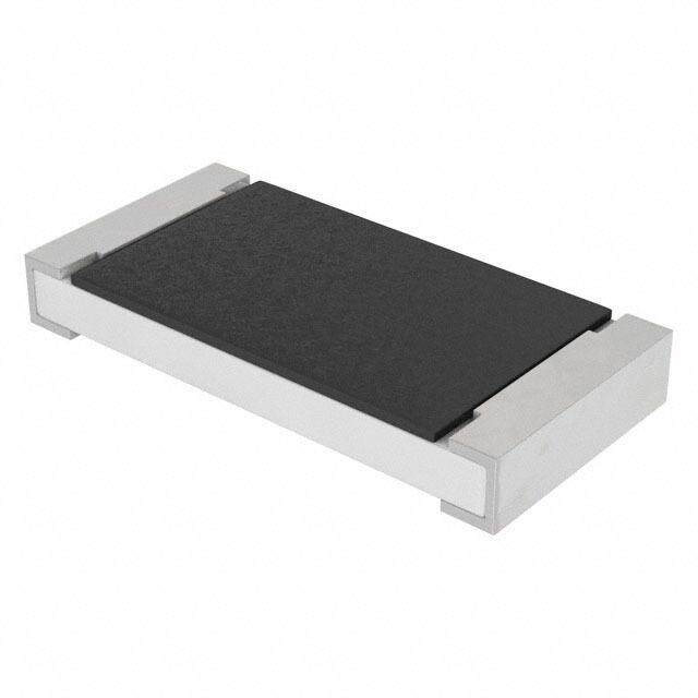
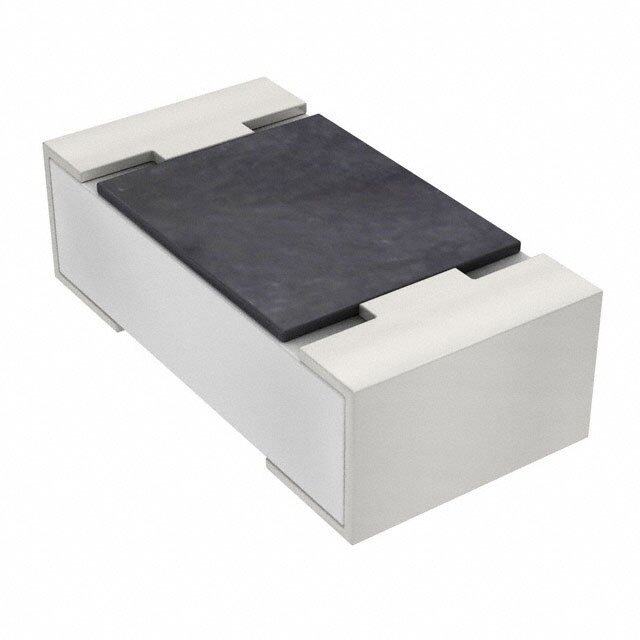
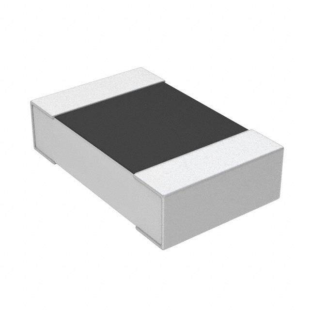
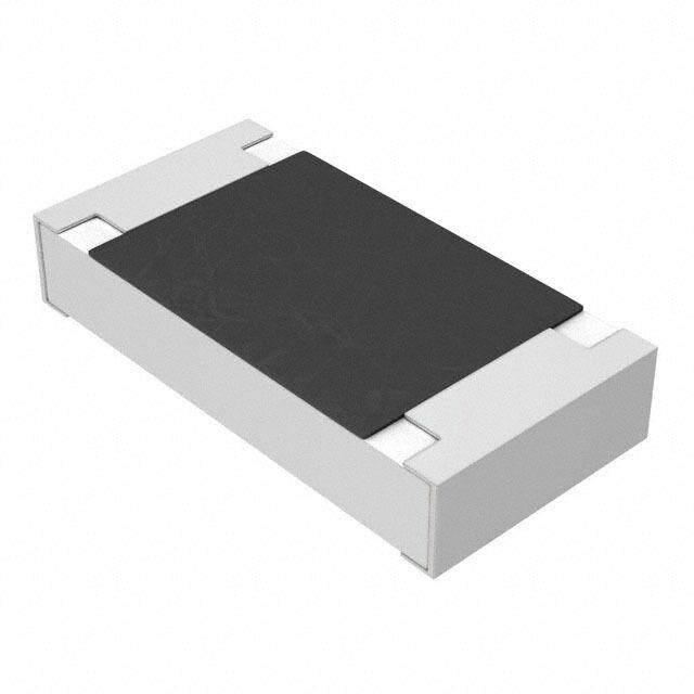
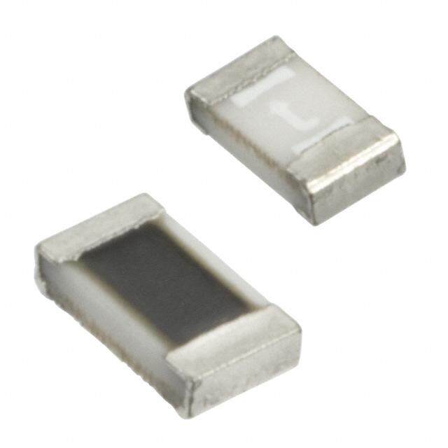
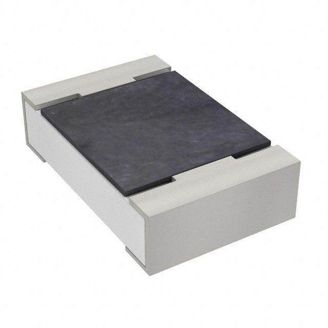
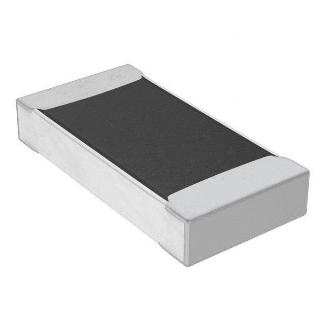
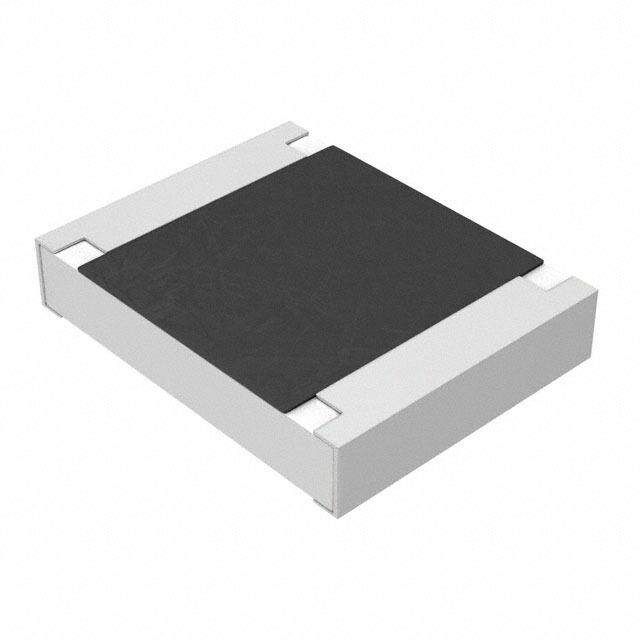
| 产品图片 |
|
| rohs | 符合RoHS无铅 / 符合限制有害物质指令(RoHS)规范要求 |
| 产品系列 | 薄膜电阻器,厚膜电阻器 - SMD,Vishay / Draloric RCG040233K0JNEDRCG |
| 数据手册 | |
| 产品型号 | RCG040233K0JNEDRCG040233K0JNED |
| 产品 | Thick Film Resistors SMD |
| 产品种类 | 厚膜电阻器 - SMD |
| 供应商器件封装 | 0402(1005 公制) |
| 其它名称 | 541-1769-1 |
| 功率(W) | 0.063W,1/16W |
| 功率额定值 | 63 mW |
| 包装 | 剪切带 (CT) |
| 单位重量 | 0.650 mg |
| 商标 | Vishay / Draloric |
| 外壳代码-in | 0402 |
| 外壳代码-mm | 1005 |
| 外壳宽度 | 0.5 mm |
| 外壳长度 | 1 mm |
| 外壳高度 | 0.35 mm |
| 大小/尺寸 | 0.039" 长 x 0.020" 宽(1.00mm x 0.50mm) |
| 容差 | 5 %±5% |
| 封装 | Reel |
| 封装/外壳 | 0402(1005 公制) |
| 封装/箱体 | 0402 (1005 metric) |
| 工作温度范围 | - 55 C to + 155 C |
| 成分 | 厚膜 |
| 标准包装 | 1 |
| 温度系数 | 200 PPM / K±200ppm/°C |
| 特性 | - |
| 特色产品 | http://www.digikey.cn/product-highlights/cn/zh/vishay-rcg-series-thick-film-resistors/3950 |
| 电压额定值 | 50 V |
| 电阻 | 33 kOhms |
| 电阻(Ω) | 33k |
| 端子数 | 2 |
| 系列 | RCG e3 |
| 高度 | 0.016"(0.40mm) |


PDF Datasheet 数据手册内容提取
RCG e3 www.vishay.com Vishay Draloric Green Thick Film Chip Resistors FEATURES • Green resistor - does not use RoHS exemptions • Stability R/R = 1 % for 1000 h at 70 ° C • 2 mm pitch packaging option for 0603 size • Material categorization: for definitions of compliance please see www.vishay.com/doc?99912 STANDARD ELECTRICAL SPECIFICATIONS LIMITING ELEMENT CASE CASE POWER RATING TEMPERATURE RESISTANCE VOLTAGE TOLERANCE TYPE SIZE SIZE P COEFFICIENT RANGE SERIES 70 U ± % IMPERIAL METRIC W max. ± ppm/K AC /DC RMS V 100 150 to 10M 0.5, 1 E24; E96 0.063 50 150 1.0 to 147 RCG0402 0402 RR1005M 200 5 1.0 to 10M E24 Zero-Ohm-Resistor: Rmax. = 20 m, Imax. = 1.5 A 100 0.5, 1 E24; E96 0.1 75 1.0 to 10M RCG0603 0603 RR1608M 200 5 E24 Zero-Ohm-Resistor: Rmax. = 20 m, Imax. = 2.0 A 100 0.5, 1 E24; E96 0.125 150 1.0 to 10M RCG0805 0805 RR2012M 200 5 E24 Zero-Ohm-Resistor: Rmax. = 20 m, Imax. = 2.5 A 100 0.5, 1 E24; E96 0.25 200 1.0 to 10M RCG1206 1206 RR3216M 200 5 E24 Zero-Ohm-Resistor: Rmax. = 20 m, Imax. = 3.5 A Notes • These resistors do not feature a limited lifetime when operated within the permissible limits. However, resistance value drift increasing over operating time may result in exceeding a limit acceptable to the specific application, thereby establishing a functional lifetime. • Marking: See datasheet “Surface Mount Resistor Marking” (document number 20020). • Power rating depends on the max. temperature at the solder point, the component placement density and the substrate material. TECHNICAL SPECIFICATIONS PARAMETER UNIT RCG0402 RCG0603 RCG0805 RCG1206 Rated dissipation P (1) W 0.063 0.1 0.125 0.25 70 Operating voltage U AC /DC V 50 75 150 200 max. RMS Insulation voltage U (1 min) V 75 100 200 300 ins Insulation resistance > 109 Operating temperature range °C - 55 to + 155 Mass mg 0.65 2 5.5 10 Note (1) The power dissipation on the resistor generates a temperature rise against the local ambient, depending on the heat flow support of the printed-circuit board (thermal resistance). The rated dissipation applies only if the permitted film temperature of 155 °C is not exceeded. Revision: 01-Sep-14 1 Document Number: 20047 For technical questions, contact: thickfilmchip@vishay.com THIS DOCUMENT IS SUBJECT TO CHANGE WITHOUT NOTICE. THE PRODUCTS DESCRIBED HEREIN AND THIS DOCUMENT ARE SUBJECT TO SPECIFIC DISCLAIMERS, SET FORTH AT www.vishay.com/doc?91000
RCG e3 www.vishay.com Vishay Draloric PART NUMBER AND PRODUCT DESCRIPTION PART NUMBER: RCG080510K0FKEA R C G 0 8 0 5 1 0 K 0 F K E A TYPE VALUE TOLERANCE TCR PACKAGING RCG0402 R = Decimal D = ± 0.5 % K = ± 100 ppm/K EA, EB, RCG0603 K = Thousand F = ± 1.0 % L = ± 150 ppm/K EC, ED, RCG0805 M = Million J = ± 5.0 % N = ± 200 ppm/K EE, EI, RCG1206 0000 = 0 Jumper Z = Jumper 0 = Jumper EL PRODUCT DESCRIPTION: RCG0805 100 10K 1 % EA RCG0805 100 10K 1 % EA TYPE TCR RESISTANCE VALUE TOLERANCE PACKAGING RCG0402 ± 100 ppm/K 10R = 10 ± 0.5 % EA, EB, RCG0603 ± 150 ppm/K 10K = 10 k ± 1 % EC, ED, RCG0805 ± 200 ppm/K 1M = 1 M ± 5 % EE, EI, RCG1206 0R0 = Jumper EL PACKAGING TYPE CODE QUANTITY CARRIER TAPE WIDTH PITCH REEL DIAMETER ED 10 000 Paper tape acc. 180 mm/7" RCG0402 to IEC 60286-3 8 mm 2 mm EE 50 000 Type 1a 330 mm/13" EI 5000 180 mm/7" ED 10 000 Paper tape acc. 180 mm/7" to IEC 60268-3 8 mm 2 mm EL 20 000 Type 1a 285 mm/11.25" RCG0603 EE 50 000 330 mm/13" EA 5000 180 mm/7" Paper tape acc. EB 10 000 to IEC 60268-3 8 mm 4 mm 285 mm/11.25" Type 1a EC 20 000 330 mm/13" EA 5000 180 mm/7" Paper tape acc. RCG0805 EB 10 000 to IEC 60268-3 8 mm 4 mm 285 mm/11.25" Type 1a EC 20 000 330 mm/13" EA 5000 180 mm/7" Paper tape acc. RCG1206 EB 10 000 to IEC 60268-3 8 mm 4 mm 285 mm/11.25" Type 1a EC 20 000 330 mm/13" Revision: 01-Sep-14 2 Document Number: 20047 For technical questions, contact: thickfilmchip@vishay.com THIS DOCUMENT IS SUBJECT TO CHANGE WITHOUT NOTICE. THE PRODUCTS DESCRIBED HEREIN AND THIS DOCUMENT ARE SUBJECT TO SPECIFIC DISCLAIMERS, SET FORTH AT www.vishay.com/doc?91000
RCG e3 www.vishay.com Vishay Draloric DIMENSIONS in millimeters SOLDER PAD DIMENSIONS SIZE DIMENSIONS REFLOW SOLDERING WAVE SOLDERING IMPERIAL METRIC L W H T1 T2 a b l a b l 0402 RR1005M 1.0 ± 0.05 0.5 ± 0.05 0.35 ± 0.05 0.25 ± 0.05 0.2 ± 0.1 0.4 0.6 0.5 0603 RR1608M 1.55 + 0.10 0.85 ± 0.1 0.45 ± 0.05 0.3 ± 0.2 0.3 ± 0.2 0.5 0.9 1.0 0.9 0.9 1.0 - 0.05 0805 RR2012M 2.0 + 0.20 1.25 ± 0.15 0.45 ± 0.05 0.3+ 0.20 0.3 ± 0.2 0.7 1.3 1.2 0.9 1.3 1.3 - 0.10 - 0.10 1206 RR3216M 3.2 + 0.10 1.6 ± 0.15 0.55 ± 0.05 0.45 ± 0.2 0.4 ± 0.2 0.9 1.7 2.0 1.1 1.7 2.3 - 0.20 FUNCTIONAL PERFORMANCE P70 n atio 100 p ssi % Di d e at R of n 50 o cti a Fr 0 - 50 0 50 70 100 °C 150 Derating Ambient Temperature in amb GREEN REQUIREMENTS SUBSTANCES CONCENTRATION LIMIT Lead (Pb) < 1000 ppm Mercury (Hg) < 1000 ppm Cadmium (Cd) < 100 ppm Hexavalent Chronium < 1000 ppm Polybrominated Biphenyl (PBB) < 1000 ppm Polybrominated Diphenyl Ether (PBDE) < 1000 ppm Bromine (Br) < 900 ppm Chlorine (Cl) < 900 ppm Sum of Bromine and Chlorine 1500 ppm max. Antimony (Sb) < 900 ppm Red Phosphorous < 100 ppm Notes • No exemptions (e.g. Pb in glass) may be applied to any substances or application for the “Green” category • All concentration levels are based on homogenous materials Revision: 01-Sep-14 3 Document Number: 20047 For technical questions, contact: thickfilmchip@vishay.com THIS DOCUMENT IS SUBJECT TO CHANGE WITHOUT NOTICE. THE PRODUCTS DESCRIBED HEREIN AND THIS DOCUMENT ARE SUBJECT TO SPECIFIC DISCLAIMERS, SET FORTH AT www.vishay.com/doc?91000
RCG e3 www.vishay.com Vishay Draloric TEST PROCEDURES AND REQUIREMENTS IEC EN 60115-1 60068-2 REQUIREMENTS TEST PROCEDURE CLAUSE TEST PERMISSIBLE CHANGE (R) METHOD STABILITY CLASS 1 STABILITY CLASS 2 Stability for product types: OR BETTER OR BETTER RCG e3 1 to 10 M 1 to 10 M 4.5 - Resistance - ± 0.5 %, ± 1 % ± 5 % 4.7 - Voltage proof U = 1.4 x U ; 60 s No flashover or breakdown ins 4.13 - Short time overload U = 2.5 x P70 x R 2 x Umax.; ± (0.25 % R + 0.05 ) ± (0.5 % R + 0.05 ) Duration acc. to style Solder bath method; Sn96.5Ag3Cu0.5 Good tinning ( 95 % covered) 4.17.2 58 (Td) Solderability non-activated flux; no visible damage (245 ± 5) °C (3 ± 0.3) s Temperature (20/- 55/20) °C and 4.8.4.2 - ± 100 ppm/K, ± 150 ppm/K ± 200 ppm/K coefficient (20/125/20) °C Shear RR 1608 and smaller: 9 N 4.32 21 (Uu ) No visible damage 3 (adhesion) RR 2012 and larger: 45 N No visible damage, no open circuit in bent position Depth 2 mm; 4.33 21 (Uu ) Substrate bending 1 3 times ± (0.25 % R + 0.05 ) ± (0.5 % R + 0.05 ) 4.23 - Climatic sequence: - 4.23.2 2 (Ba) Dry heat 125 °C; 16 h 55 °C; 90 % RH; 4.23.3 30 (Db) Damp heat, cyclic 24 h; 1 cycle 4.23.4 1 (Aa) Cold - 55 °C; 2 h ± (1 % R + 0.05 ) ± (2 % R + 0.1 ) 4.23.5 13 (M) Low air pressure 1 kPa; (25 ± 10) °C; 1 h 55 °C; 90 % RH; 4.23.6 30 (Db) Damp heat, cyclic 24 h; 5 cycles 4.23.7 - DC load U = P x R 70 U = P70 x R Umax.; 1.5 h on; 0.5 h off; 4.25.1 - Endurance at 70 °C 70 °C; 1000 h ± (1 % R + 0.05 ) ± (2 % R + 0.1 ) Solder bath method Resistance to 4.18.2 58 (Td) (260 ± 5) °C; ± (0.25 % R + 0.05 ) ± (0.5 % R + 0.05 ) soldering heat (10 ± 1) s Flamability, IEC 60695-11-5; 4.35 - No burning after 30 s needle flame test 10 s (40 ± 2) °C; Damp heat, 4.24 78 (Cab) (93 ± 3) % RH; ± (1 % R + 0.05 ) ± (1 % R + 0.1 ) steady state 56 days Endurance at 4.25.3 - upper category 155 °C, 1000 h ± (1 % R + 0.05 ) ± (2 % R + 0.1 ) temperature Electrostatic IEC 61340-3-1; 4.40 - discharge 3 pos. + 3 neg. discharges; ± (1 % R + 0.05 ) (human body model) ESD test voltage acc. to size Revision: 01-Sep-14 4 Document Number: 20047 For technical questions, contact: thickfilmchip@vishay.com THIS DOCUMENT IS SUBJECT TO CHANGE WITHOUT NOTICE. THE PRODUCTS DESCRIBED HEREIN AND THIS DOCUMENT ARE SUBJECT TO SPECIFIC DISCLAIMERS, SET FORTH AT www.vishay.com/doc?91000
RCG e3 www.vishay.com Vishay Draloric TEST PROCEDURES AND REQUIREMENTS IEC EN 60115-1 60068-2 REQUIREMENTS TEST PROCEDURE CLAUSE TEST PERMISSIBLE CHANGE (R) METHOD STABILITY CLASS 1 STABILITY CLASS 2 Stability for product types: OR BETTER OR BETTER RCG e3 1 to 10 M 1 to 10 M Component solvent Isopropyl alcohol; 4.29 45 (XA) No visible damage resistance 50 °C; method 2 Isopropyl alcohol; Solvent resistance Marking legible, 4.30 45 (XA) 50 °C; method 1, of marking no visible damage toothbrush f = 10 Hz to 2000 Hz; Vibration, endurance x, y, z 1.5 mm; 4.22 6 (Fc) ± (0.25 % R + 0.05 ) ± (0.5 % R + 0.05 ) by sweeping A 200 m/s2; 10 sweeps per axis U = 15 x P x R 70 4.37 - Periodic electric 2 x Umax.; ± (1 % R + 0.05 ) overload 0.1 s on; 2.5 s off; 1000 cycles Single pulse high Û = 10 x P x R 70 4.27 - voltage overload, 2 x Umax.; ± (1 % R + 0.05 ) 10 μs/700 μs 10 pulses All tests are carried out in accordance with the following specifications: • EN 60115-1, generic specification • EN 140400, sectional specification • EN 140401-802, detail specification • IEC 60068-2, environmental test procedures Packaging of components is done in paper tapes according to IEC 60286-3. Revision: 01-Sep-14 5 Document Number: 20047 For technical questions, contact: thickfilmchip@vishay.com THIS DOCUMENT IS SUBJECT TO CHANGE WITHOUT NOTICE. THE PRODUCTS DESCRIBED HEREIN AND THIS DOCUMENT ARE SUBJECT TO SPECIFIC DISCLAIMERS, SET FORTH AT www.vishay.com/doc?91000
Legal Disclaimer Notice www.vishay.com Vishay Disclaimer ALL PRODUCT, PRODUCT SPECIFICATIONS AND DATA ARE SUBJECT TO CHANGE WITHOUT NOTICE TO IMPROV E RELIABILITY, FUNCTION OR DESIGN OR OTHERWISE. Vishay Intertechnology, Inc., its affiliates, agents, and employees, and all persons acting on its or their behalf (collectively, “Vishay”), disclaim any and all liability for any errors, inaccuracies or incompleteness contained in any datasheet or in any other disclosure relating to any product. Vishay makes no warranty, representation or guarantee regarding the suitability of the products for any particular purpose o r the continuing production of any product. To the maximum extent permitted by applicable law, Vishay disclaims (i) any and all liability arising out of the application or use of any product, (ii) any and all liability, including without limitation special, consequential or incidental damages, and (iii) any and all implied warranties, including warranties of fitness for particular purpose, non-infringement and merchantability. Statements regarding the suitability of products for certain types of applications are based on Vishay’s knowledge of typical requirements that are often placed on Vishay products in generic applications. Such statements are not binding statements about the suitability of products for a particular application. It is the customer’s responsibility to validate that a particular product with the properties described in the product specification is suitable for use in a particular application. Parameters provided in datasheets and / or specifications may vary in different applications and performance may vary over time. All operating parameters, including typical parameters, must be validated for each customer application by the customer’s technical experts. Product specifications do not expand or otherwise modify Vishay’s terms and conditions of purchase, including but not limited to the warranty expressed therein. Except as expressly indicated in writing, Vishay products are not designed for use in medical, life-saving, or life-sustainin g applications or for any other application in which the failure of the Vishay product could result in personal injury or death. Customers using or selling Vishay products not expressly indicated for use in such applications do so at their own risk . Please contact authorized Vishay personnel to obtain written terms and conditions regarding products designed for such applications. No license, express or implied, by estoppel or otherwise, to any intellectual property rights is granted by this documen t or by any conduct of Vishay. Product names and markings noted herein may be trademarks of their respective owners. © 2019 VISHAY INTERTECHNOLOGY, INC. ALL RIGHTS RESERVED Revision: 01-Jan-2019 1 Document Number: 91000