ICGOO在线商城 > PYB15-Q48-D5-DIN
 Datasheet下载
- 型号: PYB15-Q48-D5-DIN
- 制造商: CUI/STACK INCORPORATED
- 库位|库存: xxxx|xxxx
- 要求:
| 数量阶梯 | 香港交货 | 国内含税 |
| +xxxx | $xxxx | ¥xxxx |
查看当月历史价格
查看今年历史价格
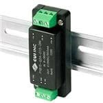
PYB15-Q48-D5-DIN产品简介:
ICGOO电子元器件商城为您提供PYB15-Q48-D5-DIN由CUI/STACK INCORPORATED设计生产,在icgoo商城现货销售,并且可以通过原厂、代理商等渠道进行代购。 提供PYB15-Q48-D5-DIN价格参考¥266.86-¥282.63以及CUI/STACK INCORPORATEDPYB15-Q48-D5-DIN封装/规格参数等产品信息。 你可以下载PYB15-Q48-D5-DIN参考资料、Datasheet数据手册功能说明书, 资料中有PYB15-Q48-D5-DIN详细功能的应用电路图电压和使用方法及教程。
| 参数 | 数值 |
| 产品目录 | |
| 描述 | DC/DC CONVERTER +/-5V 15W DIN |
| 产品分类 | DC DC Converters |
| 品牌 | CUI Inc |
| 数据手册 | |
| 产品图片 |
|
| 产品型号 | PYB15-Q48-D5-DIN |
| rohs | 无铅 / 符合限制有害物质指令(RoHS)规范要求 |
| RoHS指令信息 | http://www.cui.com/product/resource/digikeyrohs/pyb15-din-series |
| 产品系列 | PYB15-DIN |
| 不同电流时的输出(最大值)-1 | 5 VDC @ 1.5A |
| 不同电流时的输出(最大值)-2 | -5 VDC @ 1.5A |
| 不同电流时的输出(最大值)-3 | - |
| 不同电流时的输出(最大值)-4 | - |
| 产品培训模块 | http://www.digikey.cn/PTM/IndividualPTM.page?site=cn&lang=zhs&ptm=30387http://www.digikey.cn/PTM/IndividualPTM.page?site=cn&lang=zhs&ptm=30568 |
| 其它名称 | 102-3174 |
| 功率(W) | 15W |
| 功率(W)-最大值 | 15W |
| 包装 | 散装 |
| 大小/尺寸 | 2.99" 长 x 1.24" 宽 x 0.87" 高 (76.0mm x 31.5mm x 22.2mm) |
| 安装类型 | DIN 轨道 |
| 封装/外壳 | 模块 |
| 工作温度 | -40°C ~ 85°C |
| 效率 | 84% |
| 标准包装 | 40 |
| 特色产品 | http://www.digikey.cn/product-highlights/cn/zh/cui-pyb-series-converters/3947http://www.digikey.cn/product-highlights/zh/din-rail-dcdc-converters/52376 |
| 电压-输入 | 18 ~ 75 V |
| 相关产品 | /product-detail/zh/AT8-DLA1/255-1210-ND/252287/product-detail/zh/TS3575SL/ADR3575-S7874-ND/382570/product-detail/zh/TS3575SOL/ADR3575-U7874-ND/382647/product-detail/zh/TS3515SL/ADR3515-S7874-ND/382724/product-detail/zh/TS3515SOL/ADR3515-U7874-ND/382801/product-detail/zh/NDNA200/NDNA200-ND/2173971/product-detail/zh/NDNA100/283-3994-ND/2173974/product-detail/zh/NDNA8/NDNA8-ND/2173975/product-detail/zh/ATBDR351/ATBDR351-ND/2413920/product-detail/zh/ATBDR35151/ATBDR35151-ND/2413921/product-detail/zh/ATBDR35152/ATBDR35152-ND/2413922/product-detail/zh/ATBDR3515S1/ATBDR3515S1-ND/2413923/product-detail/zh/ATBDR3515S2/ATBDR3515S2-ND/2413924/product-detail/zh/ATBDR352/ATBDR352-ND/2413925/product-detail/zh/ATBDR35S1/ATBDR35S1-ND/2413926/product-detail/zh/ATBDR35S2/ATBDR35S2-ND/2413927/product-detail/zh/DNR-4790/377-1952-ND/3313448 |
| 类型 | 隔离 |
| 认可 | EN,IEC |
| 输出 | ±5V |
| 输出数 | 2 |

.jpg)


- 商务部:美国ITC正式对集成电路等产品启动337调查
- 曝三星4nm工艺存在良率问题 高通将骁龙8 Gen1或转产台积电
- 太阳诱电将投资9.5亿元在常州建新厂生产MLCC 预计2023年完工
- 英特尔发布欧洲新工厂建设计划 深化IDM 2.0 战略
- 台积电先进制程称霸业界 有大客户加持明年业绩稳了
- 达到5530亿美元!SIA预计今年全球半导体销售额将创下新高
- 英特尔拟将自动驾驶子公司Mobileye上市 估值或超500亿美元
- 三星加码芯片和SET,合并消费电子和移动部门,撤换高东真等 CEO
- 三星电子宣布重大人事变动 还合并消费电子和移动部门
- 海关总署:前11个月进口集成电路产品价值2.52万亿元 增长14.8%


PDF Datasheet 数据手册内容提取
Additional Resources: Product Page | 3D Model ddaattee 06/21/2019 ppaaggee 11 ooff 77 SERIES: PYB15-DIN │ DESCRIPTION: DC-DC CONVERTER FEATURES • up to 15 W isolated output • industry standard pinout • 4:1 input range (9~36 Vdc, 18~75 Vdc) • smaller package • single/dual regulated outputs • 1,500 Vdc isolation • continuous short circuit, over current protection, over voltage protection • reverse polarity protection • temperature range (-40~85°C) • six-sided metal shielding • efficiency up to 88% MODEL input output output output ripple efficiency voltage voltage current power and noise1 typ range min max max max typ (Vdc) (Vdc) (Vdc) (mA) (mA) (W) (mVp-p) (%) PYB15-Q24-S3-DIN 24 9~36 3.3 200 4000 13.2 100 85 PYB15-Q24-S5-DIN 24 9~36 5 150 3000 15 100 88 PYB15-Q24-S12-DIN 24 9~36 12 63 1250 15 100 87 PYB15-Q24-S15-DIN 24 9~36 15 50 1000 15 100 87 PYB15-Q24-S24-DIN 24 9~36 24 31 625 15 100 88 PYB15-Q24-D5-DIN 24 9~36 ±5 ±75 ±1500 15 100 84 PYB15-Q24-D12-DIN 24 9~36 ±12 ±32 ±625 15 100 86 PYB15-Q24-D15-DIN 24 9~36 ±15 ±25 ±500 15 100 86 PYB15-Q48-S3-DIN 48 18~75 3.3 200 4000 13.2 100 85 PYB15-Q48-S5-DIN 48 18~75 5 150 3000 15 100 87 PYB15-Q48-S12-DIN 48 18~75 12 63 1250 15 100 86 PYB15-Q48-S15-DIN 48 18~75 15 50 1000 15 100 88 PYB15-Q48-D5-DIN 48 18~75 ±5 ±75 ±1500 15 100 84 PYB15-Q48-D12-DIN 48 18~75 ±12 ±32 ±625 15 100 86 PYB15-Q48-D15-DIN 48 18~75 ±15 ±25 ±500 15 100 87 Notes: 1. Ripple and noise are measured at 20 MHz BW by “parallel cable” method with 1 µF ceramic and 10 µF electrolytic capacitors on the output. PART NUMBER KEY PYB15 - QXX - XXX - X - DIN Mounting Type Base Number DIN = DIN-rail mount Input Voltage Output Heatsink* S = single Output Voltage "blank" = no heatsink D = dual H = with heatsink Notes: *Discontinued heatsink versions. cui.com
Additional Resources: Product Page | 3D Model CUI Inc │ SERIES: PYB15-DIN │ DESCRIPTION: DC-DC CONVERTER date 06/21/2019 │ page 2 of 7 INPUT parameter conditions/description min typ max units 24 Vdc input models 9 24 36 Vdc operating input voltage 48 Vdc input models 18 48 75 Vdc 24 Vdc input models 9 Vdc start-up voltage 48 Vdc input models 17.8 Vdc 24 Vdc input models 7.5 Vdc under voltage shutdown1 48 Vdc input models 16 Vdc for maximum of 1 second surge voltage 24 Vdc input models -0.7 50 Vdc 48 Vdc input models -0.7 100 Vdc start-up time nominal input, constant load 10 ms filter pi filter models ON (CTRL open or connect TTL high level, 2.5~12 Vdc) CTRL2 models OFF (CTRL connect GND or low level, 0~1.2 Vdc) input current (models OFF) 1 mA Notes: 1. Contact CUI if you are planning to use this feature in your application. 2. CTRL pin voltage is referenced to GND. OUTPUT parameter conditions/description min typ max units line regulation full load, input voltage from low to high ±0.2 ±0.5 % load regulation 5% to 100% load ±0.5 ±1 % dual output models: cross regulation main output 50% load, secondary output from ±5 % 10% to 100% load voltage accuracy ±1 ±3 % voltage balance3 dual output, balanced loads ±0.5 ±1 % adjustability4 ±10 % switching frequency PWM mode 300 kHz transient recovery time 25% load step change 300 500 μs transient response deviation 25% load step change ±3 ±5 % temperature coefficient 100% load ±0.02 %/°C Note: 3. For dual output models, unbalanced loads should not exceed ±5%. If ±5% is exceeded, it may not meet all specifications. 4. Output trimming available on single output models only. PROTECTIONS parameter conditions/description min typ max units short circuit protection hiccup, continuous, automatic recovery over current protection 160 % 3.3 Vdc output models 3.9 Vdc 5 Vdc output models 6.2 Vdc over voltage protection 12 Vdc output models 15 Vdc 15 Vdc output models 18 Vdc 24 Vdc output models 30 Vdc SAFETY AND COMPLIANCE parameter conditions/description min typ max units isolation voltage input to output for 1 minute at 1 mA max. 1,500 Vdc isolation resistance input to output at 500 Vdc 1,000 MΩ cui.com
Additional Resources: Product Page | 3D Model CUI Inc │ SERIES: PYB15-DIN │ DESCRIPTION: DC-DC CONVERTER date 06/21/2019 │ page 3 of 7 SAFETY AND COMPLIANCE (CONTINUED) parameter conditions/description min typ max units conducted emissions CISPR22/EN55022, class A, class B (external circuit required, see Figure 1-b) radiated emissions CISPR22/EN55022, class A, class B (external circuit required, see Figure 1-b) ESD IEC/EN61000-4-2, class B, contact ± 4kV radiated immunity IEC/EN61000-4-3, class A, 10V/m EFT/burst IEC/EN61000-4-4, class B, ± 2kV (external circuit required, see Figure 1-a) surge IEC/EN61000-4-5, class B, ± 2kV (external circuit required, see Figure 1-a) conducted immunity IEC/EN61000-4-6, class A, 3 Vr.m.s voltage dips & interruptions IEC/EN61000-4-29, class B, 0%-70% MTBF as per MIL-HDBK-217F @ 25°C 1,000,000 hours RoHS 2011/65/EU ENVIRONMENTAL parameter conditions/description min typ max units operating temperature see derating curves -40 85 °C storage temperature -55 125 °C storage humidity non-condensing 5 95 % case temperature at full load, Ta=71°C 105 °C vibration 10~55 Hz for 30 min. along X, Y and Z axis 10 G MECHANICAL parameter conditions/description min typ max units DIN-rail mount: 76 x 31.5 x 25.8 mm dimensions DIN-rail mount with heatsink: 76 x 31.5 x 29.7 mm case material aluminum alloy DIN-rail mount 70 g weight DIN-rail mount with heatsink 78 g cui.com
Additional Resources: Product Page | 3D Model CUI Inc │ SERIES: PYB15-DIN │ DESCRIPTION: DC-DC CONVERTER date 06/21/2019 │ page 4 of 7 MECHANICAL DRAWING DIN-RAIL MOUNT units: mm[inch] tolerance: ±0.50[±0.02] wire range: 24~12 AWG mounts to TS35 rails PIN CONNECTIONS Single Dual PIN Output Output 1 CTRL CTRL 2 GND GND Top View 3 Vin Vin 4 0V -Vo 5 Trim 0V 6 +Vo +Vo Front View DIN-RAIL MOUNT WITH HEATSINK units: mm[inch] tolerance: ±0.50[±0.02] wire range: 24~12 AWG mounts to TS35 rails PIN CONNECTIONS Single Dual PIN Output Output 1 CTRL CTRL 2 GND GND 3 Vin Vin Top View 4 0V -Vo 5 Trim 0V 6 +Vo +Vo Front View cui.com
Additional Resources: Product Page | 3D Model CUI Inc │ SERIES: PYB15-DIN │ DESCRIPTION: DC-DC CONVERTER date 06/21/2019 │ page 5 of 7 DERATING CURVES With heatsink 100 80 ) % Without heatsink ( 60 d a o Safe operating area L 40 20 -40 -20 0 20 40 6065 85 Ambient Temperature (°C) EMC RECOMMENDED CIRCUIT Table 1 Figure 1 Recommended external circuit components Vin (Vdc) 24 48 FUSE LDM1 CY1 Vin Vin +Vo FUSE Choose according to input current MOV S14K35 S14K60 + MOV C0 C1 DC/DC Cout LOAD LDM1 4.7μH 4.7μH GND GND -Vo C0 330μF/50V 330μF/100V (a) (b) (0V) CY2 C1 1μF/50V 1μF/100V CY1 1nF/2kV 1nF/2kV CY2 1nF/2kV 1nF/2kV Note: 1. See Table 2 for Cout values. cui.com
Additional Resources: Product Page | 3D Model CUI Inc │ SERIES: PYB15-DIN │ DESCRIPTION: DC-DC CONVERTER date 06/21/2019 │ page 6 of 7 APPLICATION NOTES 1. Recommended circuit This series has been tested according to the following recommended testing circuit before leaving the factory. This series should be tested under load (see Figure 2). If you want to further decrease the input/output ripple, you can increase the capacitance accord- ingly or choose capacitors with low ESR (see Table 2). However, the capacitance of the output filter capacitor must be appropriate. If the capacitance is too high, a startup problem might arise. For every channel of the output, to ensure safe and reliable operation, the maximum capacitance must be less than the maximum capacitive load (see Table 3). Figure 2 Single Output Dual Output +Vo Vin +Vo Vin Cout Cin DC DC Cout Cin DC DC 0V Cout GND 0V GND -Vo Table 2 Table 3 Sing le Vout Cin Cout Dual Vout Cin Cout1 Single Vout Max. Capacitive Load Dual Vout Max. Capacitive Load1 ( Vdc) (µF) (µF) (Vdc) (µF) (µF) (Vdc) (μF) (Vdc) (μF) 3.3 100 470 -- -- -- 3.3 10200 -- -- 5 100 470 ±5 100 220 5 4020 5 4800 12 100 220 ±12 100 100 12 1035 12 800 15 100 220 ±15 100 100 15 705 15 500 24 100 100 -- -- -- 24 470 -- -- Note: 1. For each output. Note: 1. For each output. 2. Output voltage trimming Leave open if not used. Figure 3 Application Circuit for Trim pin Formula for Trim Resistor (part in broken line is the interior of models) +Vo +Vo up: RT= aRR2- 2a -R3 a=VoV’ r- eVfref R1 VRre1f R3 Trim VRre1f R3 RT Trim down: RT= aRR1- 1a -R3 a=VoV’ r- eVfref R2 R2 RT Note: Value for R1, R2, R3, and Vref refer to Table 4 R2 R: Trim Resistor T a: User-defined parameter, no actual meanings 0V 0V Vo': The trim up/down voltage Trimup Trimdown Vout R1 R2 R3 Vref (Vdc) (kΩ) (kΩ) (kΩ) (V) 3.3 4.801 2.863 15 1.24 Table 4 5 2.883 2.864 10 2.5 12 10.971 2.864 17.8 2.5 15 14.497 2.864 17.8 2.5 24 24.872 2.863 20 2.5 Note: 1. Minimum load shouldn't be less than 5%, otherwise ripple may increase dramatically. Operation under minimum load will not damage the converter, however, they may not meet all specifications listed. 2. Maximum capacitive load is tested at input voltage range and full load. 3. All specifications are measured at Ta=25°C, humidity<75%, nominal input voltage and rated output load unless otherwise specified. cui.com
Additional Resources: Product Page | 3D Model CUI Inc │ SERIES: PYB15-DIN │ DESCRIPTION: DC-DC CONVERTER date 06/21/2019 │ page 7 of 7 REVISION HISTORY rev. description date 1.0 initial release 06/26/2013 1.01 updated spec 08/15/2013 1.02 updated spec 08/18/2014 1.03 updated spec 06/15/2015 1.04 discontinued heat sink versions 06/21/2019 The revision history provided is for informational purposes only and is believed to be accurate. Headquarters 20050 SW 112th Ave. Fax 503.612.2383 Tualatin, OR 97062 cui.com 800.275.4899 techsupport@cui.com CUI offers a two (2) year limited warranty. Complete warranty information is listed on our website. CUI reserves the right to make changes to the product at any time without notice. Information provided by CUI is believed to be accurate and reliable. However, no responsibility is assumed by CUI for its use, nor for any infringements of patents or other rights of third parties which may result from its use. CUI products are not authorized or warranted for use as critical components in equipment that requires an extremely high level of reliability. A critical component is any component of a life support device or system whose failure to perform can be reasonably expected to cause the failure of the life support device or system, or to affect its safety or effectiveness.
Mouser Electronics Authorized Distributor Click to View Pricing, Inventory, Delivery & Lifecycle Information: C UI Inc.: PYB15-Q24-D12-DIN PYB15-Q24-D15-DIN PYB15-Q24-D5-DIN PYB15-Q24-S12-DIN PYB15-Q24-S15-DIN PYB15-Q24-S24-DIN PYB15-Q24-S3-DIN PYB15-Q24-S5-DIN PYB15-Q48-D12-DIN PYB15-Q48-D15-DIN PYB15- Q48-D5-DIN PYB15-Q48-S12-DIN PYB15-Q48-S15-DIN PYB15-Q48-S3-DIN PYB15-Q48-S5-DIN