
 Datasheet下载
- 型号: PTN78000AAS
- 制造商: Texas Instruments
- 库位|库存: xxxx|xxxx
- 要求:
| 数量阶梯 | 香港交货 | 国内含税 |
| +xxxx | $xxxx | ¥xxxx |
查看当月历史价格
查看今年历史价格
PTN78000AAS产品简介:
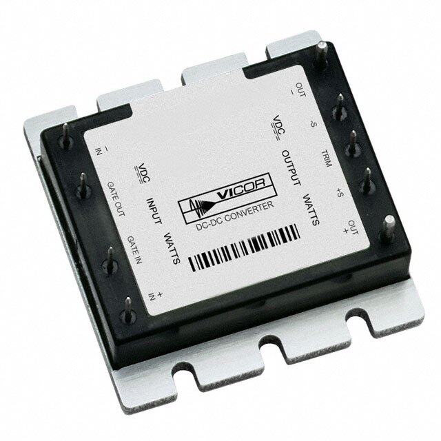
ICGOO电子元器件商城为您提供PTN78000AAS由Texas Instruments设计生产,在icgoo商城现货销售,并且可以通过原厂、代理商等渠道进行代购。 PTN78000AAS价格参考。Texas InstrumentsPTN78000AAS封装/规格:直流转换器, 非隔离 PoL 模块 DC/DC 转换器 1 输出 -15 ~ -3 V 1.5A 7V - 28.7V 输入。您可以下载PTN78000AAS参考资料、Datasheet数据手册功能说明书,资料中有PTN78000AAS 详细功能的应用电路图电压和使用方法及教程。
PTN78000AAS 是 Texas Instruments(德州仪器)生产的一款非隔离式直流-直流降压(Buck)转换器模块,广泛应用于需要高效、稳定电源转换的场合。

该模块的主要应用场景包括:

1. 工业控制系统:用于为PLC、工业自动化设备、传感器和执行器等提供稳定电源。

2. 通信设备:应用于基站、路由器、交换机等通信基础设施中,为内部电路提供高效的电源转换。

3. 测试与测量仪器:在示波器、信号发生器等精密仪器中,为各功能模块提供低噪声、高稳定性的电源。

4. 医疗设备:如便携式诊断设备、监护仪等对电源效率和稳定性有较高要求的场合。

5. 嵌入式系统与服务器:为嵌入式主板、服务器电源系统提供高效、紧凑的电源解决方案。

PTN78000AAS具备高转换效率、宽输入电压范围、过流与过温保护等特点,适合在对空间和效率有要求的中高功率应用中使用。
| 参数 | 数值 |
| 产品目录 | |
| 描述 | REGULATOR WIDE VIN 1.5A HORZ SMD非隔离式DC/DC转换器 1.5A Wide Inp/ Neg Out Adj Module |
| 产品分类 | DC DC ConvertersDC/DC转换器 |
| 品牌 | Texas Instruments |
| 产品手册 | |
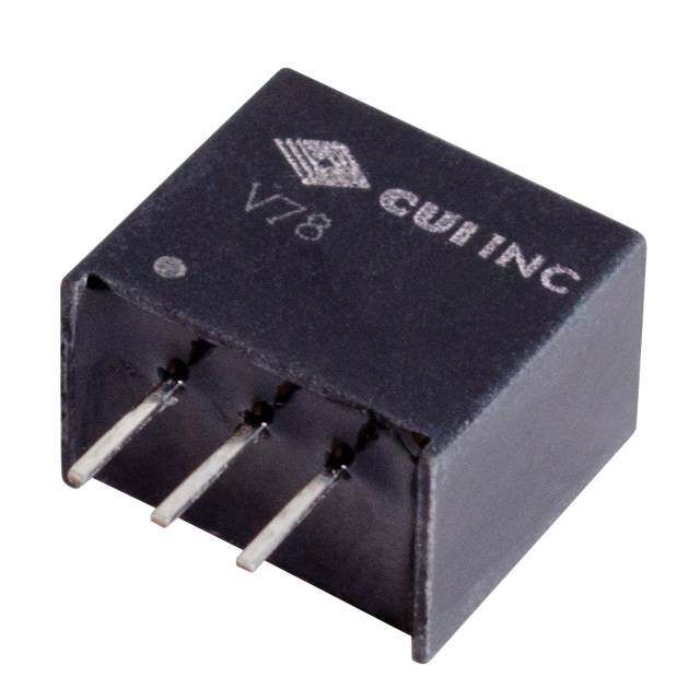
| 产品图片 |
|
| rohs | 否含铅 / 不符合限制有害物质指令(RoHS)规范要求 |
| 产品系列 | 非隔离式DC/DC转换器,Texas Instruments PTN78000AASPTN78000A |
| 数据手册 | |
| 产品型号 | PTN78000AAS |
| 产品 | Non-Isolated / POL |
| 产品种类 | 非隔离式DC/DC转换器 |
| 其它名称 | 296-19753 |
| 制造商产品页 | http://www.ti.com/general/docs/suppproductinfo.tsp?distId=10&orderablePartNumber=PTN78000AAS |
| 功率(W)-制造系列 | 9W |
| 功率(W)-最大值 | 9W |
| 包装 | 托盘 |
| 商标 | Texas Instruments |
| 大小/尺寸 | 0.75" 长 x 0.50" 宽 x 0.36" 高(19.1mm x 12.7mm x 9.1mm) |
| 安装类型 | 表面贴装 |
| 安装风格 | SMD/SMT |
| 封装 | Tray |
| 封装/外壳 | 5-SMD 模块 |
| 封装/箱体尺寸 | Surface Mount Module |
| 工作温度 | -40°C ~ 85°C |
| 工作温度范围 | - 40 C to + 85 C |
| 工厂包装数量 | 49 |
| 效率 | 84% |
| 标准包装 | 49 |
| 特性 | OTP, UVLO |
| 特色产品 | http://www.digikey.com/cn/zh/ph/texas-instruments/ptn78000.html |
| 电压-输入(最大值) | 28.7V |
| 电压-输入(最小值) | 7V |
| 电压-输出1 | -15 ~ -3 V |
| 电压-输出2 | - |
| 电压-输出3 | - |
| 电压-隔离 | - |
| 电流-输出(最大值) | 1.5A |
| 类型 | 非隔离 PoL 模块 |
| 系列 | PTN78000A |
| 输入电压范围 | 7 V to 29 V |
| 输出功率 | 9 W |
| 输出数 | 1 |
| 输出电压—通道1 | - 15 V to - 3 V |
| 输出电流—通道1 | 1.5 A |
| 输出端数量 | 1 |


- 商务部:美国ITC正式对集成电路等产品启动337调查
- 曝三星4nm工艺存在良率问题 高通将骁龙8 Gen1或转产台积电
- 太阳诱电将投资9.5亿元在常州建新厂生产MLCC 预计2023年完工
- 英特尔发布欧洲新工厂建设计划 深化IDM 2.0 战略
- 台积电先进制程称霸业界 有大客户加持明年业绩稳了
- 达到5530亿美元!SIA预计今年全球半导体销售额将创下新高
- 英特尔拟将自动驾驶子公司Mobileye上市 估值或超500亿美元
- 三星加码芯片和SET,合并消费电子和移动部门,撤换高东真等 CEO
- 三星电子宣布重大人事变动 还合并消费电子和移动部门
- 海关总署:前11个月进口集成电路产品价值2.52万亿元 增长14.8%


PDF Datasheet 数据手册内容提取
PTN78000A www.ti.com SLTS246B–APRIL2005–REVISEDJANUARY2006 1.5-A, WIDE-INPUT ADJUSTABLE BUCK-BOOST SWITCHING REGULATOR FEATURES APPLICATIONS • 1.5-AOutputCurrent • General-Purpose,IndustrialControls, HVACSystems,TestandMeasurement, • Wide-InputVoltage MedicalInstrumentation,AC/DCAdaptors, (7Vto29V) Vehicles,Marine,andAvionics • Wide-OutputVoltageAdjust (–15Vto–3V) • HighEfficiency(Upto84%) • OutputCurrentLimit • OvertemperatureShutdown • OperatingTemperature:–40°Cto85°C • Surface-MountPackageAvailable DESCRIPTION The PTN78000A is a series of high-efficiency, buck-boost integrated switching regulators (ISR), that represent the third generation in the evolution of the PT78NR100 series of products. In new designs, it should be considered in place of the PT78NR100 series of single in-line pin (SIP) products. The PTN78000A is smaller and lighter than its predecessor, and has either similar or improved electrical performance characteristics. The caseless, double-sided package also exhibits improved thermal characteristics, and is compatible with TI's roadmapforRoHSandlead-freecompliance. Operating from a wide-input voltage range, the PTN78000A provides high-efficiency, positive-to-negative voltage conversion for loads of up to 1.5 A. The output voltage is set using a single external resistor, and may be set to anyvaluewithintherange,–15Vto–3V. The PTN78000A has undervoltage lockout, and is suited to a wide variety of general-purpose applications that operateoff12-V,24-V,ortightlyregulated28-Vdcpower. GND 1 5 STANDARDAPPLICATION VI 2 P(TToNp78V0ie0w0A) + C3* 3 4 100(cid:2)F Electrolytic (Required) C1* C2* RSET# 100(cid:2)F 2x4.7(cid:2)F 1%,0.05W (Required) Electrolytic Ceramic (Required) (Required) VO GND *SeetheApplicationInformationforcapacitorrecommendation. #R isrequiredtoadjusttheoutputvoltagelowerthan-3V.SeetheApplicationInformationforvalues. SET Pleasebeawarethatanimportantnoticeconcerningavailability,standardwarranty,anduseincriticalapplicationsofTexas Instrumentssemiconductorproductsanddisclaimerstheretoappearsattheendofthisdatasheet. PRODUCTIONDATAinformationiscurrentasofpublicationdate. Copyright©2005–2006,TexasInstrumentsIncorporated Products conform to specifications per the terms of the Texas Instruments standard warranty. Production processing does not necessarilyincludetestingofallparameters.
PTN78000A www.ti.com SLTS246B–APRIL2005–REVISEDJANUARY2006 These devices have limited built-in ESD protection. The leads should be shorted together or the device placedinconductivefoamduringstorageorhandlingtopreventelectrostaticdamagetotheMOSgates. ORDERINGINFORMATION PTN78000A(BasicModel) Package OutputVoltage PartNumber Description Pb–freeandRoHSCompatible Designator PTN78000AAH HorizontalT/H Yes EUS –15Vto–3V PTN78000AAS(1)(2) HorizontalSMD No EUT PTN78000AAZ (1)(3) HorizontalSMD Yes EUT (1) AddaTsuffixfortapeandreeloptiononSMDpackages. (2) StandardoptionspecifiesSn/Pbsolderballmaterial. (3) Lead(Pb)-freeoptionspecifiesSn/Agsolderballmaterial. ABSOLUTE MAXIMUM RATINGS (1) overoperatingfree-airtemperaturerangeunlessotherwisenoted allvoltageswithrespecttoGND(pin1), PTN78000A UNIT T Operatingfree-airtemperature OverV range –40to85 A I Surfacetemperatureofmodulebody HorizontalSMD(suffix 260 Wavesoldertemperature orpins(5seconds) AH) HorizontalSMD(suffix 235 °C Surfacetemperatureofmodulebody AS) Solderreflowtemperature orpins HorizontalSMD(suffix 260 AZ) T Storagetemperature –40to125 stg (1) Stressesbeyondthoselistedunderabsolutemaximumratingsmaycausepermanentdamagetothedevice.Thesearestressratings only,andfunctionaloperationofthedeviceattheseoranyotherconditionsbeyondthoseindicatedunderrecommendedoperating conditionsisnotimplied.Exposuretoabsolute-maximum-ratedconditionsforextendedperiodsmayaffectdevicereliability. RECOMMENDED OPERATING CONDITIONS MIN MAX UNIT V Inputvoltage 7 32–|V | V I O T Operatingfree-airtemperature –40 85 °C A P Outputpower 9 W O PACKAGE SPECIFICATIONS PTN78000A(SuffixAH,AS,andAZ) Weight 2grams Flammability MeetsUL94V-O PerMil-STD-883D,Method2002.3,1ms,½sine, Mechanicalshock 500G (1) mounted HorizontalT/H(suffixAH) 20G (1) Mechanicalvibration Mil-STD-883D,Method2007.2,20-2000Hz HorizontalSMD(suffixAS&AZ) 15G (1) (1) Qualificationlimit. 2
PTN78000A www.ti.com SLTS246B–APRIL2005–REVISEDJANUARY2006 ELECTRICAL CHARACTERISTICS operatingat25°Cfree-airtemperature,V =12V,V =–5V,I =I (max),C =100μF,C =2x4.7μF,C =100μF(unless I O O O 1 2 3 otherwisenoted) PARAMETER TESTCONDITIONS MIN TYP MAX UNIT VO=–15V 0.1 0.6(1) VO=–12V 0.1 0.75(1) IO Outputcurrent TA=85°C,naturalconvectionairflow VO=–5V 0.1 1.5(1) A VO=–3.3V 0.1 1.5(1) VO=–15V 7 17(2) VO=–12V 7 20(2) VI Inputvoltagerange OverIOrange VO=–5V 7 27(2) V VO=–3.3V 7 28.7(2) Set-pointvoltagetolerance TA=25°C ±2%(3) Temperaturevariation –40°Cto85°C ±0.5% VO Lineregulation OverVIrange ±10 mV Loadregulation OverIOrange ±10 mV Totaloutputvoltage Includessetpoint,line,load ±3%(3) variation –40<TA<85°C VOAdj Orauntgpeutvoltageadjust 7V≤VI≤(32–|VO|)V –15 –3 V VI=12V,RSET=100Ω,VO=–15V 83% VI=12V,RSET=2kΩ,VO=–12V 84% η Efficiency VI=12V,RSET=28.7kΩ,VO=–5V 82% VI=12V,RSET=221kΩ,VO=–3.3V 77% Outputvoltageripple 20-MHzbandwidth 2%VO V(PP) IO(LIM) Currentlimitthreshold ΔVO=–50mV 3.2 A 1A/μsloadstepfrom50%to100%IOmax Transientresponse Recoverytime 200 μs VOover/undershoot 1 %VO FS Switchingfrequency OverVIandIOranges 440 550 660 kHz UVLO Undervoltagelockout VIincreasing 5.5 V Ceramic 9.4(4) μF CI Externalinputcapacitance Nonceramic 100(4) μF Ceramic 200 μF Externaloutput CO capacitance Nonceramic 100(5) 1,000 μF Equivalentseriesresistance(nonceramic) 14 (6) mΩ PerTelcordiaSR-332,50%stress, MTBF Calculatedreliability 8.9 106Hrs TA=40°C,groundbenign (1) Themaximumoutputcurrentis1.5Aorthemaximumoutputpoweris9W,whicheverisless. (2) Themaximuminputvoltageislimitedanddefinedtobe(32–|V |)volts. O (3) Theset-pointvoltagetoleranceisaffectedbythetoleranceandstabilityofR .ThestatedlimitisunconditionallymetifR hasa SET SET toleranceof1%with100ppm/°Corbettertemperaturestability. (4) A100-μFelectrolyticcapacitorandtwo4.7-μFceramiccapacitorsarerequiredacrosstheinput(V andGND)forproperoperation. I Locatetheceramiccapacitanceclosetothemodule. (5) 100μFofoutputcapacitanceisrequiredforproperoperation.Seetheapplicationinformationforfurtherguidance. (6) ThisisthetypicalESRforalltheelectrolytic(nonceramic)capacitance.Use17mΩastheminimumwhenusingmaximumESRvalues tocalculate. 3
PTN78000A www.ti.com SLTS246B–APRIL2005–REVISEDJANUARY2006 PIN ASSIGNMENT 1 5 PTN78000A (TopView) 2 3 4 TERMINALFUNCTIONS TERMINAL I/O DESCRIPTION NAME NO. ThenegativeoutputvoltagepowernodewithrespecttotheGNDnode.Itisalsothereferenceforthe V 1 O O V Adjustcontrolinputs. O V 2 I Thepositiveinputvoltagepowernodetothemodule,whichisreferencedtocommonGND. I N/C 3 Thispinisactiveandmustbeisolatedfromanyelectricalconnection. A1%resistormustbeconnectedbetweenpin1andpin4tosettheoutputvoltageofthemodulelower than–3V.Ifleftopen-circuit,theoutputvoltagedefaultsto–3V.Thetemperaturestabilityoftheresistor V Adjust 4 I O shouldbe100ppm/°C(orbetter).Theset-pointrangeis–15Vto–3V.Thestandardresistorvaluefor anumberofcommonoutputvoltagesisprovidedintheapplicationinformation. GND 5 I/O ThecommongroundconnectionfortheV andV powerconnections. I O 4
PTN78000A www.ti.com SLTS246B–APRIL2005–REVISEDJANUARY2006 TYPICAL CHARACTERISTICS (7-V INPUT)(1)(2) EFFICIENCY OUTPUTVOLTAGERIPPLE POWERDISSIPATION vs vs vs OUTPUTCURRENT OUTPUTCURRENT OUTPUTCURRENT 90 P 140 2.5 85 mVP 120 VO=-12V W VO=-12V 80 - - 2 VO=-15V Efficiency-% 567567555000 VO=-15VVO=VO-12=V-V5OV=-3V -OutputVoltageRipple 10246800000 VO=-15V VO=-3V VO=-5V P-PowerDissipationD 01..551 VO=-3VVO=-5V 450 0.3 0.6 0.9 1.2 1.5 VO 00 0.3 0.6 0.9 1.2 1.5 00 0.3 0.6 0.9 1.2 1.5 IO-OutputCurrent-A IO-OutputCurrent-A IO-OutputCurrent-A Figure1. Figure2. Figure3. TEMPERATUREDERATING TEMPERATUREDERATING TEMPERATUREDERATING vs vs vs OUTPUTCURRENT OUTPUTCURRENT OUTPUTCURRENT 90 90 90 ombientTemperature-C 5467800000 200LFM 100NLaFtMconv ombientTemperature-C 5467800000 200LF1M00NLaFtMconv ombientTemperature-C 5467800000 200LFM100NaLtFcMonv A VO=-5V A VO=-12V A VO=-15V 30 30 30 20 20 20 0 0.5 1 1.5 0 0.25 0.5 0.75 0 0.1 0.2 0.3 0.4 0.5 0.6 IO-OutputCurrent-A IO-OutputCurrent-A IO-OutputCurrent-A Figure4. Figure5. Figure6. (1) Theelectricalcharacteristicdatahasbeendevelopedfromactualproductstestedat25°C.Thisdataisconsideredtypicalforthe converter.AppliestoFigure1,Figure2,andFigure3. (2) Thetemperaturederatingcurvesrepresenttheconditionsatwhichinternalcomponentsareatorbelowthemanufacturer'smaximum operatingtemperatures.Deratinglimitsapplytomodulessoldereddirectlytoa100mmx100mm,double-sidedPCBwith2oz.copper. Forsurfacemountpackages,multiplevias(platedthroughholes)arerequiredtoaddthermalpathstothepowerpins.Pleasereferto themechanicalspecificationformoreinformation.AppliestoFigure4,Figure5,andFigure6. 5
PTN78000A www.ti.com SLTS246B–APRIL2005–REVISEDJANUARY2006 TYPICAL CHARACTERISTICS (12-V INPUT)(1)(2) EFFICIENCY OUTPUTVOLTAGERIPPLE POWERDISSIPATION vs vs vs OUTPUTCURRENT OUTPUTCURRENT OUTPUTCURRENT 90 P100 2 85 mVP 90 VO=-15V W 1.8 VO=-15V VO=-12V Efficiency-% 56756785550000 VO=-1V5OV=-12VVO=V-5OV=-3V -OutputVoltageRipple- 1234756800000000 VO=-3VOV=-V1O2V=-5V P-PowerDissipation-D0101001.......44668221 VO=-3VVO=-5V 45 O 0 0 0 0.5 1 1.5 V 0 0.5 1 1.5 0 0.5 1 1.5 IO-OutputCurrent-A IO-OutputCurrent-A IO-OutputCurrent-A Figure7. Figure8. Figure9. TEMPERATUREDERATING TEMPERATUREDERATING TEMPERATUREDERATING vs vs vs OUTPUTCURRENT OUTPUTCURRENT OUTPUTCURRENT 90 90 90 oC 80 oC 80 oC 80 ure- 70 200LFM ure- 70 200LFM ure- 70 200LFM perat 60 100LFM perat 60 100LFM perat 60 100LFM ntTem 50 Natconv ntTem 50 Natconv ntTem 50 Natconv mbie 40 mbie 40 mbie 40 A VO=-5Vand-3V A VO=-12V A VO=-15V 30 30 30 20 20 20 0 0.5 1 1.5 0 0.25 0.5 0.75 0 0.1 0.2 0.3 0.4 0.5 0.6 IO-OutputCurrent-A IO-OutputCurrent-A IO-OutputCurrent-A Figure10. Figure11. Figure12. (1) Theelectricalcharacteristicdatahasbeendevelopedfromactualproductstestedat25°C.Thisdataisconsideredtypicalforthe converter.AppliestoFigure7,Figure8,andFigure9. (2) Thetemperaturederatingcurvesrepresenttheconditionsatwhichinternalcomponentsareatorbelowthemanufacturer'smaximum operatingtemperatures.Deratinglimitsapplytomodulessoldereddirectlytoa100-mmx100-mm,double-sidedPCBwith2oz.copper. Forsurfacemountpackages,multiplevias(platedthroughholes)arerequiredtoaddthermalpathstothepowerpins.Pleasereferto themechanicalspecificationformoreinformation.AppliestoFigure10,Figure11,andFigure12. 6
PTN78000A www.ti.com SLTS246B–APRIL2005–REVISEDJANUARY2006 TYPICAL CHARACTERISTICS (24-V INPUT)(1)(2) EFFICIENCY OUTPUTVOLTAGERIPPLE POWERDISSIPATION vs vs vs OUTPUTCURRENT OUTPUTCURRENT OUTPUTCURRENT 85 70 2 P 80 mVP 60 1.8 Efficiency-% 567567555000 VO=-5V VO=-3V -OutputVoltageRipple-O 1234500000 VO=-5V VO=-3V P-PowerDissipation-WD 0101001.......44668221 VO=-5VVO=-3V V 45 0 0 0 0.3 0.6 0.9 1.2 1.5 0 0.3 0.6 0.9 1.2 1.5 0 0.3 0.6 0.9 1.2 1.5 IO-OutputCurrent-A IO-OutputCurrent-A IO-OutputCurrent-A Figure13. Figure14. Figure15. TEMPERATUREDERATING vs OUTPUTCURRENT 90 oC 80 - e ur 70 200LFM at per 60 100LFM m Te 50 Natconv nt e mbi 40 A VO=-5Vand-3V 30 20 0 0.5 1 1.5 IO-OutputCurrent-A Figure16. (1) Theelectricalcharacteristicdatahasbeendevelopedfromactualproductstestedat25°C.Thisdataisconsideredtypicalforthe converter.AppliestoFigure13,Figure14,andFigure15. (2) Thetemperaturederatingcurvesrepresenttheconditionsatwhichinternalcomponentsareatorbelowthemanufacturer'smaximum operatingtemperatures.Deratinglimitsapplytomodulessoldereddirectlytoa100-mmx100-mm,double-sidedPCBwith2oz.copper. Forsurfacemountpackages,multiplevias(platedthroughholes)arerequiredtoaddthermalpathstothepowerpins.Pleasereferto themechanicalspecificationformoreinformation.AppliestoFigure16. 7
PTN78000A www.ti.com SLTS246B–APRIL2005–REVISEDJANUARY2006 APPLICATION INFORMATION Adjusting the Output Voltage of the PTN78000A Wide-Output Adjust Power Modules General A resistor must be connected directly between the V Adjust control (pin 4) and the output voltage (pin 7) to set O the output voltage lower than –3 V. The adjustment range is from –15 V to –3 V. If pin 4 is left open, the output voltagedefaultstothehighestvalue,–3V. Table 1 gives the standard resistor value for a number of common voltages, and with the actual output voltage that the value produces. For other output voltages, the resistor value can either be calculated using the following formula, or simply selected from the range of values given in Table 2. Figure 17 shows the placement of the requiredresistor. 1.25V R =54.9k(cid:3) (cid:4) -5.62k(cid:3) SET |V |-3V O InputVoltageConsiderations The PTN78000A is a buck-boost switching regulator. In order that the output remains in regulation, the input voltagemustnotexceedtheoutputbyamaximumdifferentialvoltage. Forsatisfactoryperformance,themaximumoperatinginputvoltageis(32-|V |)volts. O As an example, Table 1 gives the operating input voltage range for the common output bus voltages. In addition, theElectricalCharacteristicsdefinetheavailableoutputvoltageadjustrangeforvariousinputvoltages. Table1.StandardValuesofR forCommonOutput set Voltages VO RSET VO Operating (Required) (StandardValue) (Actual) VIRange –15V 100Ω –14.997V 9Vto17V –12V 2kΩ –12.006V 9Vto20V –5V 28.7kΩ –5.000V 9Vto27V –3.3V 221kΩ –3.303V 9Vto28.7V PTN78000A VI 2 5 GND VI GND Adj VO + C3 + 4 1 C1 C2 RSET 0.05W V 1% O GND (1) A 0.05-W rated resistor may be used. The tolerance should be 1%, with a temperature stability of 100 ppm/°C (or better). Place the resistor as close to the regulator as possible. Connect the resistor directly between pins 4 and 1 usingdedicatedPCBtraces. (2) NeverconnectcapacitorsfromV AdjusttoeitherGNDorV .AnycapacitanceaddedtotheV Adjustpinaffectsthe O O O stabilityoftheregulator. Figure17.V AdjustResistorPlacement O 8
PTN78000A www.ti.com SLTS246B–APRIL2005–REVISEDJANUARY2006 Table2.OutputVoltageSet-PointResistorValues VORequired RSET VORequired RSET VORequired RSET –15.0V 99Ω –11.9V 2.09kΩ –8.8V 6.21kΩ –14.9V 147Ω –11.8V 2.18kΩ –8.6V 6.63kΩ –14.8V 196Ω –11.7V 2.27kΩ –8.4V 7.09kΩ –14.7V 245Ω –11.6V 2.36kΩ –8.2V 7.58kΩ –14.6V 296Ω –11.5V 2.45kΩ –8.0V 8.11kΩ –14.5V 347Ω –11.4V 2.55kΩ –7.8V 8.68kΩ –14.4V 400Ω –11.3V 2.65kΩ –7.6V 9.30kΩ –14.3V 453Ω –11.2V 2.75kΩ –7.4V 9.98kΩ –14.2V 507Ω –11.1V 2.82kΩ –7.2V 10.7kΩ –14.1V 562Ω –11.0V 2.96kΩ –7.0V 11.5kΩ –14.0V 619Ω –10.9V 3.07kΩ –6.8V 12.4kΩ –13.9V 676Ω –10.8V 3.18kΩ –6.6V 13.4kΩ –13.8V 734Ω –10.7V 3.29kΩ –6.4V 14.6kΩ –13.7V 794Ω –10.6V 3.41kΩ –6.2V 15.8kΩ –13.6V 854Ω –10.5V 3.53kΩ –6.0V 17.3kΩ –13.5V 916Ω –10.4V 3.65kΩ –5.8V 18.9kΩ –13.4V 979Ω –10.3V 3.78kΩ –5.6V 20.7kΩ –13.3V 1.04kΩ –10.2V 3.91kΩ –5.4V 22.9kΩ –13.2V 1.11kΩ –10.1V 4.04kΩ –5.2V 25.6kΩ –13.1V 1.18kΩ –10.0V 4.18kΩ –5.0V 28.7kΩ –13.0V 1.24kΩ –9.9V 4.33kΩ –4.8V 32.5kΩ –12.9V 1.31kΩ –9.8V 4.47kΩ –4.6V 37.2kΩ –12.8V 1.38kΩ –9.7V 4.62kΩ –4.4V 43.4kΩ –12.7V 1.46kΩ –9.6V 4.78kΩ –4.2V 51.6kΩ –12.6V 1.52kΩ –9.5V 4.94kΩ –4.0V 63.0kΩ –12.5V 1.60kΩ –9.4V 5.10kΩ –3.8V 80.1kΩ –12.4V 1.68kΩ –9.3V 5.27kΩ –3.6V 109kΩ –12.3V 1.76kΩ –9.2V 5.45kΩ –3.4V 166kΩ –12.2V 1.84kΩ –9.1V 5.63kΩ –3.2V 338kΩ –12.1V 1.92kΩ –9.0V 5.82kΩ –3.0V OPEN –12.0V 2.01kΩ –8.9V 6.01kΩ 9
PTN78000A www.ti.com SLTS246B–APRIL2005–REVISEDJANUARY2006 CAPACITOR RECOMMENDATIONS FOR THE PTN78000 WIDE-OUTPUT ADJUST POWER MODULES InputCapacitor The minimum requirements for the input bus is 100 μF of nonceramic capacitance and 9.4 μF (2 x 4.7 μF) of ceramic capacitance, in either an X5R or X7R temperature characteristic, and 100 μF of electrolytic capacitance. Ceramic capacitors should be located within 0.5 inch (1,27 cm) of the regulator's input pins. Electrolytic capacitors should be used at the input in addition to the required ceramic capacitance. The minimum ripple current rating for any nonceramic capacitance must be at least 250 mA rms. The ripple current rating of electrolytic capacitors is a major consideration when they are used at the input. This ripple current requirement canbereducedbyplacingmoreceramiccapacitorsattheinput,inadditiontotheminimumrequired9.4 μF. Tantalum capacitors are not recommended for use at the input bus, as none were found to meet the minimum voltage rating of 2 × (maximum dc voltage + ac ripple). The 2× rating is standard practice for regular tantalum capacitors to ensure reliability. Polymer-tantalum capacitors are more reliable and are available with a maximum ratingoftypically20V.Thesecanbeusedwithinputvoltagesupto16V. OutputCapacitor The minimum capacitance required to ensure stability is a 100 μF. Either ceramic or electrolytic-type capacitors can be used. The minimum ripple current rating for the nonceramic capacitance must be at least 200 mA rms. The stability of the module and voltage tolerances is compromised if the capacitor is not placed near the output bus pins. A high-quality, computer-grade electrolytic capacitor should be adequate. A ceramic capacitor can be alsobelocatedwithin0.5inch(1,27cm)oftheoutputpin. For applications with load transients (sudden changes in load current), the regulator response improves with additional capacitance. Additional electrolytic capacitors should be located close to the load circuit. These capacitors provide decoupling over the frequency range, 2 kHz to 150 kHz. Aluminum electrolytic capacitors are suitable for ambient temperatures above 0°C. For operation below 0°C, tantalum or Os-Con-type capacitors are recommended. When using one or more nonceramic capacitors, the calculated equivalent ESR should be no lowerthan14mΩ(17mΩusingthemanufacturer'smaximumESRforasinglecapacitor).A list of recommended capacitorsandvendorsareidentifiedin Table3. CeramicCapacitors Above 150 kHz, the performance of aluminum electrolytic capacitors becomes less effective. To further reduce the reflected input ripple current, or the output transient response, multilayer ceramic capacitors must be added. Ceramic capacitors have low ESR, and their resonant frequency is higher than the bandwidth of the regulator. When placed at the output, their combined ESR is not critical as long as the total value of ceramic capacitance doesnotexceed200 μF. TantalumCapacitors Tantalum-type capacitors may be used at the output, and are recommended for applications where the ambient operating temperature can be less than 0°C. The AVX TPS, Sprague 593D/594/595, and Kemet T495/T510/T520capacitorsseriesaresuggestedover many other tantalum types due to their rated surge, power dissipation, and ripple current capability. As a caution, many general-purpose tantalum capacitors have considerably higher ESR, reduced power dissipation, and lower ripple current capability. These capacitors are alsolessreliableastheyhavelowerpowerdissipationandsurgecurrent ratings. Tantalum capacitors that do not have a stated ESR or surge current rating are not recommended for power applications. When specifying Os-Con and polymer-tantalum capacitors for the output, the minimum ESR limit is encountered well before the maximumcapacitancevalueisreached. CapacitorTable The capacitor table, Table 3, identifies the characteristics of capacitors from various vendors with acceptable ESR and ripple current (rms) ratings. The recommended number of capacitors required at both the input and output buses is identified for each capacitor type. This is not an extensive capacitor list. Capacitors from other vendors are available with comparable specifications. Those listed are for guidance. The rms rating and ESR (at 100 kHz) are critical parameters necessary to ensure both optimum regulator performance and long capacitor life. 10
PTN78000A www.ti.com SLTS246B–APRIL2005–REVISEDJANUARY2006 DesigningforLoadTransients The transient response of the dc/dc converter has been characterized using a load transient with a di/dt of 1 A/μs.The typical voltage deviation for this load transient is given in the data sheet specification table using the required value of output capacitance. As the di/dt of a transient is increased, the response of a converter's regulation circuit ultimately depends on its output capacitor decoupling network. This is an inherent limitation of any dc/dc converter once the speed of the transient exceeds its bandwidth capability. If the target application specifies a higher di/dt or lower voltage deviation, the requirement can only be met with additional output capacitor decoupling. In these cases, special attention must be paid to the type, value, and ESR of the capacitorsselected. If the transient performance requirements exceed those specified in the data sheet, the selection of output capacitors becomes more important. Review the minimum ESR in the characteristic data sheet for details on the capacitancemaximum. Table3.RecommendedInput/OutputCapacitors CAPACITORCHARACTERISTICS QUANTITY CAPACCOISMTEOPRORIENVSEENNTDOR/ WVOOLRTKAINGGE VA(μLFU)E REQESSUEIISVRTAIAELNSECNET MRA8IXP5IP°MCLUEM PHYSSIZIECAL INBPUUST OUBTUPSUT NVUENMDBOERR (V) CURRENT (mm) (ESR)(Ω) (Irms)(mA) FC(Radial) 35 100 0.117 550 8×11,5 ≥1 1 EEUFC1H181 FC(SMD) 35 100 0.015 670 10×10,2 ≥1(1) 1 EEVFC1V101P UnitedChemi-ConPXA(SMD) 16 180 0.016 4360 8×12 ≥1(1) ≤1 PXA16VC180MF60(VI,|VO|< 14V) PS 25 100 0.020 4300 8×10,5 ≥1(1) ≤1 10FS100M(VI,|VO|<22V) LXZ 50 100 0.220 485 8×12,5 ≥1 1 LXZ50VB101M8X12LL MVY50VC101M10X10TP MVY(SMD) 50 100 0.300 500 10×10 ≥1 1 (|VO|≤5V) NichiconUWG(SMD) 50 100 0.300 500 10×10 ≥1 1 UWG1H101MNR1GS F550(Tantalum) 10 100 0.055 2000 7.7×4,3 N/R(1) ≤3(2) F551A107MN(|VO|≤5V) HD 50 120 0.072 979 10×12,5 ≥1 1 UHD1H101MPR SanyoOs-ConSVP(SMD) 20 100 0.024 2500 8×12 ≥1(1) ≤1 20SVP100M(VI,|VO|≤16V) SP 16 100 0.032 2890 10×5 ≥1(1) ≤1 16SP100M(VI,|VO|≤14V) 7,3L×4,3 TPSV107M020R0085 20 100 0.085 1543 N/R(3) ≤2 W×4,1H (|VO|≤10V) AVXTantalumTPS(SMD) TPSE107M020R0200 20 100 0.200 >817 N/R(3) ≤2 (|VO|≤10V) GRM32ER61C476M MurataX5RCeramic 16 47 0.002 >1000 3225 1(1) ≤2 (|Vo|~VI≤13.5V) GRM422X5R476M6.3 MurataX5RCeramic 6.3 47 0.002 >1000 3225 N/R(1) ≤2 (|VO|≤5.5V) C3225X7R1E225KT/MT TDKX7RCeramic 25 2.2 0.002 >1000 SMD ≥4(4) 1 (|VO|≤20V) GRM32RR71E225K MurataX7RCeramic 25 2.2 0.002 >1000 3225 ≥4(4) 1 (|VO|≤20V) C1210C225K3RAC KemetX7RCeramic 25 2.2 0.002 >1000 3225 ≥4(4) 1 (|VO|≤20V) 12103C225KAT2A AVXX7RCeramic 25 2.2 0.002 >1000 3225 ≥4(4) 1 (|VO|≤20V) MurataX7RCeramic 50 4.7 0.002 >1000 3225 ≥2 1 GRM32ER71H475KA88L TDKX7RCeramic 50 2.2 0.002 >1000 ≥4 1 C3225X7R1H225KT MurataRadialThrough-hole 50 2.2 0.004 >1000 ≥4 1 RPER71H2R2KK6F03 (1) Thevoltageratingoftheinputcapacitormustbeselectedforthedesiredoperatinginputvoltagerangeoftheregulator.Tooperatethe regulatoratahigherinputvoltage,selectacapacitorwiththenexthighervoltagerating. (2) Themaximumvoltageratingofthecapacitormustbeselectedforthedesiredset-pointvoltage(V ).Tooperateatahigheroutput O voltage,selectacapacitorwithahighervoltagerating. (3) Notrecommended(N/R).Thevoltageratingdoesnotmeettheminimumoperatinglimitsinmostapplications. (4) Themaximumratingoftheceramiccapacitorlimitstheregulator'soperatinginputvoltageto20V.Selectaalternativeceramic componenttooperateatahigherinputvoltage. 11
PTN78000A www.ti.com SLTS246B–APRIL2005–REVISEDJANUARY2006 Power-Up Characteristics When configured per the standard application, the PTN78000A power module produces a regulated output voltagefollowingtheapplicationofavalidinputsourcevoltage.Duringpowerup,internalsoft-start circuitry slows the rate that the output voltage rises, thereby limiting the amount of in-rush current that can be drawn from the input source. The soft-start circuitry introduces a short time delay (typically 5 ms – 10 ms) into the power-up characteristic. This is from the point that a valid input source is recognized. Figure 18 shows the power-up waveforms for a PTN78000A, operating from a 12-V input and with the output voltage adjusted to –5 V. The waveformsweremeasuredwitha1.5-Aresistiveload. VI(5V/div) VO(2V/div) I (1A/div) I t-Time=5ms/div Figure18.Power-UpWaveforms Undervoltage Lockout The undervoltage lockout (UVLO) circuit prevents the module from attempting to power up until the input voltage is above the UVLO threshold. This prevents the module from drawing excessive current from the input source at powerup.BelowtheUVLOthreshold,themoduleisheldoff. Current Limit Protection The PTN78000 modules protect against load faults with a continuous current limit characteristic. Under a load fault condition, the output current cannot exceed the current limit value. Attempting to draw current that exceeds the current limit value causes the module to progressively reduce its output voltage. Current is continuously supplied to the fault until it is removed. On removal of the fault, the output voltage promptly recovers. When limiting output current, the regulator experiences higher power dissipation, which increases its temperature. If the temperature increase is excessive, the module's overtemperature protection begins to periodically turn the output voltagecompletelyoff. Overtemperature Protection A thermal shutdown mechanism protects the module's internal circuitry against excessively high temperatures. A riseintemperaturemaybetheresultof a drop in airflow, a high ambient temperature, or a sustained current-limit condition. If the junction temperature of the internal control IC rises excessively, the module turns itself off, reducing the output voltage to zero. The module instantly restarts when the sensed temperature decreases by a fewdegrees. Note: Overtemperature protection is a last-resort mechanism to prevent damage to the module. It should not be relied on as permanent protection against thermal stress. Always operate the module within its temperature derated limits, for the worst-case operating conditions of output current, ambient temperature, and airflow. Operating the module above these limits, albeit below the thermal shutdown temperature, reduces the long-term reliabilityofthemodule. 12
PTN78000A www.ti.com SLTS246B–APRIL2005–REVISEDJANUARY2006 Optional Input/Output Filters Power modules include internal input and output ceramic capacitors in all their designs. However, some applications require much lower levels of either input reflected or output ripple/noise. This application describes variousfiltersanddesigntechniquesfoundtobesuccessfulinreducingbothinputandoutputripple/noise. Input/OutputCapacitors The easiest way to reduce output ripple and noise is to add one or more 1-μF ceramic capacitors, such as C5 shown in Figure 19. Ceramic capacitors should be placed close to the output power terminals. A single 4.7-μF capacitorreducestheoutputripple/noiseby10%to30%formodules with a rated output current of less than 3 A. (Note: C4 is recommended to improve the regulators transient response and does not reduce output ripple and noise.) Switching regulators draw current from the input line in pulses at their operating frequency. The amount of reflected (input) ripple/noise generated is directly proportional to the equivalent source impedance of the power source including the impedance of any input lines. The addition of C1, minimum 4.7-μF ceramic capacitor, near theinputpowerpins,reducesreflectedconductedripple/noiseby20%to30%. VI 2 PTN78000A 1 VO V V I O GND Adj 5 4 C1 C2 C3 C4 C5 R 4.7(cid:2)F 100(cid:2)F 2x4.7(cid:2)F SET 100(cid:2)F 4.7(cid:2)F Ceramic Electrolytic Ceramic (Required) Ceramic (Required) (Required) (SeeNoteB) (SeeNoteA) GND GND A. Seespecificationsforrequiredvalueandtype. B. SeeApplicationInformationforsuggestedvalueandtype. Figure19.AddingHigh-FrequencyBypassCapacitorstotheInputandOutput πFilters If a further reduction in ripple/noise level is required for an application, higher order filters must be used. A π (pi) filter, employing a ferrite bead (Fair-Rite Pt. No. 2673000701 or equivalent) in series with the input or output terminals of the regulator reduces the ripple/noise by at least 20 db (see Figure 20 and Figure 21). In order for the inductor to be effective in reduction of ripple and noise ceramic capacitors are required. (See the Capacitor RecommendationsforthePTN78000Aforadditionalinformationonvendorsandcomponentsuggestions.) These inductors plus ceramic capacitors form an excellent filter because of the rejection at the switching frequency (650 kHz - 1 MHz). The placement of this filter is critical. It must be located as close as possible to the input or output pins to be effective. The ferrite bead is small (12,5 mm × 3 mm), easy to use, low cost, and has low dc resistance. Fair-Rite also manufactures a surface-mount bead (part number 2773021447), through hole (part number 2673000701) rated to 5 A. Alternatively, 1-μH to 5-μH inductors can be used in place of the ferrite inductorbead. 13
PTN78000A www.ti.com SLTS246B–APRIL2005–REVISEDJANUARY2006 L1 L2 V 1-5(cid:2)H 1-5(cid:2)H V I 2 VI PTN78000A VO 1 O GND Adj 5 4 C1 C2 C3 C4 C5 4C.e7ra(cid:2)mFic 1E0le0c(cid:2)trFolytic 2Cexra4m.7i(cid:2)cF RSET 1(R0e0q(cid:2)uFired) 4.7(cid:2)F C(S6eeNoteC) Ceramic (Required) (Required) (SeeNoteB) (SeeNoteA) GND GND A. Seespecificationsforrequiredvalueandtype. B. SeeApplicationInformationforsuggestedvalueandtype. C. Recommendedforapplicationswithloadtransients. Figure20.AddingπFilters(I ≤3A) O 45 40 35 B d n − 30 1 MHz o ati u n 25 e Att 20 600 kHz 15 10 0 0.5 1 1.5 2 2.5 3 Load Current − A Figure21.π-FilterAttenuationvs.LoadCurrent 14
PACKAGE OPTION ADDENDUM www.ti.com 19-Dec-2019 PACKAGING INFORMATION Orderable Device Status Package Type Package Pins Package Eco Plan Lead/Ball Finish MSL Peak Temp Op Temp (°C) Device Marking Samples (1) Drawing Qty (2) (6) (3) (4/5) PTN78000AAH ACTIVE Through- EUS 5 56 RoHS (In SN N / A for Pkg Type -40 to 85 Hole Module Work) & Green (In Work) PTN78000AAS ACTIVE Surface EUT 5 49 Non-RoHS SNPB Level-1-235C-UNLIM/ -40 to 85 Mount Module & Green Level-3-260C-168HRS (In Work) PTN78000AAST ACTIVE Surface EUT 5 250 Non-RoHS SNPB Level-1-235C-UNLIM/ -40 to 85 Mount Module & Green Level-3-260C-168HRS (In Work) PTN78000AAZ ACTIVE Surface EUT 5 49 RoHS (In SNAGCU Level-3-260C-168 HR -40 to 85 Mount Module Work) & Green (In Work) PTN78000AAZT ACTIVE Surface EUT 5 250 RoHS (In SNAGCU Level-3-260C-168 HR -40 to 85 Mount Module Work) & Green (In Work) (1) The marketing status values are defined as follows: ACTIVE: Product device recommended for new designs. LIFEBUY: TI has announced that the device will be discontinued, and a lifetime-buy period is in effect. NRND: Not recommended for new designs. Device is in production to support existing customers, but TI does not recommend using this part in a new design. PREVIEW: Device has been announced but is not in production. Samples may or may not be available. OBSOLETE: TI has discontinued the production of the device. (2) RoHS: TI defines "RoHS" to mean semiconductor products that are compliant with the current EU RoHS requirements for all 10 RoHS substances, including the requirement that RoHS substance do not exceed 0.1% by weight in homogeneous materials. Where designed to be soldered at high temperatures, "RoHS" products are suitable for use in specified lead-free processes. TI may reference these types of products as "Pb-Free". RoHS Exempt: TI defines "RoHS Exempt" to mean products that contain lead but are compliant with EU RoHS pursuant to a specific EU RoHS exemption. Green: TI defines "Green" to mean the content of Chlorine (Cl) and Bromine (Br) based flame retardants meet JS709B low halogen requirements of <=1000ppm threshold. Antimony trioxide based flame retardants must also meet the <=1000ppm threshold requirement. (3) MSL, Peak Temp. - The Moisture Sensitivity Level rating according to the JEDEC industry standard classifications, and peak solder temperature. (4) There may be additional marking, which relates to the logo, the lot trace code information, or the environmental category on the device. (5) Multiple Device Markings will be inside parentheses. Only one Device Marking contained in parentheses and separated by a "~" will appear on a device. If a line is indented then it is a continuation of the previous line and the two combined represent the entire Device Marking for that device. Addendum-Page 1
PACKAGE OPTION ADDENDUM www.ti.com 19-Dec-2019 (6) Lead/Ball Finish - Orderable Devices may have multiple material finish options. Finish options are separated by a vertical ruled line. Lead/Ball Finish values may wrap to two lines if the finish value exceeds the maximum column width. Important Information and Disclaimer:The information provided on this page represents TI's knowledge and belief as of the date that it is provided. TI bases its knowledge and belief on information provided by third parties, and makes no representation or warranty as to the accuracy of such information. Efforts are underway to better integrate information from third parties. TI has taken and continues to take reasonable steps to provide representative and accurate information but may not have conducted destructive testing or chemical analysis on incoming materials and chemicals. TI and TI suppliers consider certain information to be proprietary, and thus CAS numbers and other limited information may not be available for release. In no event shall TI's liability arising out of such information exceed the total purchase price of the TI part(s) at issue in this document sold by TI to Customer on an annual basis. Addendum-Page 2
None
None
IMPORTANTNOTICEANDDISCLAIMER TIPROVIDESTECHNICALANDRELIABILITYDATA(INCLUDINGDATASHEETS),DESIGNRESOURCES(INCLUDINGREFERENCE DESIGNS),APPLICATIONOROTHERDESIGNADVICE,WEBTOOLS,SAFETYINFORMATION,ANDOTHERRESOURCES“ASIS” ANDWITHALLFAULTS,ANDDISCLAIMSALLWARRANTIES,EXPRESSANDIMPLIED,INCLUDINGWITHOUTLIMITATIONANY IMPLIEDWARRANTIESOFMERCHANTABILITY,FITNESSFORAPARTICULARPURPOSEORNON-INFRINGEMENTOFTHIRD PARTYINTELLECTUALPROPERTYRIGHTS. TheseresourcesareintendedforskilleddevelopersdesigningwithTIproducts.Youaresolelyresponsiblefor(1)selectingtheappropriate TIproductsforyourapplication,(2)designing,validatingandtestingyourapplication,and(3)ensuringyourapplicationmeetsapplicable standards,andanyothersafety,security,orotherrequirements.Theseresourcesaresubjecttochangewithoutnotice.TIgrantsyou permissiontousetheseresourcesonlyfordevelopmentofanapplicationthatusestheTIproductsdescribedintheresource.Other reproductionanddisplayoftheseresourcesisprohibited.NolicenseisgrantedtoanyotherTIintellectualpropertyrightortoanythird partyintellectualpropertyright.TIdisclaimsresponsibilityfor,andyouwillfullyindemnifyTIanditsrepresentativesagainst,anyclaims, damages,costs,losses,andliabilitiesarisingoutofyouruseoftheseresources. TI’sproductsareprovidedsubjecttoTI’sTermsofSale(www.ti.com/legal/termsofsale.html)orotherapplicabletermsavailableeitheron ti.comorprovidedinconjunctionwithsuchTIproducts.TI’sprovisionoftheseresourcesdoesnotexpandorotherwisealterTI’sapplicable warrantiesorwarrantydisclaimersforTIproducts. MailingAddress:TexasInstruments,PostOfficeBox655303,Dallas,Texas75265 Copyright©2019,TexasInstrumentsIncorporated